

LT1939
Monolithic 2A Step-Down
Regulator Plus Linear
Regulator/Controller
FEATURES
n
Wide Input Range: 3V to 25V
n
Short-Circuit Protected Over Full Input Range
n
2A Output Current Capability
n
Adjustable/Synchronizable Fixed Frequency
Operation from 250kHz to 2.2MHz
n
Soft-Start/Tracking Capability
n
Output Adjustable Down to 0.8V
n
Adjustable Linear Regulator/Driver with 13mA
Output Capability
n
Power Good Comparator with Complementary
Outputs
n
Low Shutdown Current: 12µA
n
Thermally Enhanced 3mm × 3mm DFN Package
APPLICATIONS
n
Automotive Battery Regulation
n
Industrial Control
n
Wall Transformer Regulation
n
Distributed Power Regulation
DESCRIPTION
The LT®1939 is a current mode PWM step-down DC/DC
converter with an internal 2.3A switch. The wide input
range of 3V to 25V makes the LT1939 suitable for regulating power from a wide variety of sources, including
automotive batteries, industrial supplies and unregulated
wall adapters.
Resistor-programmable 250kHz to 2.2MHz frequency
range and synchronization capability enable optimization
between effi ciency and external component size. Cycleby-cycle current limit, frequency foldback and thermal
shutdown provide protection against a shorted output.
The soft-start feature controls the ramp rate of the output
voltage, eliminating input current surge during start-up,
and also provides output tracking.
The LT1939 contains an internal NPN transistor with feedback control which can be confi gured as a linear regulator
or as a linear regulator controller.
The LT1939’s low current shutdown mode (<12µA) enables
easy power management in battery-powered systems.
L, LT, LTC and LTM are registered trademarks of Linear Technology Corporation.
All other trademarks are the property of their respective owners.
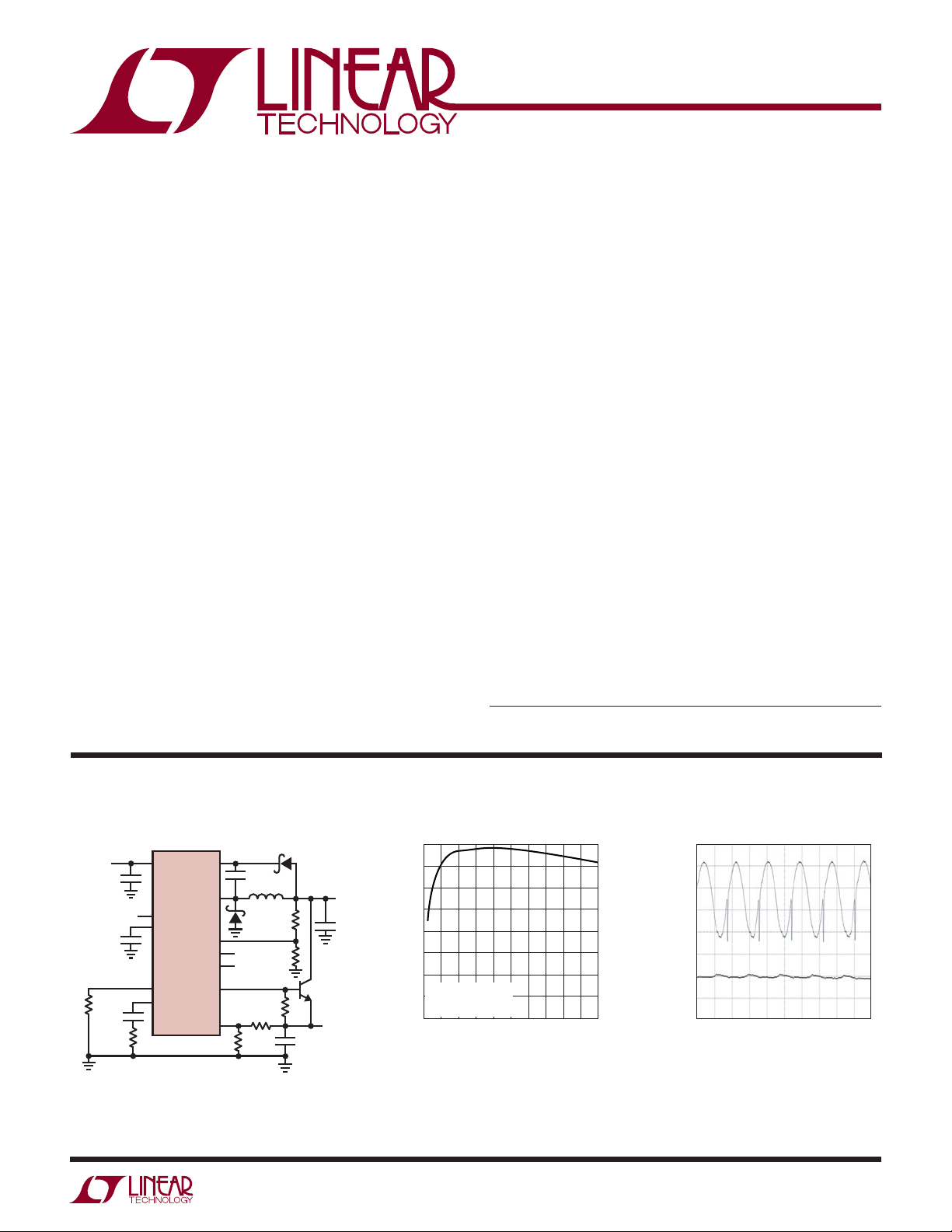
TYPICAL APPLICATION
Dual Step-Down Converters
6V TO 25V
0.47µF
53.6k
V
IN
2.2µF
330pF
40.2k
IN
SHDN
SS
R
T/
V
C
LT1939
SYNC
BSTV
SW
LDRV
LFB
FB
PG
PG
0.47µF
6.8µH
B240A
24.9k
8.06k
BAT54
42.2k
8.06k
1k
22µF
1939 TA01a
V
3.3V
1A
OUT2
V
5V
1A
22µF
OUT1
90
85
80
75
70
65
EFFICIENCY (%)
60
VIN = 12V
55
I
OUT2
FREQUENCY = 800kHz
50
0
= 0A
0.4 0.8 1.2 2.01.40.2 0.6 1.0 1.8
LOAD CURRENT (A)
1.6
1939 TA01b
V
V
OUT2
OUT1
= 5V AT 1A
AC COUPLED
2mV/DIV
= 3.3V AT 1A
AC COUPLED
2mV/DIV
Output Voltage RippleSwitching Converter Effi ciency
500ns/DIV
1939 TA01c
1939f
1
LT1939
(
PIN CONFIGURATIONABSOLUTE MAXIMUM RATINGS
(Note 1)
VIN, PG, PG Operating .................................... 25V/–0.3V
SW ............................................................................. V
IN
BST ................................................................ 45V/–0.3V
BST Pin Above SW ....................................................25V
LDRV, SHDN ..............................................................15V
FB, LFB, R
SS, V
/SYNC .......................................................5V
T
......................................................................2.5V
C
Operating Junction Temperature Range (Notes 2, 6)
LT1939EDD ........................................ –40°C to 125°C
V
IN
SHDN
SS
PG
V
RT/SYNC
12-LEAD
θJA = 45°C/W, θ
EXPOSED PAD (PIN 13) IS GND, MUST BE SOLDERED TO PCB
TOP VIEW
1
2
3
13
4
5
C
6
DD PACKAGE
3mm × 3mm) PLASTIC DFN
JC(PAD)
12
11
10
9
8
7
= 10°C/W
SW
BST
LDRV
LFB
FB
PG
LT1939IDD .........................................–40°C to 125°C
Storage Temperature Range ...................–65°C to 150°C
ORDER INFORMATION
LEAD FREE FINISH TAPE AND REEL PART MARKING* PACKAGE DESCRIPTION TEMPERATURE RANGE
LT1939EDD#PBF
LT1939IDD#PBF
Consult LTC Marketing for parts specifi ed with wider operating temperature ranges. *The temperature grade is identifi ed by a label on the shipping container.
Consult LTC Marketing for information on non-standard lead based fi nish parts.
For more information on lead free part marking, go to: http://www.linear.com/leadfree/
For more information on tape and reel specifi cations, go to: http://www.linear.com/tapeandreel/
LT1939EDD#TRPBF
LT1939IDD#TRPBF
LDJZ
LDJZ
12-Lead (3mm × 3mm) Plastic DFN
12-Lead (3mm × 3mm) Plastic DFN
–40°C to 125°C
–40°C to 125°C
The l denotes the specifi cations which apply over the full operating
ELECTRICAL CHARACTERISTICS
temperature range, otherwise specifi cations are at TJ = 25°C. V
= 15V, V
VIN
= 2V, unless otherwise specifi ed.
RT/SYNC
PARAMETER CONDITIONS MIN TYP MAX UNITS
l
SHDN Threshold
710 760 780 mV
SHDN Source Current 1.5 2.5 3.5 µA
SHDN Current Hysterisis 1.25 2 3.25 µA
Minimum Input Voltage (Note 3) V
Supply Shutdown Current V
Supply Quiescent Current V
FB Voltage V
FB Bias Current V
Error Amplifi er g
m
Error Amplifi er Source Current V
Error Amplifi er Sink Current V
Error Amplifi er High Clamp V
Error Amplifi er Switching Threshold V
SS Source Current V
= 0V
FB
= 0V
SHDN
= 0.9V 2.5 3.5 mA
FB
= 1V
VC
V
= 0.6V to 1.6V, VIN = 3V to 25V
VC
= 0.8V, VVC = 1V 50 150 nA
FB
VVC = 1V, IVC = ±10µA 150 250 350 µmho
= 0.6V, VVC = 1V 12 16 20 µA
FB
= 1V, VVC = 1V 14 18 22 µA
FB
= 0.6V 1.8 2.0 2.2 V
FB
= 0.6V 0.6 0.8 1.0 V
FB
= 1V, VSS = 0.4V, VFB = 0.9V 2.25 2.75 3.75 µA
SHDN
l
l
l
0.784
l
0.776
2.4 2.8 V
12 30 µA
0.8
0.8
0.816
0.824
1939f
V
V
2
LT1939
ELECTRICAL CHARACTERISTICS
The l denotes the specifi cations which apply over the full operating
temperature range, otherwise specifi cations are at T
= 25°C. V
J
PARAMETER CONDITIONS MIN TYP MAX UNITS
SS Sink Current V
SS POR Sink Current (Note 4) V
SS POR Threshold V
SS to FB Offset (V
– VFB)V
SS
PG/PG Leakage V
= 0V, VSS = 2V 300 600 900 µA
FB
= 0V, VSS = 2V, Cycle SHDN 400 600 800 µA
FB
= 0V 50 100 150 mV
FB
= 1V, VSS = 0.4V 70 100 120 mV
VC
= 0.9V/0.7V, VPG/VPG = 25V 0.1 1 µA
FB
PG/ PG Threshold VPG = 0.4V 0.685 0.708 0.730 V
PG/ PG Hysteresis V
PG Sink Current V
PG Sink Current V
/SYNC Reference Voltage V
R
T
Switching Frequency R
= 0.4V 20 30 40 mV
PG
= 0.4V, VFB = 0.7V 250 500 750 µA
PG
= 0.4V, VFB = 0.9V 500 800 1100 µA
PG
= 0.9V, R
FB1/2
RT/SYNC
R
RT/SYNC
R
RT/SYNC
RT/SYNC
= 90.9k
= 90.9k
= 15k
SYNC Frequency Range
Minimum Switch On Time V
Minimum Switch Off Time V
Switch Leakage Current V
Switch Saturation Voltage I
Switch Peak Current V
Boost Current ISW = 2A, V
Minimum Boost Voltage (Note 5) I
LFB Voltage V
LFB Line/Load Regulation V
– V
SS to LFB Offset (V
SS
)V
LFB
LFB Bias Current V
LDRV Dropout V
LDRV Maximum Current V
= 0.7V, R
FB
= 0.7V, R
FB
SW
= 2A, V
SW
BST
= 2A, VFB = 0.7V 2.2 3 V
SW
LDRV
VIN
= 1V, VSS = 0.8V, V
VC
LFB
LDRV
LDRV
RT/SYNC
RT/SYNC
= 0V 1 10 µA
= 18V, VFB = 0.7V 450 mV
BST
= 18V, VFB = 0.7V
= 18V, VFB = 0.7V 20 30 45 mA
BST
= 1.2V
= 3V to 25V, V
= 0.8V, VVC = 1V 115 300 nA
= 3V, I
LDRV
= 5mA
= 0V
= 15V, V
VIN
= 2V, unless otherwise specifi ed.
RT/SYNC
= 15k 0.75 0.850 0.975 V
450
l
425
2
l
250 2500 kHz
500
500
2.4
550
625
2.8
= 90.9k 140 ns
= 90.9k 120 ns
LDRV
= 8V
LDRV
= V
LFB
2.3
l
2.1
l
0.784 0.8 0.816 V
l
0.776 0.8 0.824 V
90 115 140 mV
l
0.8 1.2 1.6 V
l
91318mA
2.8
2.8
3.5
3.5
kHz
kHz
MHz
A
A
Note 1: Stresses beyond those listed under Absolute Maximum Ratings
may cause permanent damage to the device. Exposure to any Absolute
Maximum Rating condition for extended periods may affect device
reliability and lifetime.
Note2: The LT1939EDD is guaranteed to meet performance specifi cations
from 0°C to 125°C junction temperature. Specifi cations over the –40°C
to 125°C operating junction temperature range are assured by design,
characterization and correlation with statistical process controls. The
LT1939IDD is guaranteed over the full –40°C to 125°C operating junction
temperature range.
Note 3: Minimum input voltage is defi ned as the voltage where internal
bias lines are regulated so that the reference voltage and oscillator remain
constant. Actual minimum input voltage to maintain a regulated output
will depend upon output voltage and load current. See Applications
Information.
Note 4: An internal power-on reset (POR) latch is set on the positive
transition of the SHDN pin through its threshold. The output of the latch
activates a current source on the SS pin which typically sinks 600µA,
discharging the SS capacitor. The latch is reset when the SS pin is driven
below the soft-start POR threshold or the SHDN pin is taken below its
threshold.
Note 5: This is the minimum voltage across the boost capacitor needed to
guarantee full saturation of the internal power switch.
Note 6: This IC includes overtemperature protection that is intended
to protect the device during momentary overload conditions. Junction
temperature will exceed the maximum operating junction temperature
when overtemperature protection is active. Continuous operation above
the specifi ed maximum operating junction temperature may impair device
reliability.
1939f
3
LT1939
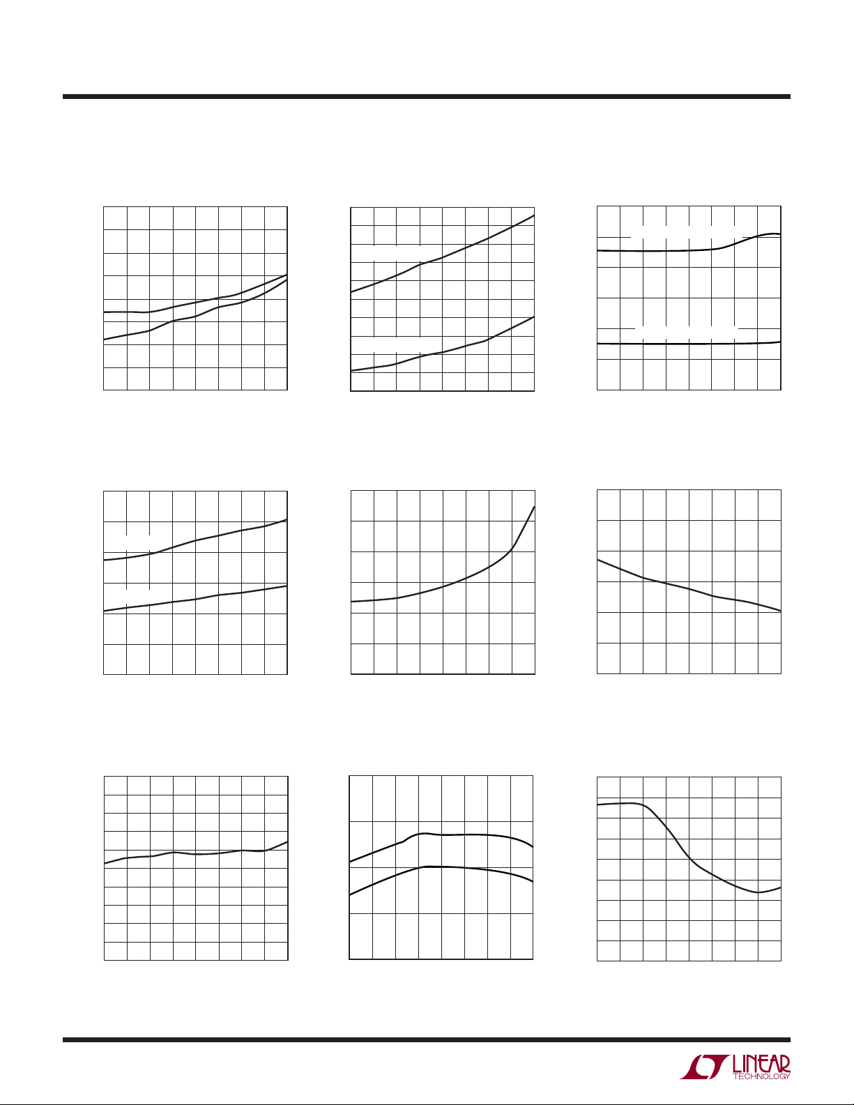
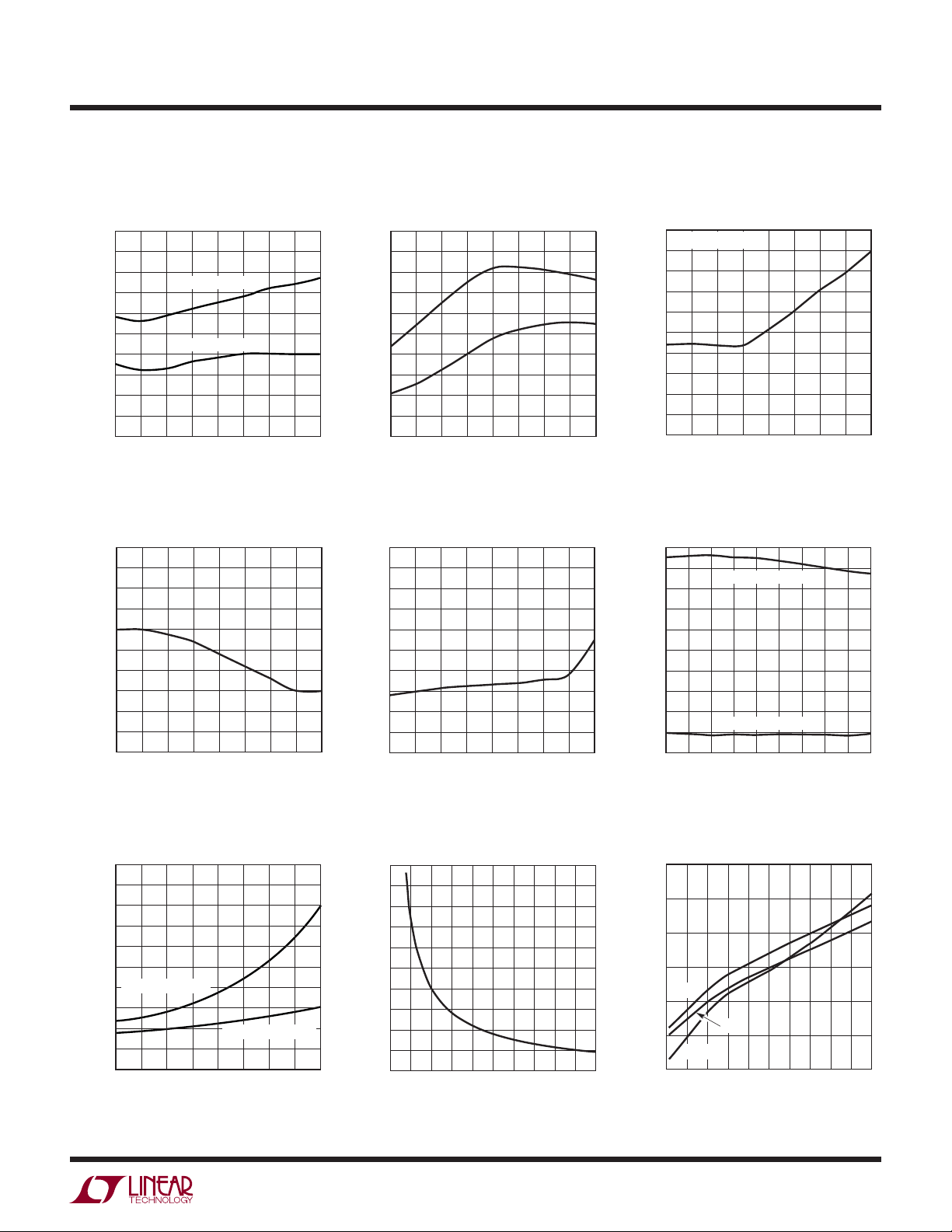
TYPICAL PERFORMANCE CHARACTERISTICS
Feedback Voltage vs Temperature
0.820
0.815
0.810
0.805
0.800
VOLTAGE (V)
0.795
0.790
0.785
0.780
–50
–25
0
TEMPERATURE (°C)
FB
50
25
75
LFB
100
125
150
1939 G01
R
/SYNC Voltage vs Temperature
T
1.10
1.08
1.06
R
= 90.9k
R
–50
–25 25
RT/SYNC
= 15k
RT/SYNC
0
TEMPERATURE (°C)
50
1.04
1.02
1.00
0.98
VOLTAGE (V)
0.96
0.94
0.92
0.90
100
75
125
1939 G02
150
Shutdown Threshold and Minimum
Input Voltage vs Temperature
3.0
2.5
2.0
1.5
VOLTAGE (V)
1.0
0.5
0
–50
MINIMUM INPUT VOLTAGE
SHUTDOWN THRESHOLD
50 100 150125
–25 0
25 75
TEMPERATURE (°C)
1939 G03
Shutdown Pin Currents vs
Temperature
6
5
V
= 0.9V
SHDN
4
3
V
= 0.7V
SHDN
CURRENT (µA)
2
1
0
–50
050
–25 25
TEMPERATURE (°C)
Soft-Start Source Current vs
Temperature
3.5
3.3
3.1
2.9
2.7
2.5
2.3
CURRENT (µA)
2.1
1.9
1.7
1.5
–50
–25 25
0
50
TEMPERATURE (°C)
Shutdown Quiescent Current vs
Temperature
15.0
12.5
10.0
7.5
CURRENT (µA)
5.0
2.5
0
100
75
125
150
1939 G04
–50
050
–25 25
TEMPERATURE (°C)
100
75
125
150
1939 G05
Soft-Start Feedback Offset vs
Temperature
150
125
LFB
100
VOLTAGE (mV)
75
125
100
75
150
1939 G07
50
FB
–50
–25 0 25 50
TEMPERATURE (°C)
75 100 125 150
1939 G08
Error Amplifi er g
400
350
300
250
200
TRANSCONDUCTANCE (µmhos)
150
100
–25 25
–50
050
TEMPERATURE (°C)
VC Switching Threshold vs
Temperature
0.95
0.90
0.85
0.80
0.75
0.70
VOLTAGE (V)
0.65
0.60
0.55
0.50
–50
–25
0
TEMPERATURE (°C)
vs Temperature
m
75
100
125
25 150125
50
75 100
150
1939 G06
1939 G09
4
1939f
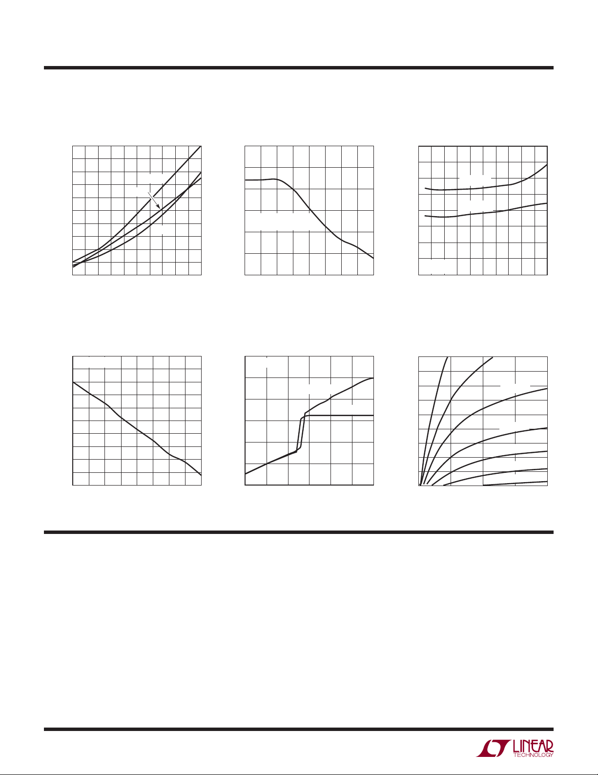
TYPICAL PERFORMANCE CHARACTERISTICS
LT1939
Power Good Thresholds vs
Temperature
0.75
0.74
0.73
0.72
0.71
0.70
0.69
VOLTAGE (V)
0.68
0.67
0.66
0.65
–50
–25
RISING EDGE
FALLING EDGE
25
0
TEMPERATURE (°C)
Peak Switch Current vs
Temperature
3.5
3.4
3.3
3.2
3.1
3.0
2.9
CURRENT (A)
2.8
2.7
2.6
2.5
–50
–25
25
0
TEMPERATURE (°C)
Power Good Sink Currents vs
Temperature Frequency vs Temperature
1000
900
800
700
600
500
400
CURRENT (µA)
300
200
100
50
75
100
150125
1939 G10
0
–50
–25
PG
PG
50
25
0
TEMPERATURE (°C)
75
100
150125
1939 G11
LDRV Short-Circuit Current vs
Temperature
20
19
18
17
16
15
14
CURRENT (mA)
13
12
11
50
75
100
150125
1939 G13
10
–50
–25
0
50
25
TEMPERATURE (°C)
75
100
150125
1939 G14
600
R
= 90.9k
RT/SYNC
580
560
540
520
500
480
FREQUENCY (kHz)
460
440
420
400
–50
–25
0
50
25
TEMPERATURE (°C)
75
External Sync Duty Cycle Range
vs External Sync Frequency
100
90
80
70
60
50
40
DUTY CYCLE (%)
30
20
10
0
250
MAXIMUM DUTY CYCLE
MINIMUM DUTY CYCLE
750
SYNCHRONIZATION FREQUENCY (kHz)
1250
1750
100
150125
1939 G12
2250
19939 G15
Minimum Switching Times Frequency vs R
300
275
250
225
200
175
TIME (ns)
150
125
100
75
50
–50
MINIMUM ON TIME
–25 25
0
TEMPERATURE (°C)
MINIMUM OFF TIME
50
100
75
125
150
1939 G16
2500
2250
2000
1750
1500
1250
1000
FREQUENCY (kHz)
750
500
250
0
0
Switch Saturation Voltage vs
RT/SYNC
4020
8060
R
RT/SYNC
120 140 180
100
(kΩ)
160
200
1939 G17
Switch Current
600
500
400
300
–50°C
200
100
SWITCH SATURATION VOLTAGE (mV)
0
25°C
150°C
0.4 0.8 1.2 1.6
SWITCH CURRENT (A)
2.00.20 0.6 1.0 1.4 1.8
1939 G18
1939f
5
LT1939
TYPICAL PERFORMANCE CHARACTERISTICS
Minimum Boost Voltages vs
Boost Current vs Switch Current
50
45
40
35
30
25
20
15
BOOST CURRENT (mA)
10
5
0
0.40.2
0
SWITCH CURRENT (A)
–50°C
0.80.6
1.0
150°C
1.2 1.4 1.8
LDRV Dropout Voltage vs
Temperature
1.50
I
= 5mA
LDRV
1.45
1.40
1.35
1.30
1.25
1.20
VOLTAGE (V)
1.15
1.10
1.05
1.00
–50
–25 25
0
50
TEMPERATURE (°C)
25°C
75
100
1.6
125
2.0
1939 G19
150
1939 G22
Temperature Minimum Input Voltage
2.7
2.5
2.3
2.1
MINIMUM BOOST FOR
SWITCH SATURATION
1.9
BOOST VOLTAGE (V)
1.7
1.5
–50
050
–25 25
TEMPERATURE (°C)
100
75
Switcher Dropout Operation
6
I
= 1A
OUT1
5
V
= 5V
4
3
2
OUTPUT VOLTAGE (V)
1
0
2.5
3.0
INPUT VOLTAGE (V)
OUT1
3.5 4.0 4.5
V
OUT1
150
125
1939 G20
= 3.3V
5.0 5.5
1939 G23
8
7
6
5
4
3
INPUT VOLTAGE (V)
2
1
FSW = 1MHz
L = 3.3µH
0
0
V
= 5V
OUT1
V
= 3.3V
OUT1
0.4 0.8 1.2 2.01.40.2 0.6 1.0 1.8
LOAD CURRENT (A)
Inductor Value for 2A Maximum
Load Current (V
I
RIPPLE
2500
L = 1µH
2250
2000
1750
1500
1250
1000
FREQUENCY (kHz)
750
500
250
5
= 250mA)
L = 1.5µH
10
INPUT VOLTAGE (V)
OUT
15
= 3.3V,
1.6
1939 G21
L = 2.2µH
L = 3.3µH
L = 4.7µH
L = 6.8µH
L = 10µH
20 25
1939 G24
PIN FUNCTIONS
VIN (Pin 1): The VIN pin powers the internal control circuitry
and is monitored by an undervoltage comparator. The V
IN
pin is also connected to the collectors of the internal power
NPN switch and linear output NPN. The V
pin has high
IN
dI/dt edges and must be decoupled to ground close to
the pin of the device.
SHDN (Pin 2): The SHDN pin is used to shut down the
LT1939 and reduce quiescent current to a typical value
of 12µA. The accurate 0.76V threshold and input current
6
hysteresis can be used as an undervoltage lockout, preventing the regulator from operating until the input voltage has
reached a predetermined level. Force the SHDN pin above
its threshold or let it fl oat for normal operation.
SS (Pin 3): The SS pin is used to control the slew rate
of the output of both the switching and linear regulators.
A single capacitor from the SS pin to ground determines
the regulators’ ramp rate. For soft-start details see the
Applications Information section.
1939f

PIN FUNCTIONS
LT1939
PG (Pin 4): The power good pin is an open-collector
output that sinks current when the FB or LFB falls below
90% of its nominal regulating voltage. For V
its output state remains true, although during SHDN, V
above 2V,
IN
IN
undervoltage lockout, or thermal shutdown, its current
sink capability is reduced.
(Pin 5): The VC pin is the output of the error amplifi er
V
C
and the input to the peak switch current comparator. It is
normally used for frequency compensation, but can also
be used as a current clamp or control loop override. If
the error amplifi er drives V
above the maximum switch
C
current level, a voltage clamp activates. This indicates that
the output is overloaded and current to be pulled from the
SS pin reducing the regulation point.
/SYNC (Pin 6): This RT/SYNC pin provides two modes
R
T
of setting the constant switch frequency.
Connecting a resistor from the R
will set the R
/SYNC pin to a typical value of 1V. The
T
/SYNC pin to ground
T
resultant switching frequency will be set by the resistor
value. The minimum value of 15k and maximum value
of 200k set the switching frequency to 2.5MHz and
250kHz respectively.
Driving the R
/SYNC pin with an external clock signal
T
will synchronize the switch to the applied frequency.
Synchronization occurs on the rising edge of the clock
signal after the clock signal is detected. Each rising clock
edge initiates an oscillator ramp reset. A gain control loop
servos the oscillator charging current to maintain a constant oscillator amplitude. Hence, the slope compensation
remains unchanged. If the clock signal is removed, the
oscillator reverts to resistor mode and reapplies the 1V
bias to the R
/SYNC pin after the synchronization detection
T
circuitry times out. The clock source impedance should
be set such that the current out of the R
/SYNC pin in
T
resistor mode generates a frequency roughly equivalent
to the synchronization frequency. Floating or holding the
/SYNC pin above 1.1V will not damage the device, but
R
T
will halt oscillation.
PG (Pin 7): The power good bar pin is an open-collector
output that sinks current when the FB or LFB rises above
90% of its nominal regulating voltage.
FB (Pin 8): The FB pin is the negative input to the switcher
error amplifi er. The output switches to regulate this pin to
0.8V with respect to the exposed ground pad. Bias current
fl ows out of the FB pin.
LFB (Pin 9): The LFB pin is the negative input to the linear
error amplifi er. The L
pin servo’s to regulate this pin to
DRV
0.8V with respect to the exposed ground pad. Bias current
fl ows out of the LFB pin.
LDRV (Pin 10): The LDRV pin is the emitter of an internal NPN that can be confi gured as an output of a linear
regulator or as the drive for an external NPN high current
regulator. Current fl ows out of the LDRV pin when the
LFB pin voltage is below 0.8V. The LDRV pin has a typical
maximum current capability of 13mA.
BST (Pin 11): The BST pin provides a higher than V
base
IN
drive to the power NPN to ensure a low switch drop. A
comparator to V
imposes a minimum off time on the SW
IN
pin if the BST pin voltage drops too low. Forcing a SW off
time allows the boost capacitor to recharge.
SW (Pin 12): The SW pin is the emitter of the on-chip
power NPN. At switch off, the inductor will drive this pin
below ground with a high dV/dt. An external catch diode to
ground, close to the SW pin and respective V
decoupling
IN
capacitor’s ground, must be used to prevent this pin from
excessive negative voltages.
Exposed Pad (Pin 13): GND. The Exposed Pad is the
only ground connection for the device. The Exposed Pad
should be soldered to a large copper area to reduce thermal resistance. The GND pin also serves as small-signal
ground. For ideal operation all small-signal ground paths
should connect to the GND pin at a single point, avoiding
any high current ground returns.
1939f
7

LT1939
–
+
–
+
+
–
+
+
–
+
–
–
+
1
INTERNAL
REGULATOR
AND REFERENCES
OSCILLATOR
AND AGC
POWER ON RESET
THERMAL
OVERLOAD
SQR
PRE
SQR
2µA
2.75µA
2.5µA
C1
0.76V
–
+
100mV
R5
R6
V
IN
13
GND
2
10
11
SHDN
6
R
T
/SYNC
5
V
C
3
SS
DRIVER
CIRCUITRY
SLOPE
COMPENSATION
0.8V
SS
115mV
LDRV
R3
R1
R2
R4
C5
D2
D1
V
OUT2
V
OUT1
1939 BD
9
LFB
BST
12
SW
8
FB
4
PG
PG
0.8V
100mV
0.7V
LFB
SS
7
C6
L1
C2
C4C3
C7
+
+
BLOCK DIAGRAM
Figure 1. LT1939 Block Diagram
8
1939f
 Loading...