

LT1930/LT1930A
1A, 1.2MHz/2.2MHz,
Step-Up DC/DC Converters
FEATURES
■
1.2MHz Switching Frequency (LT1930)
■
2.2MHz Switching Frequency (LT1930A)
■
Low V
■
High Output Voltage: Up to 34V
■
5V at 480mA from 3.3V Input (LT1930)
■
12V at 250mA from 5V Input (LT1930A)
■
Wide Input Range: 2.6V to 16V
■
Uses Small Surface Mount Components
■
Low Shutdown Current: <1µA
■
Low Profile (1mm) ThinSOTTM Package
■
Pin-for-Pin Compatible with the LT1613
Switch: 400mV at 1A
CESAT
U
APPLICATIO S
■
TFT-LCD Bias Supply
■
Digital Cameras
■
Cordless Phones
■
Battery Backup
■
Medical Diagnostic Equipment
■
Local 5V or 12V Supply
■
External Modems
■
PC Cards
■
xDSL Power Supply
, LTC and LT are registered trademarks of Linear Technology Corporation
ThinSOT is a trademark of Linear Technology Corporation.
U
in ThinSOT
DESCRIPTIO
The LT®1930 and LT1930A
power SOT-23 switching regulators. Both include an
internal 1A, 36V switch allowing high current outputs to be
generated in a small footprint. The LT1930 switches at
1.2MHz, allowing the use of tiny, low cost and low height
capacitors and inductors. The faster LT1930A switches at
2.2MHz, enabling further reductions in inductor size.
Complete regulator solutions approaching one tenth of a
square inch in area are achievable with these devices.
Multiple output power supplies can now use a separate
regulator for each output voltage, replacing cumbersome
quasi-regulated approaches using a single regulator and
custom transformers.
A constant frequency internally compensated current mode
PWM architecture results in low, predictable output noise
that is easy to filter. Low ESR ceramic capacitors can be
used at the output, further reducing noise to the millivolt
level. The high voltage switch on the LT1930/LT1930A is
rated at 36V, making the device ideal for boost converters
up to 34V as well as for single-ended primary inductance
converter (SEPIC) and flyback designs. The LT1930 can
generate 5V at up to 480mA from a 3.3V supply or 5V at
300mA from four alkaline cells in a SEPIC design.
The LT1930/LT1930A are available in the 5-lead ThinSOT
package.
are the industry’s highest
U
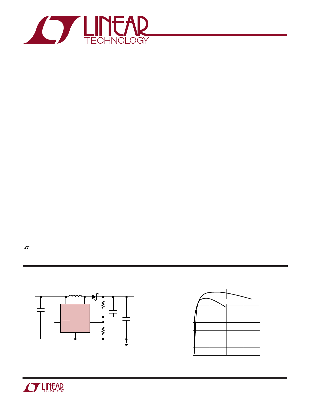
TYPICAL APPLICATIO
L1
V
IN
5V
C1
2.2µF
SHDN
C1: TAIYO-YUDEN X5R LMK212BJ225MG
C2: TAIYO-YUDEN X5R EMK316BJ475ML
D1: ON SEMICONDUCTOR MBR0520
L1: SUMIDA CR43-100
*OPTIONAL
10µH
51
V
IN
LT1930
4
SHDN FB
GND
2
Figure 1. 5V to 12V, 300mA Step-Up DC/DC Converter
SW
D1
R1
113k
3
R2
13.3k
C3*
10pF
V
12V
300mA
C2
4.7µF
1930/A F01
OUT
90
85
80
75
70
65
EFFICIENCY (%)
60
55
50
0
Efficiency
VIN = 3.3V
100
200
LOAD CURRENT (mA)
VIN = 5V
300
400
1930 TA01
1
LT1930/LT1930A
PACKAGE/ORDER I FOR ATIO
UU
W
WWWU
ABSOLUTE AXI U RATI GS
(Note 1)
VIN Voltage .............................................................. 16V
SW Voltage ................................................–0.4V to 36V
FB Voltage .............................................................. 2.5V
Current Into FB Pin .............................................. ±1mA
SHDN Voltage ......................................................... 10V
Maximum Junction Temperature ......................... 125°C
Operating Temperature Range (Note 2) .. –40°C to 85°C
Storage Temperature Range ................. –65°C to 150°C
Lead Temperature (Soldering, 10 sec)..................300°C
TOP VIEW
SW 1
GND 2
FB 3
S5 PACKAGE
5-LEAD PLASTIC SOT-23
T
= 125°C, θJA = 256°C/W
JMAX
Consult LTC Marketing for parts specified with wider operating temperature ranges.
5 V
IN
4 SHDN
ORDER PART
NUMBER
LT1930ES5
LT1930AES5
S5 PART MARKING
LTKS
LTSQ
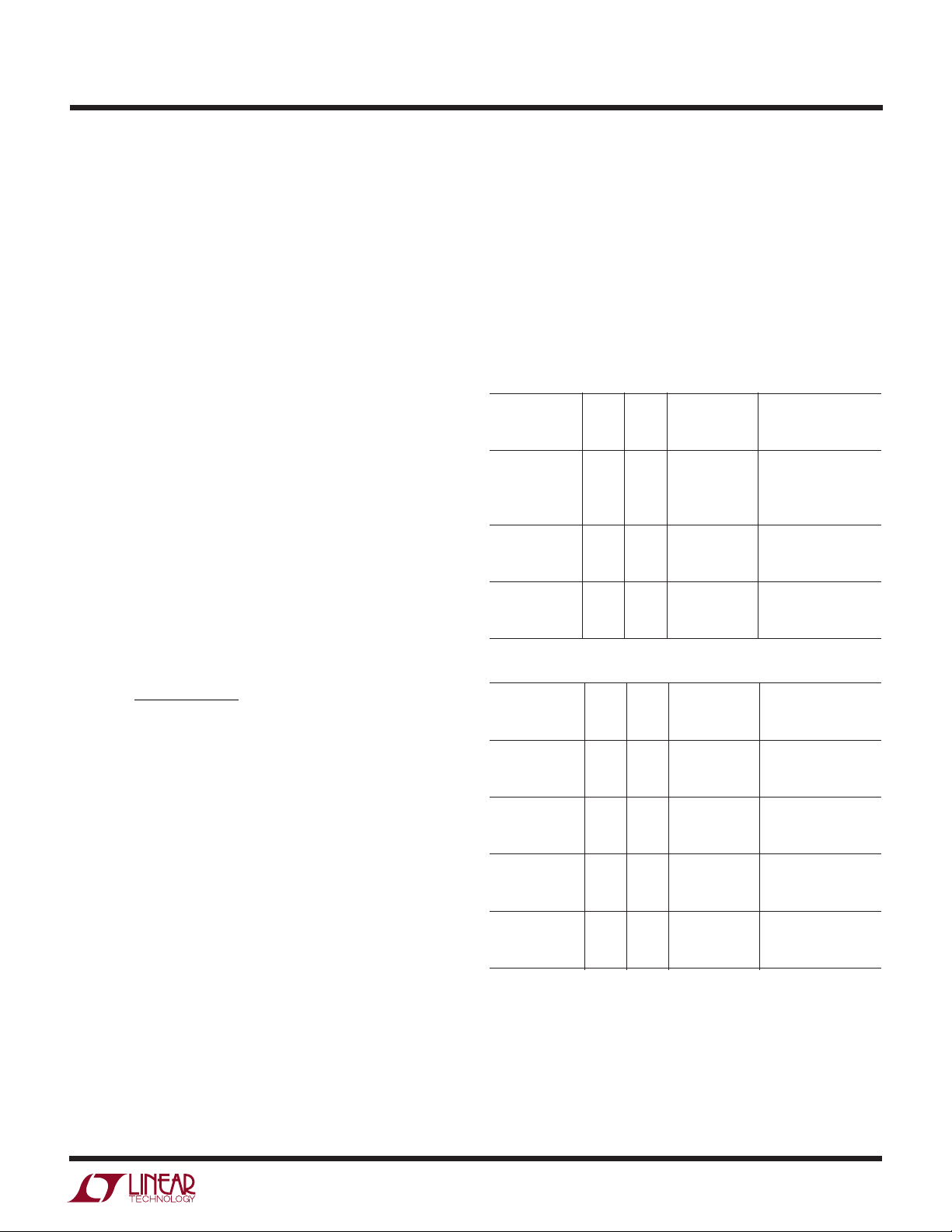
ELECTRICAL CHARACTERISTICS
The ● denotes specifications which apply over the full operating temperature range, otherwise specifications are TA = 25°C.
VIN = 3V, V
PARAMETER CONDITIONS MIN TYP MAX MIN TYP MAX UNITS
Minimum Operating Voltage 2.45 2.6 2.45 2.6 V
Maximum Operating Voltage 16 16 V
Feedback Voltage 1.240 1.255 1.270 1.240 1.255 1.270 V
FB Pin Bias Current VFB = 1.255V ● 120 360 240 720 nA
Quiescent Current V
Quiescent Current in Shutdown V
Reference Line Regulation 2.6V ≤ VIN ≤ 16V 0.01 0.05 0.01 0.05 %/V
Switching Frequency 1 1.2 1.4 1.8 2.2 2.6 MHz
Maximum Duty Cycle ● 84 90 75 90 %
Switch Current Limit (Note 3) 1 1.2 2 1 1.2 2.5 A
Switch V
CESAT
Switch Leakage Current VSW = 5V 0.01 1 0.01 1 µA
SHDN Input Voltage High 2.4 2.4 V
SHDN Input Voltage Low 0.5 0.5 V
SHDN Pin Bias Current V
Note 1: Absolute Maximum Ratings are those values beyond which the life
of a device may be impaired.
Note 2: The LT1930E/LT1930AE are guaranteed to meet performance
specifications from 0°C to 70°C. Specifications over the –40°C to 85°C
= VIN unless otherwise noted. (Note 2)
SHDN
= 2.4V, Not Switching 4.2 6 5.5 8 mA
SHDN
= 0V, VIN = 3V 0.01 1 0.01 1 µA
SHDN
ISW = 1A 400 600 400 600 mV
= 3V 16 32 35 70 µA
SHDN
= 0V 0 0.1 0 0.1 µA
V
SHDN
LT1930 LT1930A
● 1.230 1.280 1.230 1.280 V
● 0.85 1.6 1.6 2.9 MHz
operating temperature range are assured by design, characterization and
correlation with statistical process controls.
Note 3: Current limit guaranteed by design and/or correlation to static test.
2
LT1930/LT1930A
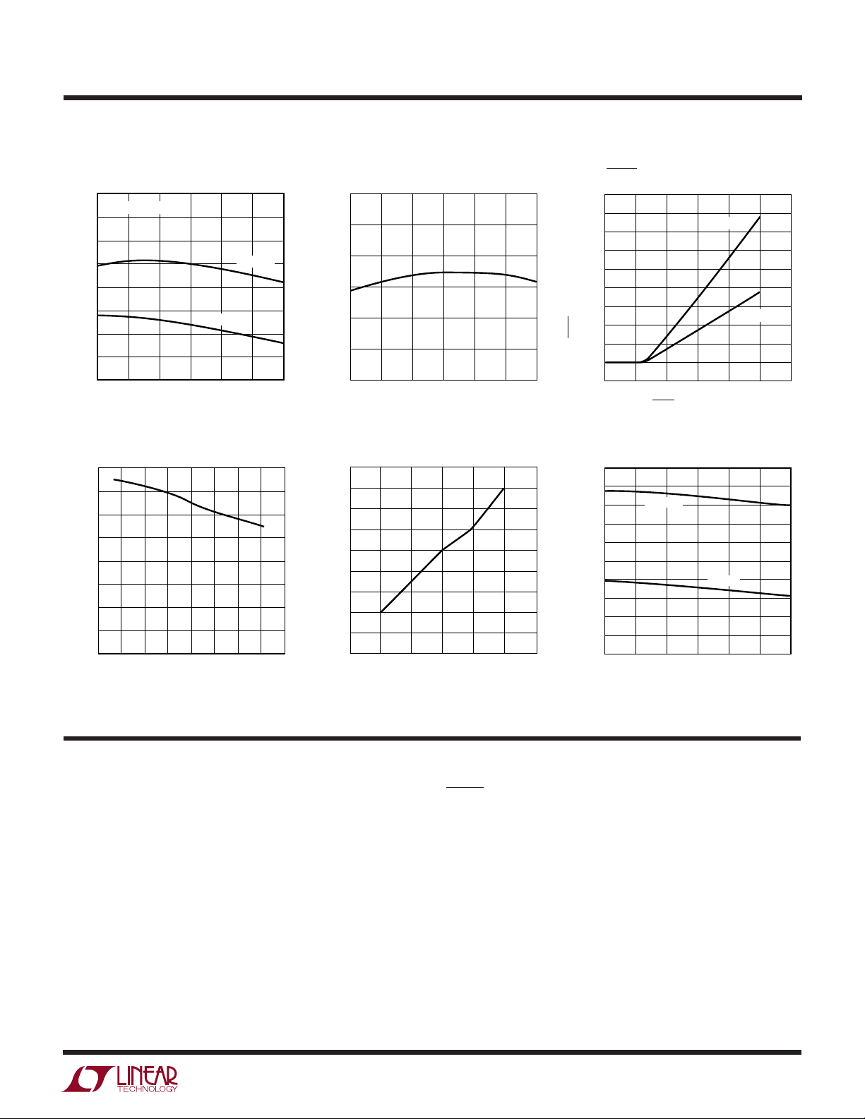
UW
TYPICAL PERFOR A CE CHARACTERISTICS
Quiescent Current FB Pin Voltage SHDN Pin Current
7.0
NOT SWITCHING
6.5
6.0
5.5
5.0
4.5
4.0
QUIESCENT CURRENT (mA)
3.5
3.0
–50 –25
0 25 100
TEMPERATURE (°C)
LT1930A
LT1930
50 75
1930/A G01
1.28
1.27
1.26
1.25
FB VOLTAGE (V)
1.24
1.23
1.22
–50
–25
02550
TEMPERATURE (°C)
75 100
1930/A G02
90
80
70
60
50
40
30
20
SHDN PIN CURRENT (µA)
10
0
–10
0
LT1930A
LT1930
12 4
SHDN PIN VOLTAGE (V)
3
5
1930/A G03
6
Current Limit
1.6
1.4
1.2
1.0
0.8
0.6
CURRENT LI MIT (A)
0.4
0.2
0
10
3020 5040 7060 9080
U
DUTY CYCLE (%)
1930/A G04
UU
Switch Saturation Voltage
0.45
0.40
0.35
0.30
0.25
(V)
0.20
CESAT
V
0.15
0.10
0.05
0
0
0.4 1.2
0.2 1.0
SWITCH CURRENT (A)
PI FU CTIO S
SW (Pin 1): Switch Pin. Connect inductor/diode here.
Minimize trace area at this pin to reduce EMI.
GND (Pin 2): Ground. Tie directly to local ground plane.
Oscillator Frequency
2.5
2.3
LT1930A
LT1930
25 50 75 100
TEMPERATURE (°C)
1930/A G06
0.6
0.8
1930/A G05
2.1
1.9
1.7
1.5
1.3
FREQUENCY (MHz)
1.1
0.9
0.7
0.5
–50 –25 0
SHDN (Pin 4): Shutdown Pin. Tie to 2.4V or more to enable
device. Ground to shut down.
V
(Pin 5): Input Supply Pin. Must be locally bypassed.
IN
FB (Pin 3): Feedback Pin. Reference voltage is 1.255V.
Connect resistive divider tap here. Minimize trace area at
FB. Set V
according to V
OUT
= 1.255V(1 + R1/R2).
OUT
3

LT1930/LT1930A
BLOCK DIAGRA
V
IN
5
V
OUT
R1 (EXTERNAL)
FB
R2 (EXTERNAL)
W
1.255V
REFERENCE
1
+
A1
–
R
C
C
C
COMPARATOR
–
A2
+
RQ
S
DRIVER
SW
Q1
+
Σ
0.01Ω
–
RAMP
GENERATOR
SHUTDOWN
SHDN
4
FB
3
Figure 2. Block Diagram
U
OPERATIO
The LT1930 uses a constant frequency, current-mode
control scheme to provide excellent line and load regulation. Operation can be best understood by referring to the
block diagram in Figure 2. At the start of each oscillator
cycle, the SR latch is set, which turns on the power switch
Q1. A voltage proportional to the switch current is added
to a stabilizing ramp and the resulting sum is fed into the
positive terminal of the PWM comparator A2. When this
voltage exceeds the level at the negative input of A2, the SR
latch is reset turning off the power switch. The level at the
negative input of A2 is set by the error amplifier A1, and is
simply an amplified version of the difference between the
feedback voltage and the reference voltage of 1.255V. In
2
GND
1.2MHz
OSCILLATOR*
*2.2MHz FOR LT1930A
1930/A BD
this manner, the error amplifier sets the correct peak
current level to keep the output in regulation. If the error
amplifier’s output increases, more current is delivered to
the output; if it decreases, less current is delivered. The
LT1930 has a current limit circuit not shown in Figure 2.
The switch current is constantly monitored and not allowed to exceed the maximum switch current (typically
1.2A). If the switch current reaches this value, the SR latch
is reset regardless of the state of comparator A2. This
current limit helps protect the power switch as well as the
external components connected to the LT1930.
The block diagram for the LT1930A (not shown) is identical except that the oscillator frequency is 2.2MHz.
4
LT1930/LT1930A
U
WUU
APPLICATIONS INFORMATION
LT1930 AND LT1930A DIFFERENCES
Switching Frequency
The key difference between the LT1930 and LT1930A is
the faster switching frequency of the LT1930A. At 2.2MHz,
the LT1930A switches at nearly twice the rate of the
LT1930. Care must be taken in deciding which part to use.
The high switching frequency of the LT1930A allows
smaller cheaper inductors and capacitors to be used in a
given application, but with a slight decrease in efficiency
and maximum output current when compared to the
LT1930. Generally, if efficiency and maximum output
current are critical, the LT1930 should be used. If application size and cost are more important, the LT1930A will be
the better choice. In many applications, tiny inexpensive
chip inductors can be used with the LT1930A, reducing
solution cost.
Duty Cycle
The maximum duty cycle (DC) of the LT1930A is 75%
compared to 84% for the LT1930. The duty cycle for a
given application using the boost topology is given by:
VV
||–||
DC
For a 5V to 12V application, the DC is 58.3% indicating that
the LT1930A could be used. A 5V to 24V application has
a DC of 79.2% making the LT1930 the right choice. The
LT1930A can still be used in applications where the DC, as
calculated above, is above 75%. However, the part must
be operated in the discontinuous conduction mode so that
the actual duty cycle is reduced.
INDUCTOR SELECTION
Several inductors that work well with the LT1930 are listed
in Table 1 and those for the LT1930A are listed in Table 2.
These tables are not complete, and there are many other
manufacturers and devices that can be used. Consult each
manufacturer for more detailed information and for their
entire selection of related parts, as many different sizes and
shapes are available. Ferrite core inductors should be used
to obtain the best efficiency, as core losses at 1.2MHz are
much lower for ferrite cores than for cheaper powdered-
OUT IN
=
V
||
OUT
iron types. Choose an inductor that can handle at least 1A
without saturating, and ensure that the inductor has a low
DCR (copper-wire resistance) to minimize I2R power losses.
A 4.7µH or 10µH inductor will be the best choice for most
LT1930 designs. For LT1930A designs, a 2.2µH to 4.7µH
inductor will usually suffice. Note that in some applications, the current handling requirements of the inductor
can be lower, such as in the SEPIC topology where each
inductor only carries one-half of the total switch current.
Table 1. Recommended Inductors – LT1930
MAX SIZE
L DCR L × W × H
PART (µH) mΩ (mm) VENDOR
CDRH5D18-4R1 4.1 57 4.5 × 4.7 × 2.0 Sumida
CDRH5D18-100 10 124 (847) 956-0666
CR43-4R7 4.7 109 3.2 × 2.5 × 2.0 www.sumida.com
CR43-100 10 182
DS1608-472 4.7 60 4.5 × 6.6 × 2.9 Coilcraft
DS1608-103 10 75 (847) 639-6400
www.coilcraft.com
ELT5KT4R7M 4.7 240 5.2 × 5.2 × 1.1 Panasonic
ELT5KT6R8M 6.8 360 (408) 945-5660
www.panasonic.com
Table 2. Recommended Inductors – LT1930A
MAX SIZE
L DCR L × W × H
PART (µH) mΩ (mm) VENDOR
LQH3C2R2M24 2.2 126 3.2 × 2.5 × 2.0 Murata
LQH3C4R7M24 4.7 195 (404) 573-4150
www.murata.com
CR43-2R2 2.2 71 4.5 × 4.0 × 3.0 Sumida
CR43-3R3 3.3 86 (847) 956-0666
www.sumida.com
1008PS-272 2.7 100 3.7 × 3.7 × 2.6 Coilcraft
1008PS-332 3.3 110 (800) 322-2645
www.coilcraft.com
ELT5KT3R3M 3.3 204 5.2 × 5.2 × 1.1 Panasonic
(408) 945-5660
www.panasonic.com
The inductors shown in Table 2 for use with the LT1930A
were chosen for small size. For better efficiency, use
similar valued inductors with a larger volume. For
example, the Sumida CR43 series in values ranging from
2.2µH to 4.7µH will give an LT1930A application a few
percentage points increase in efficiency, compared to the
smaller Murata LQH3C Series.
5

LT1930/LT1930A
U
WUU
APPLICATIONS INFORMATION
CAPACITOR SELECTION
Low ESR (equivalent series resistance) capacitors should
be used at the output to minimize the output ripple voltage.
Multi-layer ceramic capacitors are an excellent choice, as
they have extremely low ESR and are available in very
small packages. X5R dielectrics are preferred, followed by
X7R, as these materials retain the capacitance over wide
voltage and temperature ranges. A 4.7µF to 10µF output
capacitor is sufficient for most applications, but systems
with very low output currents may need only a 1µF or 2.2µF
output capacitor. Solid tantalum or OSCON capacitors can
be used, but they will occupy more board area than a
ceramic and will have a higher ESR. Always use a capacitor
with a sufficient voltage rating.
Ceramic capacitors also make a good choice for the input
decoupling capacitor, which should be placed as close as
possible to the LT1930/LT1930A. A 1µF to 4.7µF input
capacitor is sufficient for most applications. Table 3 shows
a list of several ceramic capacitor manufacturers. Consult
the manufacturers for detailed information on their entire
selection of ceramic parts.
Table 3. Ceramic Capacitor Manufacturers
Taiyo Yuden (408) 573-4150 www.t-yuden.com
AVX (803) 448-9411 www.avxcorp.com
Murata (714) 852-2001 www.murata.com
By choosing the appropriate values for the resistor and
capacitor, the zero frequency can be designed to improve
the phase margin of the overall converter. The typical
target value for the zero frequency is between 35kHz to
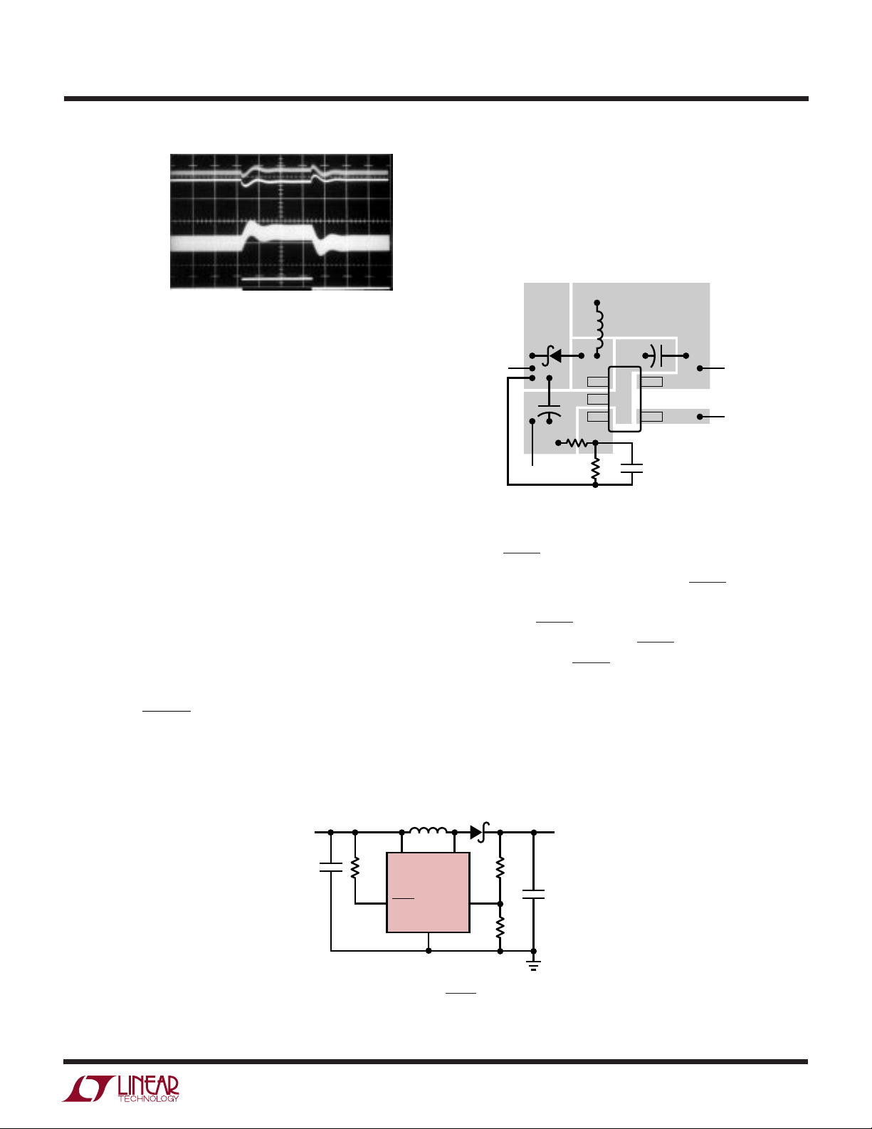
55kHz. Figure 3 shows the transient response of the stepup converter from Figure 1 without the phase lead capacitor C3. The phase margin is reduced as evidenced by more
ringing in both the output voltage and inductor current. A
10pF capacitor for C3 results in better phase margin,
which is revealed in Figure 4 as a more damped response
and less overshoot. Figure 5 shows the transient response
when a 33µF tantalum capacitor with no phase lead
capacitor is used on the output. The higher output voltage
ripple is revealed in the upper waveform as a set of double
lines. The transient response is not greatly improved
which implies that the ESR zero frequency is too high to
increase the phase margin.
V
OUT
0.2V/DIV
AC COUPLED
I
LI
0.5A/DIV
AC COUPLED
250mA
LOAD
CURRENT
150mA
50µs/DIV
1930 F03
The decision to use either low ESR (ceramic) capacitors or
the higher ESR (tantalum or OSCON) capacitors can affect
the stability of the overall system. The ESR of any capacitor, along with the capacitance itself, contributes a zero to
the system. For the tantalum and OSCON capacitors, this
zero is located at a lower frequency due to the higher value
of the ESR, while the zero of a ceramic capacitor is at a
much higher frequency and can generally be ignored.
A phase lead zero can be intentionally introduced by
placing a capacitor (C3) in parallel with the resistor (R1)
between V
and VFB as shown in Figure 1. The frequency
OUT
of the zero is determined by the following equation.
ƒ=
Z
1
RC
213π••
6
Figure 3. Transient Response of Figure 1's Step-Up
Converter without Phase Lead Capacitor
V
OUT
0.2V/DIV
AC COUPLED
I
LI
0.5A/DIV
AC COUPLED
250mA
LOAD
CURRENT
150mA
50µs/DIV
Figure 4. Transient Response of Figure 1's Step-Up
Converter with 10pF Phase Lead Capacitor
1930 F04
LT1930/LT1930A
U
WUU
APPLICATIONS INFORMATION
V
OUT
0.2V/DIV
AC COUPLED
I
LI
0.5A/DIV
AC COUPLED
LOAD
250mA
CURRENT
Figure 5. Transient Response of Step-Up Converter with 33µF
Tantalum Output Capacitor and No Phase Lead Capacitor
DIODE SELECTION
A Schottky diode is recommended for use with the LT1930/
LT1930A. The Motorola MBR0520 is a very good choice.
Where the switch voltage exceeds 20V, use the MBR0530
(a 30V diode). Where the switch voltage exceeds 30V, use
the MBR0540 (a 40V diode). These diodes are rated to
handle an average forward current of 0.5A. In applications
where the average forward current of the diode exceeds
0.5A, a Microsemi UPS5817 rated at 1A is recommended.
150mA
200µs/DIV
1930 F04
LAYOUT HINTS
The high speed operation of the LT1930/LT1930A
demands careful attention to board layout. You will not get
advertised performance with careless layout. Figure 6
shows the recommended component placement.
D1 C1
V
OUT
+
C2
GND
Figure 6. Suggested Layout
L1
+
V
IN
SHUTDOWN
R2
R1
C3
1930 F06
Driving SHDN Above 10V
SETTING OUTPUT VOLTAGE
To set the output voltage, select the values of R1 and R2
(see Figure 1) according to the following equation.
RR
12
V
OUT
.
1 255
–
1=
V
A good value for R2 is 13.3k which sets the current in the
resistor divider chain to 1.255V/13.3k = 94.7µA.
V
16V
IN
C1
121k
4
Figure 7. Keeping SHDN Below 10V
L1
51
V
IN
LT1930
SHDN FB
GND
The maximum voltage allowed on the SHDN pin is 10V. If
you wish to use a higher voltage, you must place a resistor
in series with SHDN. A good value is 121k. Figure 7 shows
a circuit where VIN = 16V and SHDN is obtained from VIN.
The voltage on the SHDN pin is kept below 10V.
D1
V
OUT
SW
2
R1
3
R2
C2
1930 F07
7

LT1930/LT1930A
TYPICAL APPLICATIO S
U
4-Cell to 5V SEPIC Converter
4V TO 6.5V
C1
4-CELL
BATTERY
C1: TAIYO-YUDEN X5R LMK212BJ225MG
C2: TAIYO-YUDEN X5R JMK316BJ106ML
C3: TAIYO-YUDEN X5R LMK212BJ105MG
2.2µF
SHDN
4
4-Cell to 5V SEPIC Converter with Coupled Inductors
4V TO 6.5V
C1
4-CELL
BATTERY
C1: TAIYO-YUDEN X5R LMK212BJ225MG
C2: TAIYO-YUDEN X5R JMK316BJ106ML
C3: TAIYO-YUDEN X5R LMK212BJ105MG
D1: ON SEMICONDUCTOR MBR0520
L1: SUMIDA CLS62-100
2.2µF
SHDN
4
L1
10µH
51
V
IN
LT1930
SHDN FB
GND
2
D1: ON SEMICONDUCTOR MBR0520
L1, L2: MURATA LQH3C100K24
L1A
10µH
51
V
IN
LT1930
SHDN FB
GND
2
1µF
SW
3
1µF
•
SW
3
C3
C3
243k
82.5k
243k
82.5k
L2
10µH
•
L1B
10µH
Efficiency
80
D1
V
5V
300mA
C2
10µF
1930 TA02a
OUT
75
70
65
60
55
EFFICIENCY (%)
50
45
40
0
200
100
LOAD CURRENT (mA)
VIN = 4V
300
VIN = 6.5V
400 500
1930 TA02b
5V to 24V Boost Converter
D1
V
5V
300mA
C2
10µF
1930/A TA03
OUT
V
IN
5V
C1
4.7µF
4
SHDN
C1: TAIYO-YUDEN X5R EMK316BJ475ML
C2: TAIYO-YUDEN X5R JMK212BJ475MG
D1: ON SEMICONDUCTOR MBR0530
L1: SUMIDA CR43-100
L1
10µH
51
V
IN
SHDN FB
SW
LT1930
GND
2
D1
R1
665k
3
R2
36.5k
V
24V
90mA
C2
2.2µF
1930/A TA04
OUT
8
±15V Dual Output Converter with Output Disconnect
L1
V
IN
5V
C1
2.2µF
OFF ON
C1: TAIYO-YUDEN X5R LMK212BJ225MG
C2, C3: TAIYO-YUDEN X5R EMK316BJ225ML
C4, C5: TAIYO-YUDEN X5R TMK316BJ105ML
(408) 573-4150
D1 TO D4: ON SEMICONDUCTOR MBR0520 (800) 282-9855
L1: SUMIDA CR43-3R3 (874) 956-0666
3.3µH
51
V
IN
LT1930
4
SHDN FB
GND
2
SW
3
1µF
C5
1µF
C4
D1
R1
D2
D3
D4
147k
R2
13.3k
C6
2.2µF
1930/A TA05
15V
70mA
C2
2.2µF
–15V
70mA

TYPICAL APPLICATIO S
M1
V
IN
3V to 6V
U
Boost Converter with Reverse Battery Protection
L1
4.7µH
C1
2.2µF
SHDN
C1: TAIYO-YUDEN X5R LMK432BJ226MM
C2: TAIYO-YUDEN X5R LMK212BJ225MG
D1: ON SEMICONDUCTOR MBR0520
L1: SUMIDA CR43-4R7
M1: SILICONIX Si6433DQ
51
V
IN
LT1930
4
SHDN FB
GND
D1
C3
SW
3
2
R1
60.4k
R2
11.3k
47pF
1930/A TA06
V
OUT
8V
520mA AT V
240mA AT V
C2
22µF
LT1930/LT1930A
= 6V
IN
= 3V
IN
3.3V to 5V Boost Converter
L1
V
IN
3.3V
C1
4.7µF
OFF ON
C1: TAIYO-YUDEN X5R JMK212BJ475MG www.t-yuden.com
C2: TAIYO-YUDEN X5R JMK316BJ106ML
D1: ON SEMICONDUCTOR MBR0520 www.onsemi.com
L1: SUMIDA CR43-5R6 www.sumida.com
5.6µH
51
V
IN
LT1930
4
SHDN FB
GND
2
D1
SW
3
5V to 12V, 250mA Step-Up Converter
L1
V
IN
5V
C1
2.2µF
SHDN
C1: TAIYO-YUDEN X5R LMK212BJ225MG
C2: TAIYO-YUDEN X5R EMK316BJ225ML
D1: ON SEMICONDUCTOR MBR0520
L1: MURATA LQH3C2R2M24
2.2µH
51
V
IN
LT1930A
4
SHDN FB
GND
2
SW
Efficiency
R1
40.2k
R2
13.3k
V
OUT
5V
480mA
C2
10µF
1930/A TA07a
90
85
80
75
70
65
EFFICIENCY (%)
60
55
50
0
100 200 400
LOAD CURRENT (mA)
VIN = 2.6V
300
VIN = 3.3V
500
1930/A TA07b
Efficiency
90
D1
R1
115k
3
R2
13.3k
V
OUT
12V
250mA
C2
2.2µF
1930/A TA08a
VIN = 5V
V
OUT
85
80
75
70
65
EFFICIENCY (%)
60
55
50
0
= 12V
50 100 200
150
LOAD CURRENT (mA)
250
1930/A TA08b
300
9

LT1930/LT1930A
U
TYPICAL APPLICATIO S
9V, 18V, –9V Triple Output TFT-LCD Bias Supply with Soft-Start
D1
D2
C3
0.1µF
V
IN
3.3V
+
C1
2.2µF
V
SS
3.3V
0V
C1: X5R OR X7R, 6.3V
C2,C3, C5: X5R OR X7R, 10V
C4: X5R OR X7R, 25V
D1- D4: BAT54S OR EQUIVALENT
D5: MBR0520 OR EQUIVALENT
L1: PANASONIC ELT5KT4R7M
R
30k
D
1N4148
SS
SS
L1
4.7µH
51
V
IN
LT1930
4
SHDN FB
GND
C
68nF
2
SS
SW
D5
R1
124k
3
R2
20k
C2
0.1µF
D4
D3
C6
1µF
18V
10mA
C4
1µF
9V
200mA
C5
10µF
–9V
10mA
1930/A TA11a
9V OUTPUT
5V/DIV
–9V OUTPUT
5V/DIV
18V OUTPUT
10V/DIV
I
0.5A/DIV
L1
Start-Up Waveforms
2ms/DIV
8V, 23V, –8V Triple Output TFT-LCD Bias Supply with Soft-Start
D1
D2
C3
0.1µFC40.1µFC50.1µF
V
IN
3.3V
+
C1
2.2µF
V
SS
3.3V
0V
C1: X5R OR X7R, 6.3V
C2-C4, C7, C8: X5R OR X7R, 10V
C5: X5R OR X7R, 16V
C6: X5R OR X7R, 25V
D1- D6: BAT54S OR EQUIVALENT
D7: MBR0520 OR EQUIVALENT
L1: PANASONIC ELT5KT4R7M
R
30k
D
1N4148
SS
SS
L1
4.7µH
51
V
IN
LT1930
4
SHDN FB
GND
C
68nF
2
SS
SW
D7
R1
113k
3
R2
21k
C2
0.1µF
D5
D6
D3 D4
C8
1µF
C6
1µF
8V
220mA
C7
10µF
–8V
10mA
23V
10mA
1930/A TA12a
8V OUTPUT
5V/DIV
–8V OUTPUT
5V/DIV
23V OUTPUT
10V/DIV
I
0.5A/DIV
L1
Start-Up Waveforms
2ms/DIV
10
PACKAGE DESCRIPTIO
U
S5 Package
5-Lead Plastic SOT-23
(Reference LTC DWG # 05-08-1633)
(Reference LTC DWG # 05-08-1635)
2.80 – 3.10
(.110 – .118)
(NOTE 3)
LT1930/LT1930A
SOT-23
(Original)
.90 – 1.45
A
(.035 – .057)
.00 – .15
A1
(.00 – .006)
.90 – 1.30
A2
(.035 – .051)
.35 – .55
L
(.014 – .021)
.20
(.008)
DATUM ‘A’
L
NOTE:
1. CONTROLLING DIMENSION: MILLIMETERS
2. DIMENSIONS ARE IN
3. DRAWING NOT TO SCALE
4. DIMENSIONS ARE INCLUSIVE OF PLATING
5. DIMENSIONS ARE EXCLUSIVE OF MOLD FLASH AND METAL BURR
6. MOLD FLASH SHALL NOT EXCEED .254mm
7. PACKAGE EIAJ REFERENCE IS:
SC-74A (EIAJ) FOR ORIGINAL
JEDEL MO-193 FOR THIN
SOT-23
(ThinSOT)
1.00 MAX
(.039 MAX)
.01 – .10
(.0004 – .004)
.80 – .90
(.031 – .035)
.30 – .50 REF
(.012 – .019 REF)
MILLIMETERS
(INCHES)
2.60 – 3.00
(.102 – .118)
.09 – .20
(.004 – .008)
(NOTE 2)
1.50 – 1.75
(.059 – .069)
(NOTE 3)
PIN ONE
A
.95
(.037)
REF
A2
1.90
(.074)
REF
.25 – .50
(.010 – .020)
(5PLCS, NOTE 2)
A1
S5 SOT-23 0401
Information furnished by Linear Technology Corporation is believed to be accurate and reliable.
However, no responsibility is assumed for its use. Linear Technology Corporation makes no representation that the interconnection of its circuits as described herein will not infringe on existing patent rights.
11

LT1930/LT1930A
TYPICAL APPLICATIO
U
3.3V to 5V, 450mA Step-Up Converter
AC COUPLED
AC COUPLED
LOAD
CURRENT
V
OUT
50mV/DIV
0.5A/DIV
300mA
200mA
V
IN
3.3V
C1
2.2µF
SHDN
C1: TAIYO-YUDEN X5R LMK212BJ225MG
C2: TAIYO-YUDEN X5R JMK316B106ML
D1: ON SEMICONDUCTOR MBR0520
L1: MURATA LQH3C2R2M24
51
V
IN
4
SHDN FB
L1
2.2µH
LT1930A
GND
2
SW
D1
R1
30.1k
3
R2
10k
V
OUT
5V
450mA
C2
10µF
1930/A TA09a
Efficiency
3.3V to 5V Transient Response
I
LI
20µs/DIV
1930 F03
90
85
80
75
70
65
EFFICIENCY (%)
60
55
50
0
100 200 400
LOAD CURRENT (mA)
300
VIN = 3.3V
= 5V
V
OUT
1930/A TA09b
500
RELATED PARTS
PART NUMBER DESCRIPTION COMMENTS
LT1307 Single Cell Micropower 600kHz PWM DC/DC Converter 3.3V at 75mA from Single Cell, MSOP Package
LT1316 Burst ModeTM Operation DC/DC Converter with Programmable Current Limit 1.5V Minimum, Precise Control of Peak Current Limit
LT1317 2-Cell Micropower DC/DC Converter with Low-Battery Detector 3.3V at 200mA from 2 Cells, 600kHz Fixed Frequency
LT1610 Single Cell Micropower DC/DC Converter 3V at 30mA from 1V, 1.7MHz Fixed Frequency
LT1611 Inverting 1.4MHz Switching Regulator in 5-Lead ThinSOT – 5V at 150mA from 5V Input, ThinSOT Package
LT1613 1.4MHz Switching Regulator in 5-Lead ThinSOT 5V at 200mA from 3.3V Input, ThinSOT Package
LT1615 Micropower Constant Off-Time DC/DC Converter in 5-Lead ThinSOT 20V at 12mA from 2.5V, ThinSOT Package
LT1617 Micropower Inverting DC/DC Converter in 5-Lead ThinSOT –15V at 12mA from 2.5V Input, ThinSOT Package
LT1931/LT1931A Inverting 1.2MHz/2.2MHz Switching Regulator in 5-Lead ThinSOT – 5V at 350mA from 5V input, ThinSOT Package
Burst Mode is a trademark of Linear Technology Corporation.
1930af LT/TP 0801 2K • PRINTED IN USA
LINEAR TECHNOLOGY CORP ORATION 2001
12
Linear Technology Corporation
1630 McCarthy Blvd., Milpitas, CA 95035-7417
(408) 432-1900 ● FAX: (408) 434-0507 ● www.linear.com
 Loading...