

Linear Technology LT1910ES8 Datasheet
FEATURES
Final Electrical Specifications
LT1910
Protected High Side
MOSFET Driver
August 2002
U
DESCRIPTION
■
8V to 48V Power Supply Range
■
Protected from –15V to 60V Supply Transients
■
Short-Circuit Protected
■
Automatic Restart Timer
■
Open-Collector Fault Flag
■
Fully Enhances N-Channel MOSFET Switches
■
Programmable Current Limit, Delay Time and
Autorestart Period
■
Voltage Limited Gate Drive
■
Defaults to OFF State with Open Input
■
Available in SO-8 Package
U
APPLICATIO S
■
Industrial Control
■
Avionics Systems
■
Automotive Switches
■
Stepper Motor and DC Motor Control
■
Electronic Circuit Breaker
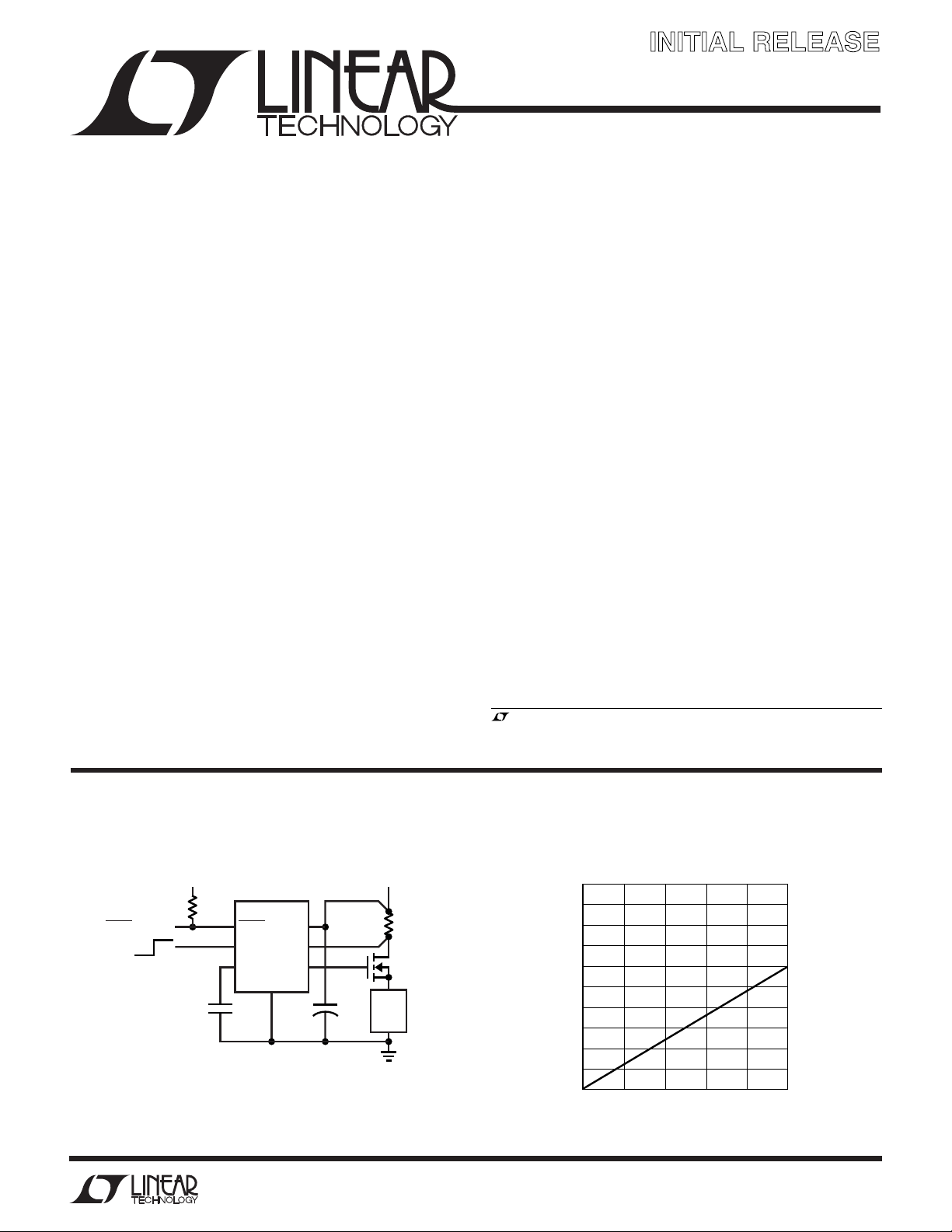
The LT®1910 is a high side gate driver allowing the use of
low cost N-channel power MOSFETs for high side switching applications. It contains a completely self-contained
charge pump to fully enhance an N-channel MOSFET
switch with no external components.
When the internal drain comparator senses that the switch
current has exceeded the preset level, the switch is turned
off and a fault flag is asserted. The switch remains off for
a period of time set by an external timing capacitor and
then automatically attempts to restart. If the fault still
exists, this cycle repeats until the fault is removed, thus
protecting the MOSFET. The fault flag becomes inactive
once the switch restarts successfully.
The LT1910 has been specifically designed for harsh
operating environments such as industrial, avionics and
automotive applications where poor supply regulation
and/or transients may be present. The device will not
sustain damage from supply transients of –15V to 60V.
The LT1910 is available in the SO-8 package.
, LTC and LT are registered trademarks of Linear Technology Corporation.
TYPICAL APPLICATIO
Fault Protected High Side Switch
5.1k
FAULT OUTPUT
OFF ON
U
Switch Drop vs Load Current
24V5V
LT1910
+
FAULT
IN
TIMER
0.1µF
V
SENSE
GATE
GND
+
10µF
50V
Information furnished by Linear Technology Corporation is believed to be accurate and reliable.
However, no responsibility is assumed for its use. Linear Technology Corporation makes no representation that the interconnection of its circuits as described herein will not infringe on existing patent rights.
0.01Ω
IRFZ34
LOAD
1910 TA01
0.50
0.45
0.40
0.35
0.30
0.25
0.20
TOTAL DROP (V)
0.15
0.10
0.05
0
0
1
3
2
LOAD CURRENT (A)
4
5
1910 TA02
1910i
1
LT1910
WW
W
ABSOLUTE MAXIMUM RATINGS
U
U
W
PACKAGE/ORDER INFORMATION
U
(Note 1)
Supply Voltage (Pin 8)............................... –15V to 60V
Input Voltage (Pin 4) .................... (GND – 0.3V) to 15V
GATE Voltage (Pin 5) .............................................. 75V
SENSE Voltage (Pin 6)....................................... V+ ±5V
FAULT Voltage (Pin 3) ............................................ 36V
Current (Pins 1, 2, 4, 5, 6, 8) ............................... 40mA
Operating Temperature Range (Note 2) ...–40°C to 85°C
Junction Temperature Range................ –40°C to 125°C
Storage Temperature Range ................. –65°C to 150°C
GND
TIMER
FAULT
IN
T
JMAX
TOP VIEW
1
2
3
4
S8 PACKAGE
8-LEAD PLASTIC SO
= 125°C, θJA = 150°C/W
+
8
V
NC
7
SENSE
6
GATE
5
ORDER PART
NUMBER
LT1910ES8
S8 PART MARKING
1910
Lead Temperature (Soldering, 10 sec).................. 300°C
Consult LTC Marketing for parts specified with wider operating temperature ranges.
ELECTRICAL CHARACTERISTICS
range, otherwise specifications are at TA = 25°C. V+ = 12V to 48V unless otherwise noted.
SYMBOL PARAMETER CONDITIONS MIN TYP MAX UNITS
I
S
∆I
S(ON)
V
INH
V
INL
I
IN
C
IN
V
T(TH)
V
T(CL)
I
T
V
SENSE
I
SENSE
V
– V+Gate Voltage Above Supply V+ = 8V 4 4.5 6 V
GATE
V
F(TH)
V
FOL
t
ON
t
OFF
t
OFF(CL)
Supply Current (OFF State) V+ = 48V, VIN = 0.8V 1.2 1.9 2.5 mA
Delta Supply Current (ON State) VIN = 2V, Measure Increase in I
Input High Voltage ● 2V
Input Low Voltage ● 0.8 V
Input Current VIN = 2V ● 15 30 50 µA
Input Capacitance (Note 3) 5pF
Timer Threshold Voltage VIN = 2V, Adjust V
Timer Clamp Voltage VIN = 0.8V 3.2 3.5 3.8 V
Timer Charge Current VIN = VT = 2V 9 14 20 µA
Drain Sense Threshold Voltage 50 65 80 mV
Temperature Coefficient (Note 3) 0.33 %/°C
Drain Sense Input Current V+ = 48V, V
FAULT Output High Threshold Voltage VIN = 2V, IF = 1mA, Adjust V
FAULT Output Low Threshold Voltage 3.0 3.3 3.6 V
FAULT Output Low Voltage IF = 1mA ● 0.07 0.4 V
Turn-On Time V+ = 24V, V
Turn-Off Time V+ = 24V, V
Current Limit Turn-Off Time V+ = 24V, (V+ – V
The ● denotes specifications that apply over the full operating temperature
S
= 5V ● 55 110 185 µA
V
IN
T
= 65mV 0.5 1.5 µA
SENSE
+
= 12V ● 7 8.5 10 V
V
+
= 24V ● 10 12 14 V
V
V+ = 48V ● 10 12 14 V
T
GATE
GATE
= 32V, C
= 2V, C
SENSE
= 1nF 100 220 400 µs
GATE
= 1nF 25 100 µs
GATE
)→0.1V, C
= 1nF 20 50 µs
GATE
● 2.6 2.9 3.2 V
3.1 3.4 3.7 V
0.8 1.2 mA
Note 1: Absolute Maximum Ratings are those values beyond which the life
of a device may be impaired.
Note 2: The LT1910E is guaranteed to meet performance specifications
from 0°C to 70°C. Specifications over the –40°C to 85°C operating
temperature range are assured by design, characterization and correlation
with statistical process controls.
Note 3: Guaranteed but not tested.
2
1910i
UW
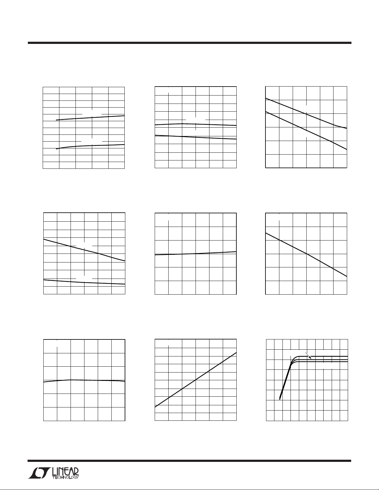
TYPICAL PERFOR A CE CHARACTERISTICS
Supply Current vs Supply Voltage Supply Current vs Temperature Input Voltage vs Temperature
3.6
3.4
3.2
3.0
2.8
2.6
2.4
2.2
2.0
SUPPLY CURRENT (mA)
1.8
1.6
1.4
1.2
10
0
SUPPLY VOLTAGE (V)
20
ON STATE
OFF STATE
30
5.0
V+ = 48V
4.5
4.0
3.5
3.0
2.5
2.0
1.5
SUPPLY CURRENT (mA)
1.0
0.5
0
–25
40
50
1910 G01
–50
ON STATE
OFF STATE
25 50
0
TEMPERATURE (°C)
75
100
1910 G02
2.0
1.8
1.6
1.4
1.2
INPUT VOLTAGE (V)
1.0
0.8
–50
–25
V
V
02550
TEMPERATURE (°C)
LT1910
INH
INL
75 100
1910 G03
Input Current vs Temperature
200
180
160
140
120
100
80
60
INPUT CURRENT (µA)
40
20
0
–50
–25
VIN = 5V
VIN = 2V
25 50
0
TEMPERATURE (°C)
Timer Charge Current
vs Temperature
20
VIN = VT = 2V
18
16
14
12
TIMER CHARGE CURRENT (µA)
10
8
–50
02550
–25
TEMPERATURE (°C)
75
100
1910 G04
75 100
1910 G07
Timer Threshold Voltage
vs Temperature
3.2
VIN = 2V
3.1
3.0
2.9
2.8
2.7
TIMER THRESHOLD VOLTAGE (V)
2.6
–50
02550
–25
TEMPERATURE (°C)
Drain Sense Threshold Voltage
vs Temperature
90
V+ = 24V
85
80
75
70
65
60
55
50
45
DRAIN SENSE THRESHOLD VOLTAGE (mV)
40
–50
–25
25 50
0
TEMPERATURE (°C)
75 100
1910 G05
75
100
1910 G08
Timer Clamp Voltage
vs Temperature
3.8
VIN ≤ 0.8V
3.7
3.6
3.5
3.4
TIMER CLAMP VOLTAGE (V)
3.3
3.2
–50
02550
–25
TEMPERATURE (°C)
MOSFET Gate Voltage Above V
(V
– V+) vs Supply Voltage
GATE
16
) (V)
+
14
– V
GATE
12
(V
+
10
8
6
4
2
0
MOSFET GATE VOLTAGE ABOVE V
0
TA = 25°C
10 20 30 503551525 45
SUPPLY VOLTAGE (V)
75 100
1910 G06
+
TA = 85°C
TA = –40°C
40
LTC1266 • F04
1910i
3
LT1910
UW
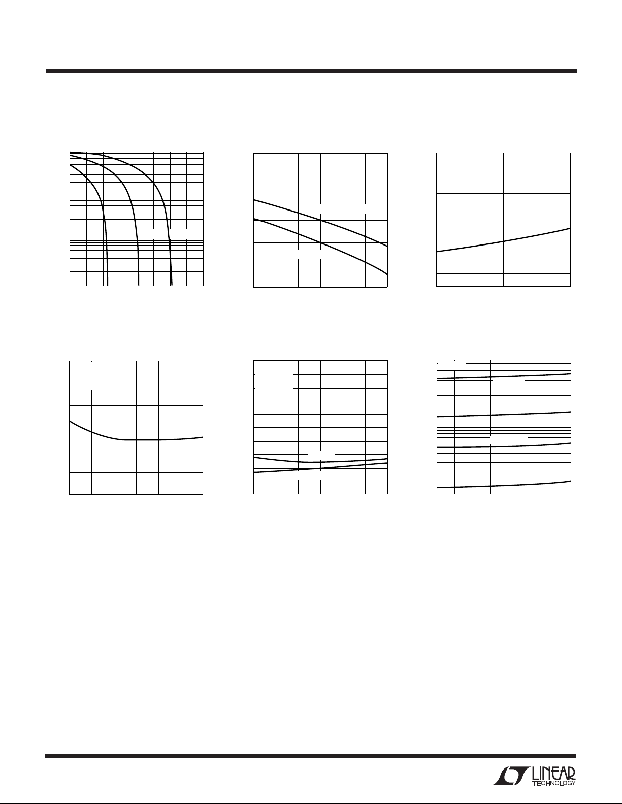
TYPICAL PERFOR A CE CHARACTERISTICS
MOSFET Gate Drive Current
vs V
100
MOSFET GATE DRIVE CURRENT (µA)
GATE
10
1
0.1
024
+
– V
V+ = 8V V+ = 12V V+ ≥ 24V
6 8 10 12 14 16
V
– V+ (V)
GATE
1910 G10
Fault Threshold Voltage
vs Temperature
3.7
VIN = 2V
= 1mA
I
F
3.6
3.5
FAULT HIGH THRESHOLD
3.4
3.3
FAULT LOW THRESHOLD
3.2
FAULT THRESHOLD VOLTAGE (V)
3.1
–50
02550
–25
TEMPERATURE (°C)
Turn-On Time vs Temperature Turn-Off Time vs Temperature
400
V+ = 24V
= 32V
V
GATE
350
300
250
200
TURN-ON TIME (µs)
150
100
–50
C
GATE
= 1nF
02550
–25
TEMPERATURE (°C)
75 100
1910 G13
100
V+ = 24V
90
80
70
60
50
40
30
TURN-OFF TIME (µs)
20
10
0
–50
V
C
GATE
GATE
= 2V
= 1nF
CURRENT LIMIT
–25
0
TEMPERATURE (°C)
NORMAL
25 50
75 100
1910 G11
75
100
1910 G014
Fault Output Low Voltage
vs Temperature
0.20
IF = 1mA
0.18
0.16
0.14
0.12
0.10
0.08
0.06
0.04
FAULT OUTPUT LOW VOLTAGE (V)
0.02
0
–50
–25
25 50
0
TEMPERATURE (°C)
Automatic Restart Period
vs Temperature
1000
V+ = 24V
CT = 3.3µF
CT = 1µF
100
CT = 0.33µF
AUTOMATIC RESTART PERIOD (ms)
10
–50
–30
CT = 0.1µF
–10 10 30 50
TEMPERATURE (°C)
75
100
1910 G012
90
70
1910 G15
4
1910i
 Loading...