

Linear Technology LT1886 Datasheet
FEATURES
LINE VOLTAGE (V
P-P
)
0
HARMONIC DISTORTION (dBc)
–60
–70
–80
–90
–100
1886 TA01a
2 4 6 8 10 12 14 16
VS = 12V
A
V
= 10
f = 200kHz
100Ω LINE
1:2 TRANSFORMER
HD2
HD3
■
700MHz Gain Bandwidth
■
±200mA Minimum I
■
Low Distortion: –72dBc at 1MHz, 4V
■
Stable in AV ≥ 10, Simple Compensation for AV < 10
■
±4.3V Minimum Output Swing, VS = ±6V, RL = 25Ω
■
7mA Supply Current per Amplifier
■
200V/µs Slew Rate
■
Stable with 1000pF Load
■
6nV/√Hz Input Noise Voltage
■
2pA/√Hz Input Noise Current
■
4mV Maximum Input Offset Voltage
■
4µA Maximum Input Bias Current
■
400nA Maximum Input Offset Current
■
±4.5V Minimum Input CMR, VS = ±6V
■
Specified at ±6V, ±2.5V
OUT
, 25Ω, A
P-P
U
APPLICATIO S
V
= 2
LT1886
Dual 700MHz, 200mA
Operational Amplifier
U
DESCRIPTIO
The LT®1886 is a 200mA minimum output current dual op
amp with outstanding distortion performance. The amplifiers are gain-of-ten stable, but can be easily compensated
for lower gains. The LT1886 features balanced, high
impedance inputs with 4µA maximum input bias current,
and 4mV maximum input offset voltage. Single supply
applications are easy to implement and have lower total
noise than current feedback amplifier implementations.
The output drives a 25Ω load to ±4.3V with ±6V supplies.
On ±2.5V supplies the output swings ±1.5V with a 100Ω
load. The amplifier is stable with a 1000pF capacitive
load which makes it useful in buffer and cable driver
applications.
The LT1886 is manufactured on Linear Technology’s
advanced low voltage complementary bipolar process and
is available in a thermally enhanced SO-8 package.
■
DSL Modems
■
xDSL PCI Cards
■
USB Modems
■
Line Drivers
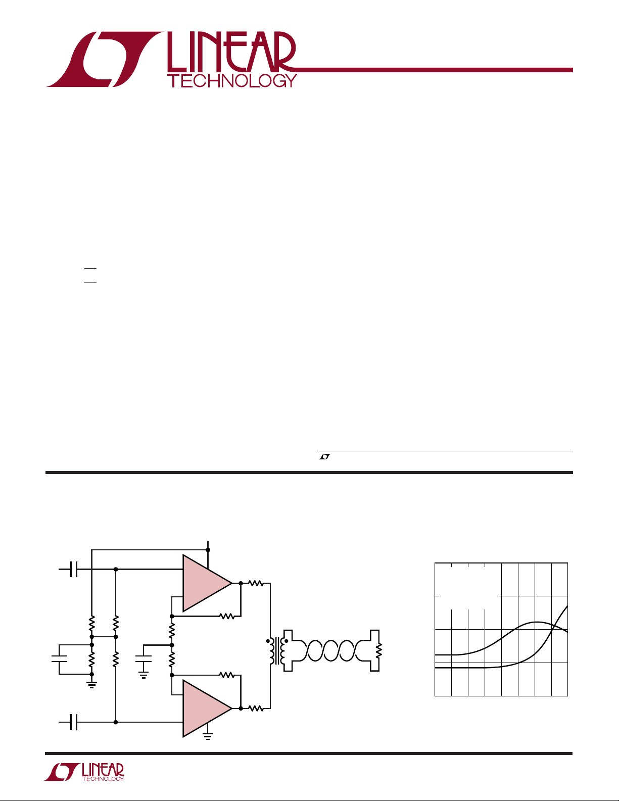
TYPICAL APPLICATIO
0.1µF
+
IN
1µF
0.1µF
–
IN
10k 20k
U
Single 12V Supply ADSL Modem Line Driver
12V
+
1/2 LT1886
–
100Ω
20k10k
1µF
100Ω
–
1/2 LT1886
+
909Ω
909Ω
12.4Ω
12.4Ω
1:2*
1886 TA01
, LTC and LT are registered trademarks of Linear Technology Corporation.
ADSL Modem Line Driver Distortion
100Ω
*COILCRAFT X8390-A
OR EQUIVALENT
1
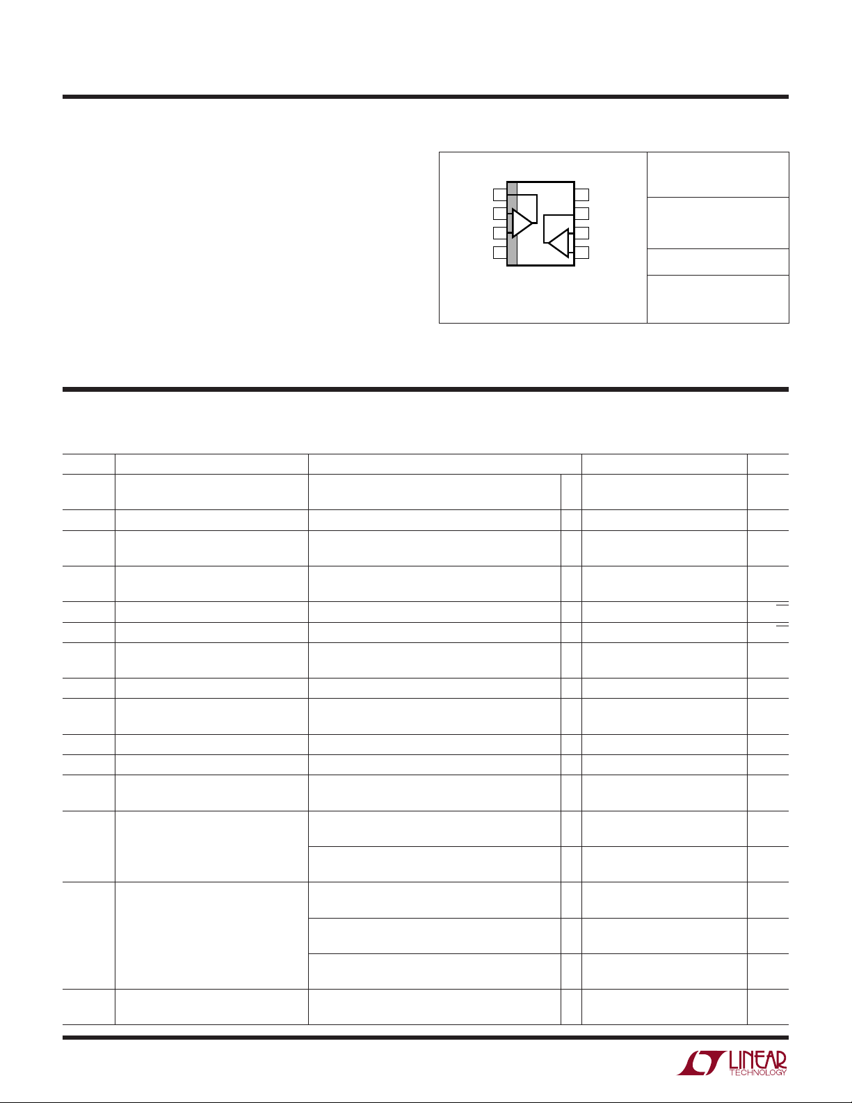
LT1886
1
2
3
4
8
7
6
5
TOP VIEW
V
+
OUT B
–IN B
+IN B
OUT A
–IN A
+IN A
V
–
S8 PACKAGE
8-LEAD PLASTIC SO
B
A
WW
W
ABSOLUTE MAXIMUM RATINGS
U
PACKAGE
/
O
RDER I FOR ATIO
WU
(Note 1)
Total Supply Voltage (V+ to V–) ........................... 13.2V
Input Current (Note 2) ....................................... ±10mA
Input Voltage (Note 2) ............................................ ±V
Maximum Continuous Output Current (Note 3)
S
ORDER PART
NUMBER
LT1886CS8
DC ............................................................... ±100mA
AC ............................................................... ±300mA
Operating Temperature Range (Note 10) –40°C to 85°C
Specified Temperature Range (Note 9).. – 40°C to 85°C
T
= 150°C, θJA = 80°C/W (Note 4)
JMAX
S8 PART MARKING
1886
Maximum Junction Temperature ......................... 150°C
Storage Temperature Range ................ –65°C to 150°C
Consult factory for Industrial and Military grade parts.
Lead Temperature (Soldering, 10 sec)................. 300°C
ELECTRICAL CHARACTERISTICS
erature range, otherwise specifications are at T
SYMBOL PARAMETER CONDITIONS MIN TYP MAX UNITS
V
OS
I
OS
I
B
e
n
i
n
R
IN
C
IN
CMRR Common Mode Rejection Ratio VCM = ±4.5V ● 77 98 dB
PSRR Power Supply Rejection Ratio VS = ±2V to ±6.5V 80 86 dB
A
VOL
V
OUT
I
SC
Input Offset Voltage (Note 5) 1 4 mV
Input Offset Voltage Drift (Note 8) ● 317µV/°C
Input Offset Current 150 400 nA
Input Bias Current 1.5 4 µA
Input Noise Voltage f = 10kHz 6 nV/√Hz
Input Noise Current f = 10kHz 2 pA/√Hz
Input Resistance VCM = ±4.5V 5 10 MΩ
Input Capacitance 2pF
Input Voltage Range (Positive) ● 4.5 5.9 V
Input Voltage Range (Negative)
Minimum Supply Voltage Guaranteed by PSRR ● ±2V
Large-Signal Voltage Gain V
Output Swing RL = 100Ω, 10mV Overdrive 4.85 5 ±V
Short-Circuit Current (Sourcing) (Note 3) 800 mA
Short-Circuit Current (Sinking) 500 mA
= 25°C. VS = ±6V, V
A
Differential 35 kΩ
= ±4V, RL = 100Ω 5.0 12 V/mV
OUT
V
= ±4V, RL = 25Ω 4.5 12 V/mV
OUT
RL = 25Ω, 10mV Overdrive 4.30 4.6 ±V
I
= 200mA, 10mV Overdrive 4.30 4.5 ±V
OUT
The ● denotes specifications which apply over the full operating temp-
= 0V, pulse power tested unless otherwise noted. (Note 9)
CM
● 5mV
● 600 nA
● 6 µA
● –5.2 –4.5 V
● 78 dB
● 4.5 V/mV
● 4.0 V/mV
● 4.70 ±V
● 4.10 ±V
● 4.10 ±V
2
U
LT1886
ELECTRICAL CHARACTERISTICS
erature range, otherwise specifications are at T
= 25°C. VS = ±6V, V
A
The ● denotes specifications which apply over the full operating temp-
= 0V, pulse power tested unless otherwise noted. (Note 9)
CM
SYMBOL PARAMETER CONDITIONS MIN TYP MAX UNITS
SR Slew Rate AV = –10 (Note 6) 133 200 V/µs
● 110 V/µs
Full Power Bandwidth 4V Peak (Note 7) 8 MHz
GBW Gain Bandwidth f = 1MHz 700 MHz
tr, t
Rise Time, Fall Time AV = 10, 10% to 90% of 0.1V, RL = 100Ω 4ns
f
Overshoot AV = 10, 0.1V, RL = 100Ω 1%
Propagation Delay AV = 10, 50% VIN to 50% V
t
S
Settling Time 6V Step, 0.1% 50 ns
Harmonic Distortion HD2, AV = 10, 2V
= 10, 2V
HD3, A
V
, f = 1MHz, RL = 100Ω/25Ω – 75/–63 dBc
P-P
, f = 1MHz, RL = 100Ω/25Ω – 85/–71 dBc
P-P
, 0.1V, RL = 100Ω 2.5 ns
OUT
IMD Intermodulation Distortion AV = 10, f = 0.9MHz, 1MHz, 14dBm, RL = 100Ω/25Ω –81/–80 dBc
R
OUT
I
S
Output Resistance AV = 10, f = 1MHz 0.1 Ω
Channel Separation V
= ±4V, RL = 25Ω 82 92 dB
OUT
● 80 dB
Supply Current Per Amplifier 7 8.25 mA
● 8.50 mA
The ● denotes specifications which apply over the full operating temperature range, otherwise specifications are at TA = 25°C.
V
= ±2.5V, V
S
SYMBOL PARAMETER CONDITIONS MIN TYP MAX UNITS
V
OS
I
OS
I
B
e
n
i
n
R
IN
C
IN
CMRR Common Mode Rejection Ratio VCM = ±1V ● 75 91 dB
A
VOL
V
OUT
= 0V, pulse power tested unless otherwise noted. (Note 9)
CM
Input Offset Voltage (Note 5) 1.5 5 mV
● 6mV
Input Offset Voltage Drift (Note 8) ● 517µV/°C
Input Offset Current 100 350 nA
● 550 nA
Input Bias Current 1.2 3.5 µA
● 5.5 µA
Input Noise Voltage f = 10kHz 6 nV/√Hz
Input Noise Current f = 10kHz 2 pA/√Hz
Input Resistance VCM = ±1V 10 20 MΩ
Differential 50 kΩ
Input Capacitance 2pF
Input Voltage Range (Positive) ● 1 2.4 V
Input Voltage Range (Negative)
Large-Signal Voltage Gain V
= ±1V, RL = 100Ω 5.0 10 V/mV
OUT
V
= ±1V, RL = 25Ω 4.5 10 V/mV
OUT
● –1.7 –1 V
● 4.5 V/mV
● 4.0 V/mV
Output Swing RL = 100Ω, 10mV Overdrive 1.50 1.65 ±V
● 1.40 ±V
RL = 25Ω, 10mV Overdrive 1.35 1.50 ±V
● 1.25 ±V
I
= 200mA, 10mV Overdrive 0.87 1 ±V
OUT
● 0.80 ±V
3
LT1886
ELECTRICAL CHARACTERISTICS
erature range, otherwise specifications are at T
= 25°C. VS = ±2.5V, V
A
The ● denotes specifications which apply over the full operating temp-
= 0V, pulse power tested unless otherwise noted. (Note 9)
CM
SYMBOL PARAMETER CONDITIONS MIN TYP MAX UNITS
I
SC
Short-Circuit Current (Sourcing) (Note 3) 600 mA
Short-Circuit Current (Sinking) 400 mA
SR Slew Rate AV = –10 (Note 6) 66 100 V/µs
● 60 V/µs
Full Power Bandwidth 1V Peak (Note 7) 16 MHz
GBW Gain Bandwidth f = 1MHz 530 MHz
tr, t
Rise Time, Fall Time AV = 10, 10% to 90% of 0.1V, RL = 100Ω 7ns
f
Overshoot AV = 10, 0.1V, RL = 100Ω 5%
Propagation Delay AV = 10, 50% VIN to 50% V
Harmonic Distortion HD2, AV = 10, 2V
= 10, 2V
HD3, A
V
, f = 1MHz, RL = 100Ω/25Ω – 75/–64 dBc
P-P
, f = 1MHz, RL = 100Ω/25Ω – 80/–66 dBc
P-P
, 0.1V, RL = 100Ω 5ns
OUT
IMD Intermodulation Distortion AV = 10, f = 0.9MHz, 1MHz, 5dBm, RL = 100Ω/25Ω – 77/–85 dBc
R
OUT
I
S
Note 1: Absolute Maximum Ratings are those values beyond which the life
of a device may be impaired.
Note 2: The inputs are protected by back-to-back diodes. If the differential
input voltage exceeds 0.7V, the input current should be limited to less than
10mA.
Note 3: A heat sink may be required to keep the junction temperature
below absolute maximum.
Note 4: Thermal resistance varies depending upon the amount of PC board
metal attached to the device. θ
covered with 2 oz copper on both sides.
Note 5: Input offset voltage is exclusive of warm-up drift.
Output Resistance AV = 10, f = 1MHz 0.2 Ω
Channel Separation V
= ±1V, RL = 25Ω 82 92 dB
OUT
● 80 dB
Supply Current Per Amplifier 5 5.75 mA
● 6.25 mA
Note 6: Slew rate is measured between ±2V on a ±4V output with ±6V
supplies, and between ±1V on a ±1.5V output with ±2.5V supplies.
Note 7: Full power bandwidth is calculated from the slew rate:
FPBW = SR/2πV
.
P
Note 8: This parameter is not 100% tested.
Note 9: The LT1886C is guaranteed to meet specified performance from 0°C
to 70°C. The LT1886C is designed, characterized and expected to meet
specified performance from –40°C to 85°C but is not tested or QA sampled
is specified for a 2500mm2 test board
JA
at these temperatures. For guaranteed I-grade parts, consult the factory.
Note 10: The LT1886C is guaranteed functional over the operating temperature
range of –40°C to 85°C.
UW
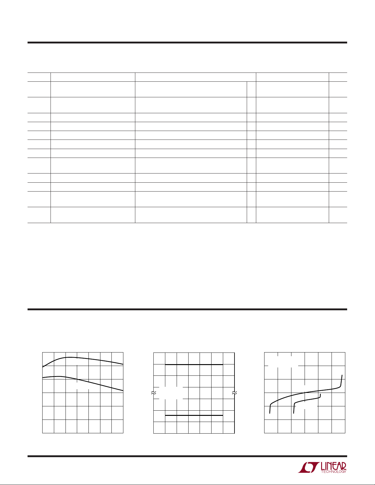
TYPICAL PERFOR A CE CHARACTERISTICS
Input Common Mode Range vs
Supply Current vs Temperature
15
VS = ±6V
10
VS = ±2.5V
5
SUPPLY CURRENT (mA)
0
–50 –25 0 25 50 75 100 125
TEMPERATURE (°C)
1886 G01
Supply Voltage
+
V
–0.1
–0.2
–0.3
TA = 25°C
> 1mV
∆V
1.5
1.0
COMMON MODE RANGE (V)
0.5
V
OS
–
0 2 4 6 8 10 12 14
TOTAL SUPPLY VOLTAGE (V)
4
1886 G02
Input Bias Current vs Input
Common Mode Voltage
3.0
TA = 25°C
= (I
+ + IB–)/2
I
B
2.5
2.0
1.5
1.0
INPUT BIAS CURRENT (µA)
0.5
0
B
VS = ±6V
VS = ±2.5V
–6 –2 2–4 0 4 6
INPUT COMMON MODE VOLTAGE (V)
1886 G03
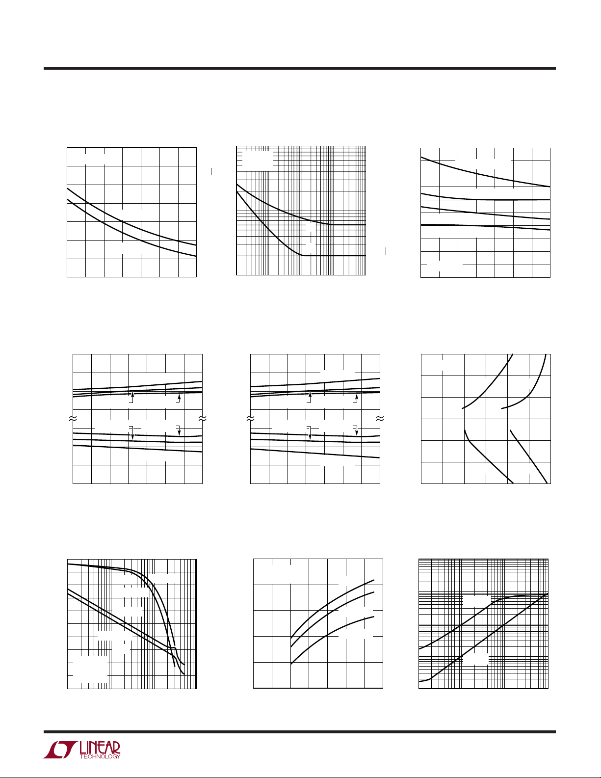
UW
TYPICAL PERFOR A CE CHARACTERISTICS
LT1886
Input Bias Current vs
Temperature Input Noise Spectral Density
3.5
IB = (I
+ + IB–)/2
3.0
2.5
2.0
1.5
1.0
INPUT BIAS CURRENT (µA)
0.5
0
B
VS = ±6V
VS = ±2.5V
–50 –25 0 25 50 75 100 125
TEMPERATURE (°C)
Output Saturation Voltage vs
Temperature, V
+
V
–0.5
–1.0
–1.5
1.5
1.0
0.5
OUTPUT SATURATION VOLTAGE (V)
–
V
IL = 150mA IL = 200mA
IL = 150mA IL = 200mA
–50 –25 0 25 50 75 100 125
= ±6V
S
RL = 100Ω
RL = 100Ω
TEMPERATURE (°C)
1886 G04
1886 G07
100
TA = 25°C
= 101
A
V
10
INPUT VOLTAGE NOISE (nV/√Hz)
1
10
1k 100k100 10k
FREQUENCY (Hz)
Output Saturation Voltage vs
Temperature, V
+
V
–0.5
–1.0
–1.5
1.5
1.0
0.5
OUTPUT SATURATION VOLTAGE (V)
–
V
–50 –25 0 25 50 75 100 125
IL = 150mA IL = 200mA
IL = 150mA IL = 200mA
TEMPERATURE (°C)
Output Short-Circuit Current vs
Temperature
100
10
e
n
i
n
1
1886 G05
= ±2.5V Settling Time vs Output Step
S
RL = 100Ω
RL = 100Ω
1886 G08
1000
900
INPUT CURRENT NOISE (pA/√Hz)
800
700
600
500
400
300
200
100
OUTPUT SHORT-CIRCUIT CURRENT (mA)
0
–50 –25 0 25 50 75 100 125
6
4
2
0
–2
OUTPUT STEP (V)
–4
–6
0204010 30 50 60
SOURCE, VS = ±6V
SOURCE, VS = ±2.5V
SINK, VS = ±6V
SINK, VS = ±2.5V
∆VIN = 0.2V
TEMPERATURE (°C)
VS = ±6V
SETTLING TIME (ns)
10mV 1mV
10mV 1mV
1886 G06
1886 G09
Gain and Phase vs Frequency
80
70
60
50
40
30
GAIN (dB)
20
10
0
–10
–20
1M
TA = 25°C
= –10
A
V
= 100Ω
R
L
PHASE
VS = ±2.5V
VS = ±6V
VS = ±2.5V
GAIN
10M 100M 1G
FREQUENCY (Hz)
VS = ±6V
1886 G10
100
80
60
40
PHASE (DEG)
20
0
–20
–40
–60
–80
–100
Gain Bandwidth vs Supply
Voltage Output Impedance vs Frequency
800
TA = 25°C
= –10
A
V
700
600
500
GAIN BANDWIDTH (MHz)
400
300
2 4 6 8 10 12 14
0
TOTAL SUPPLY VOLTAGE (V)
RL = 1k
RL = 100Ω
RL = 25Ω
1886 G11
100
10
1
0.1
OUTPUT IMPEDANCE (Ω)
0.01
100k 10M 100M
AV = 100
AV = 10
1M
FREQUENCY (Hz)
1886 G12
5
 Loading...