

Linear Technology LT1881, LT1882 Datasheet
FEATURES
Final Electrical Specifications
LT1881/LT1882
Dual and Quad
Rail-to-Rail Output,
Picoamp Input Precision Op Amps
U
DESCRIPTIO
April 2000
■
Offset Voltage: 50µV Maximum (LT1881A)
■
Input Bias Current: 200pA Maximum (LT1881A)
■
Offset Voltage Drift: 0.8µV/°C Maximum
■
Rail-to-Rail Output Swing
■
Supply Range: 2.7V to 36V
■
Operates with Single or Split Supplies
■
Open-Loop Voltage Gain: 1 Million Minimum
■
1mA Maximum Supply Current Per Amplifier
■
Stable at AV = 1, CL = 1000pF
■
Standard Pinouts
U
APPLICATIO S
■
Thermocouple Amplifiers
■
Bridge Transducer Conditioners
■
Instrumentation Amplifiers
■
Battery-Powered Systems
■
Photo Current Amplifiers
The LT®1881 and LT1882 op amps bring high accuracy
input performance to amplifiers with rail-to-rail output
swing. Input bias currents and capacitive load driving
capabilities are superior to the similar LT1884 and LT1885
amplifiers, at the cost of a slight loss in speed. Input
offset voltage is trimmed to less than 50µV and the low
drift maintains this accuracy over the operating temperature range. Input bias currents are an ultralow 200pA
maximum.
The amplifiers work on any total power supply voltage
between 2.7V and 36V (fully specified from 5V to ±15V).
Output voltage swings to within 40mV of the negative
supply and 220mV of the positive supply make these
amplifiers good choices for low voltage single supply
operation.
Capacitive loads up to 1000pF can be driven directly in
unity-gain follower applications.
The dual LT1881 and LT1881A are available with standard
pinouts in S8 and PDIP packages. The quad LT1882 is in
a 14-pin SO package. For a higher speed device with
similar DC specifications, see the LT1884/LT1885.
, LTC and LT are registered trademarks of Linear Technology Corporation.
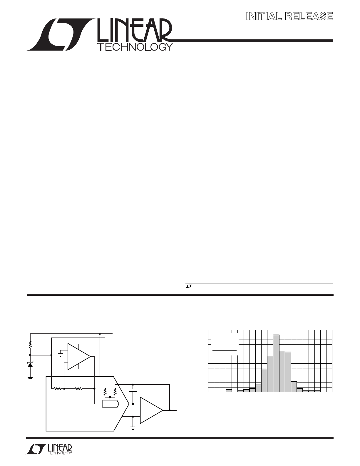
TYPICAL APPLICATIO
16-Bit Voltage Output DAC on ±5V Supply
1.65k
LT1634
4.096V
+
LT1881
–
5V
–5V
R
COM
LTC®1597
REFR1
U
TC VOS Distribution, Industrial Grade
5V
R
OFS
DAC
Information furnished by Linear Technology Corporation is believed to be accurate and reliable.
However, no responsibility is assumed for its use. Linear Technology Corporation makes no representation that the interconnection of its circuits as described herein will not infringe on existing patent rights.
33pF
–
+
LT1881
–5V
5V
V
OUT
–4.096V
TO 4.096V
1881/2 TA01
26
24
VS = ±15V
22
40 N8 (1 LOT)
20
144 S8 (2 LOTS)
18
184 TOTAL PARTS
16
14
12
10
8
PERCENT OF UNITS (%)
6
4
2
0
1 –0.8 –0.6 –0.4 –0.2 0 0.2 0.4 0.6 0.8–0.9 –0.7 –0.5 –0.3 –0.1 0.1 0.3 0.5 0.7 0.9 1
INPUT OFFSET VOLTAGE DRIFT (µV/°C)
1881/2 TA01a
1
LT1881/LT1882
WW
W
ABSOLUTE AXI U RATI GS
U
(Note 1)
Supply Voltage (V+ to V–) ....................................... 40V
Differential Input Voltage (Note 2) .........................±10V
Input Voltage .................................................... V+ to V
Input Current (Note 2) ........................................ ±10mA
Output Short-Circuit Duration (Note 3)............ Indefinite
UUW
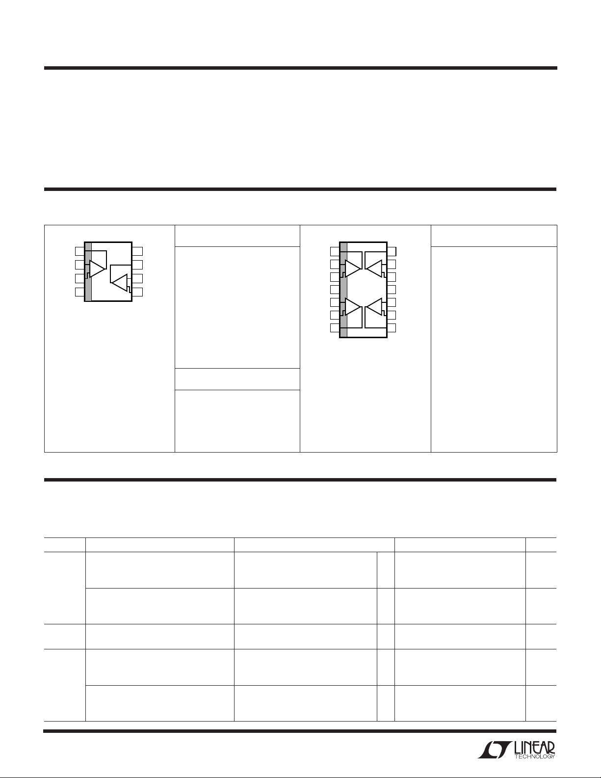
PACKAGE/ORDER I FOR ATIO
TOP VIEW
OUT A
1
–IN A
2
+IN A
N8 PACKAGE
8-LEAD PDIP
T
T
A
3
–
V
4
= 150°C, θJA = 130°C/W (N8)
JMAX
= 150°C, θJA = 190°C/W (S8)
JMAX
+
V
8
OUT B
7
–IN B
6
B
+IN B
5
S8 PACKAGE
8-LEAD PLASTIC SO
ORDER PART NUMBER
LT1881CN8
LT1881IN8
LT1881CS8
LT1881IS8
LT1881ACN8
LT1881AIN8
LT1881ACS8
LT1881AIS8
S8 PART MARKING
Operating Temperature Range (Note 4) .. –40°C to 85°C
Specified Temperature Range (Note 5)... – 40°C to 85°C
–
Maximum Junction Temperature .......................... 150°C
Storage Temperature Range ................. –65°C to 150°C
Lead Temperature (Soldering, 10 sec).................. 300°C
1
OUT A
2
–IN A
3
+IN A
+
4
V
5
+IN B
6
–IN B
7
OUT B
14-LEAD PLASTIC SO
T
JMAX
TOP VIEW
14
13
DA
12
11
10
DB
9
8
S PACKAGE
= 150°C, θJA = 150°C/W
OUT D
–IN D
+IN D
–
V
+IN C
–IN C
OUT C
ORDER PART NUMBER
LT1882CS
LT1882IS
1881
1881I
1881A
1881AI
Consult factory for Military grade parts.
ELECTRICAL CHARACTERISTICS
The ● denotes the specifications which apply over the full operating temperature range, otherwise specifications are at TA = 25°C.
Single supply operation VEE = 0, VCC = 5V; VCM = VCC/2 unless otherwise noted. (Note 5)
SYMBOL PARAMETER CONDITIONS MIN TYP MAX UNITS
V
OS
I
OS
Input Offset Voltage (LT1881A) 25 50 µV
< 70°C ● 85 µV
0°C < T
A
–40°C < T
Input Offset Voltage (LT1881/LT1882) 30 80 µV
0°C < T
–40°C < T
Input Offset Voltage Drift 0°C < TA < 70°C ● 0.3 0.8 µV/°C
(Note 6) –40°C < T
Input Offset Current (LT1881A) 100 200 pA
0°C < T
–40°C < T
Input Offset Current (LT1881/LT1882) 150 500 pA
0°C < T
–40°C < T
< 85°C ● 110 µV
A
< 70°C ● 125 µV
A
< 85°C ● 150 µV
A
< 85°C ● 0.3 0.8 µV/°C
A
< 70°C ● 250 pA
A
< 85°C ● 300 pA
A
< 70°C ● 600 pA
A
< 85°C ● 700 pA
A
2
LT1881/LT1882
ELECTRICAL CHARACTERISTICS
The ● denotes the specifications which apply over the full operating temperature range, otherwise specifications are at TA = 25°C.
Single supply operation VEE = 0, VCC = 5V; VCM = VCC/2 unless otherwise noted. (Note 5)
SYMBOL PARAMETER CONDITIONS MIN TYP MAX UNITS
I
B
e
n
i
n
V
CM
CMRR Common Mode Rejection Ratio 1V < VCM < 4V 106 128 dB
PSRR Power Supply Rejection Ratio VEE = 0, VCM = 1.5V; 2.7V < VCC < 32V ● 106 132 dB
A
VOL
V
OL
V
OH
I
S
I
SC
GBW Gain-Bandwidth Product f = 20kHz 0.5 1.0 MHz
t
S
+
SR
–
SR
Input Bias Current (LT1881A) 100 200 pA
< 70°C ● 250 pA
0°C < T
A
–40°C < T
< 85°C ● 300 pA
A
Input Bias Current (LT1881/LT1882) 150 500 pA
< 70°C ● 600 pA
0°C < T
A
–40°C < T
Input Noise Voltage 0.1Hz to 10Hz 0.5 µV
< 85°C ● 700 pA
A
P-P
Input Noise Voltage Density f = 1kHz 14 nV/√Hz
Input Noise Current Density f = 1kHz 0.03 pA/√Hz
Input Voltage Range VEE + 1.0 VCC – 1.0 V
1.2V < V
● V
< 3.8V ● 104 dB
CM
+ 1.2 VCC – 1.2 V
EE
Minimum Operating Supply Voltage ● 2.4 2.7 V
Large-Signal Voltage Gain RL = 10k; 1V < V
RL = 2k; 1V < V
RL = 1k; 1V < V
< 4V 500 1600 V/mV
OUT
< 4V 300 800 V/mV
OUT
< 4V 250 400 V/mV
OUT
● 350 V/mV
● 250 V/mV
● 200 V/mV
Output Voltage Swing Low No Load ● 20 40 mV
I
= 100µA ● 25 50 mV
SINK
= 1mA ● 70 150 mV
I
SINK
= 5mA ● 270 600 mV
I
SINK
Output Voltage Swing High No Load ● 120 220 mV
(Referred to V
)I
CC
= 100µA ● 130 230 mV
SOURCE
I
= 1mA ● 180 300 mV
SOURCE
= 5mA ● 360 600 mV
I
SOURCE
Supply Current Per Amplifier VCC = 3V 0.45 0.65 0.85 mA
● 1.2 mA
VCC = 5V 0.5 0.65 0.9 mA
● 1.4 mA
VCC = 12V 0.5 0.70 1.0 mA
● 1.5 mA
Short-Circuit Current V
Settling Time 0.01%, V
Short to GND ● 15 30 mA
OUT
Short to V
V
OUT
= –1, RL = 2k
A
V
CC
= 1.5V to 3.5V, 30 µs
OUT
● 15 30 mA
Slew Rate Positive AV = –1 0.15 0.35 V/µs
● 0.12 V/µs
Slew Rate Negative AV = –1 0.11 0.18 V/µs
● 0.08 V/µs
3
LT1881/LT1882
ELECTRICAL CHARACTERISTICS
The ● denotes the specifications which apply over the full operating temperature range, otherwise specifications are at TA = 25°C.
Single supply operation VEE = 0, VCC = 5V; VCM = VCC/2 unless otherwise noted. (Note 5)
SYMBOL PARAMETER CONDITIONS MIN TYP MAX UNITS
∆V
OS
∆IB+ Noninverting Bias Current Match (Notes 7, 8) 200 300 pA
∆CMRR Common Mode Rejection Match (Notes 7, 9) ● 102 125 dB
∆PSRR Power Supply Rejection Match VEE = 0V, VCM = 1.5V, 2.7V < VCC < 32V, ● 104 126 dB
Offset Voltage Match (LT1881A) (Note 7) 30 70 µV
0°C < T
< 70°C ● 125 µV
A
–40°C < T
< 85°C ● 160 µV
A
Offset Voltage Match (LT1881/LT1882) (Note 7) 35 125 µV
< 70°C ● 175 µV
0°C < T
A
–40°C < T
< 85°C ● 235 µV
A
Offset Voltage Match Drift (Notes 6, 7) ● 0.4 1.2 µV/°C
(LT1881A) 0°C < T
< 70°C ● 400 pA
A
–40°C < T
< 85°C ● 500 pA
A
Noninverting Bias Current Match (Notes 7, 8) 250 700 pA
(LT1881/LT1882) 0°C < T
< 70°C ● 900 pA
A
–40°C < T
< 85°C ● 1000 pA
A
(Notes 7, 9)
The ● denotes the specifications which apply over the full operating temperature range, otherwise specifications are at TA = 25°C.
Split supply operation VS = ±15V, VCM = 0V unless otherwise noted. (Note 5)
SYMBOL PARAMETER CONDITIONS MIN TYP MAX UNITS
V
OS
I
OS
I
B
e
n
i
n
V
CM
Input Offset Voltage (LT1881A) 25 50 µV
< 70°C ● 85 µV
0°C < T
A
–40°C < T
< 85°C ● 110 µV
A
Input Offset Voltage (LT1881/LT1882) 30 80 µV
0°C < T
< 70°C ● 125 µV
A
–40°C < T
< 85°C ● 150 µV
A
Input Offset Voltage Drift 0°C < TA < 70°C ● 0.3 0.8 µV/°C
(Note 6) –40°C < T
< 85°C ● 0.3 0.8 µV/°C
A
Input Offset Current (LT1881A) 150 200 pA
< 70°C ● 250 pA
0°C < T
A
–40°C < T
< 85°C ● 300 pA
A
Input Offset Current (LT1881/LT1882) 150 500 pA
< 70°C ● 600 pA
0°C < T
A
–40°C < T
< 85°C ● 700 pA
A
Input Bias Current (LT1881A) 150 200 pA
0°C < T
< 70°C ● 250 pA
A
–40°C < T
< 85°C ● 300 pA
A
Input Bias Current (LT1881/LT1882) 150 500 pA
< 70°C ● 600 pA
0°C < T
A
–40°C < T
Input Noise Voltage 0.1Hz to 10Hz 0.5 µV
< 85°C ● 700 pA
A
P-P
Input Noise Voltage Density f = 1kHz 14 nV/√Hz
Input Noise Current Density f = 1kHz 0.03 pA/√Hz
Input Voltage Range VEE + 1.0 VCC – 1.0 V
● V
+ 1.2 VCC – 1.2 V
EE
4
 Loading...