

FEATURES
LT1880
SOT-23, Rail-to-Rail Output,
Picoamp Input Current
Precision Op Amp
U
DESCRIPTIO
■
Offset Voltage: 150µV Max
■
Input Bias Current: 900pA Max
■
Offset Voltage Drift: 1.2µV/°C Max
■
Rail-to-Rail Output Swing
■
Operates with Single or Split Supplies
■
Open-Loop Voltage Gain: 1 Million Min
■
1.2mA Supply Current
■
Slew Rate: 0.4V/µs
■
Gain Bandwidth: 1.1MHz
■
Low Noise: 13nV/√Hz at 1kHz
■
Low Profile (1mm) ThinSOT
TM
Package
U
APPLICATIO S
■
Thermocouple Amplifiers
■
Bridge Transducer Conditioners
■
Instrumentation Amplifiers
■
Battery-Powered Systems
■
Photocurrent Amplifiers
U
TYPICAL APPLICATIO
The LT®1880 op amp brings high accuracy input performance and rail-to-rail output swing to the SOT-23 package. Input offset voltage is trimmed to less than 150µV and
the low drift maintains this accuracy over the operating
temperature range. Input bias current is an ultra low
900pA maximum.
The amplifier works on any total power supply voltage
between 2.7V and 36V (fully specified from 5V to ±15V).
Output voltage swings to within 55mV of the negative
supply and 250mV of the positive supply, which makes the
amplifier a good choice for low voltage single supply
operation.
Slew rates of 0.4V/µs with a supply current of 1.2mA give
superior response and settling time performance in a low
power precision amplifier.
The LT1880 is available in a 5-lead SOT-23 package.
, LTC and LT are registered trademarks of Linear Technology Corporation.
ThinSOT is a trademark of Linear Technology Corporation.
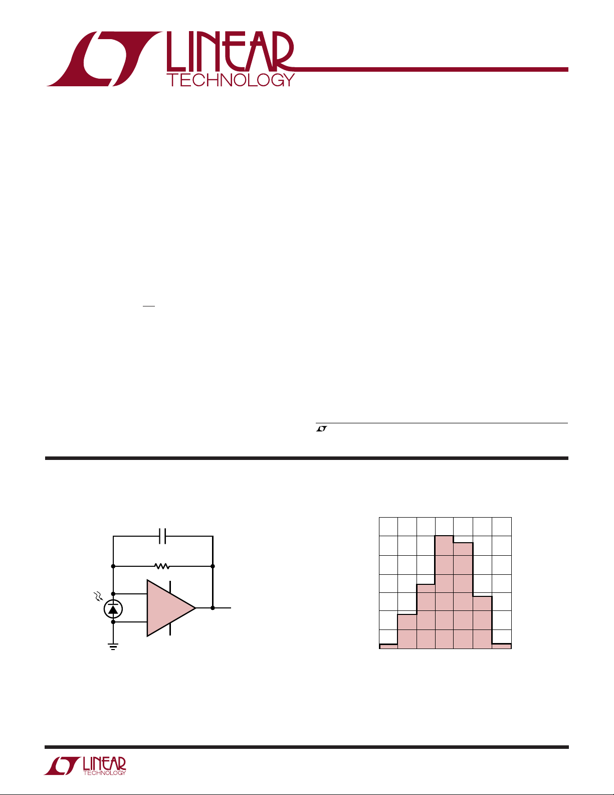
Precision Photodiode Amplifier
C1
39pF
R1
100k, 1%
+
V
V
λ
S1
320µV OUTPUT OFFSET, WORST CASE OVER 0°C TO 70°C
60kHz BANDWIDTH
5.8µs RISE TIME, 10% TO 90%, 100mV OUTPUT STEP
52µV
OUTPUT NOISE, MEASURED ON A 100kHz BW
RMS
V
= ±1.5V TO ±18V
S
S1: SIEMENS INFINEON BPW21 PHOTODIODE (~580pF)
–
+
S
LT1880
V
S
–
V
OUT
OUT
= 0.1V/µA
1880 TA01
Distribution of Input Offset Voltage
35
30
25
20
15
10
PERCENT OF UNITS (%)
5
0
–140
–100 –60
INPUT OFFSET VOLTAGE (µV)
20 100 140
–20 60
1880 TA01b
1
LT1880
WW
W
ABSOLUTE AXI U RATI GS
U
UUW
PACKAGE/ORDER I FOR ATIO
(Note 1)
Supply Voltage (V+ to V–) ....................................... 40V
Differential Input Voltage (Note 2) ......................... ±10V
Input Voltage .................................................... V+ to V
Input Current (Note 2) ........................................ ±10mA
Output Short-Circuit Duration (Note 3)............ Indefinite
Operating Temperature Range (Note 4) .. –40°C to 85°C
Specified Temperature Range (Note 5)... – 40°C to 85°C
Maximum Junction Temperature .......................... 150°C
Storage Temperature Range ................. –65°C to 150°C
Lead Temperature (Soldering, 10 sec).................. 300°C
ELECTRICAL CHARACTERISTICS
The ● denotes the specifications which apply over the full operating
–
OUT 1
Consult LTC Marketing for parts specified with wider operating temperature ranges.
TOP VIEW
–
V
2
+IN 3
S5 PACKAGE
5-LEAD PLASTIC SOT-23
T
= 150°C, θJA = 250°C/W
JMAX
5 V
4 –IN
+
ORDER PART
NUMBER
LT1880CS5
LT1880IS5
S5 PART
MARKING
LTUM
LTVW
temperature range, otherwise specifications are at TA = 25°C. VS = 5V, 0V; VCM = 2.5V unless otherwise noted. (Note 5)
SYMBOL PARAMETER CONDITIONS MIN TYP MAX UNITS
V
OS
I
OS
I
B
e
n
i
n
R
IN
C
IN
V
CM
CMRR Common Mode Rejection Ratio 1V < VCM < 3.8V ● 116 135 dB
PSRR Power Supply Rejection Ratio V– = 0V, VCM = 1.5V; 2.7V < V+ < 32V ● 110 135 dB
A
VOL
V
OL
Input Offset Voltage 40 150 µV
0°C < T
< 70°C ● 200 µV
A
–40°C < T
Input Offset Voltage Drift 0°C < TA < 70°C ● 0.3 1.2 µV/°C
(Note 6) –40°C < T
Input Offset Current 150 900 pA
0°C < T
–40°C < T
Input Bias Current 150 900 pA
0°C < T
–40°C < T
Input Noise Voltage 0.1Hz to 10Hz 0.5 µV
Input Noise Voltage Density f = 1kHz 13 nV/√Hz
Input Noise Current Density f = 1kHz 0.07 pA/√Hz
Input Resistance Differential 380 MΩ
Common Mode, V
Input Capacitance 3.7 pF
Input Voltage Range ● (V– + 1.0) (V+ – 1.2) V
Minimum Operating Supply Voltage ● 2.4 2.7 V
Large Signal Voltage Gain RL = 10k; 1V < V
R
L
R
L
Output Voltage Swing Low No Load ● 20 55 mV
I
SINK
I
SINK
< 85°C ● 250 µV
A
< 85°C ● 0.3 1.2 µV/°C
A
< 70°C ● 1200 pA
A
< 85°C ● 1400 pA
A
< 70°C ● 1200 pA
A
< 85°C ● 1500 pA
A
= 1V to 3.8V 210 GΩ
CM
< 4V 500 1600 V/mV
OUT
= 2k; 1V < V
= 1k; 1V < V
= 100µA ● 35 65 mV
= 1mA ● 130 200 mV
< 4V 400 800 V/mV
OUT
< 4V 300 400 V/mV
OUT
● 400 V/mV
● 300 V/mV
● 250 V/mV
P-P
2

LT1880
ELECTRICAL CHARACTERISTICS
The ● denotes the specifications which apply over the full operating
temperature range, otherwise specifications are at TA = 25°C. VS = 5V, 0V; VCM = 2.5V unless otherwise noted. (Note 5)
SYMBOL PARAMETER CONDITIONS MIN TYP MAX UNITS
V
OH
I
S
I
SC
GBW Gain-Bandwidth Product f = 20kHz 0.8 1.1 MHz
t
S
FPBW Full Power Bandwidth (Note 7) V
THD Total Harmonic Distortion and Noise VO = 2V
+
SR
–
SR
Output Voltage Swing High V+ = 5V; No Load ● 130 250 mV
(Referred to V
+
)V
+
= 5V; I
+
= 5V; I
V
= 100µA ● 150 270 mV
SOURCE
= 1mA ● 220 380 mV
SOURCE
Supply Current per Amplifier V+ = 3V 1.2 1.8 mA
● 2.2 mA
V+ = 5V 1.2 1.9 mA
● 2.3 mA
V+ = 12V 1.35 2 mA
● 2.4 mA
Short-Circuit Current V
Settling Time 0.01%, V
Short to GND ● 10 18 mA
OUT
Short to V
V
OUT
= –1, RL = 2k
A
V
= 4V
OUT
= 2V
V
O
+
= 1.5V to 3.5V 10 µs
OUT
P-P
, AV = –1, f = 1kHz, Rf = 1k, BW = 22kHz 0.002 %
P-P
, AV = 1, f = 1kHz, RL = 10k, BW = 22kHz 0.0008 %
P-P
● 10 20 mA
32 kHz
Slew Rate Positive AV = –1 0.25 0.4 V/µs
● 0.2 V/µs
Slew Rate Negative AV = –1 0.25 0.55 V/µs
● 0.25 V/µs
The ● denotes the specifications which apply over the full operating temperature range, otherwise specifications are at TA = 25°C.
VS= ±15V, VCM = 0V unless otherwise noted. (Note 5)
SYMBOL PARAMETER CONDITIONS MIN TYP MAX UNITS
V
OS
I
OS
I
B
e
n
i
n
R
IN
C
IN
V
CM
CMRR Common Mode Rejection Ratio –13.5V < VCM < 13.5V ● 118 135 dB
+PSRR Positive Power Supply Rejection Ratio V– = –15V, VCM = 0V; 1.5V < V+ < 18V ● 110 135 dB
–PSRR Negative Power Supply Rejection Ratio V+ = 15V, VCM = 0V; –1.5V < V– < –18V ● 110 135 dB
Input Offset Voltage 40 150 µV
0°C < T
< 70°C ● 200 µV
A
–40°C < T
< 85°C ● 250 µV
A
Input Offset Voltage Drift 0°C < TA < 70°C ● 0.3 1.2 µV/°C
(Note 6) –40°C < T
< 85°C ● 0.3 1.2 µV/°C
A
Input Offset Current 150 900 pA
< 70°C ● 1200 pA
0°C < T
A
–40°C < T
< 85°C ● 1400 pA
A
Input Bias Current 150 900 pA
< 70°C ● 1200 pA
0°C < T
A
–40°C < T
Input Noise Voltage 0.1Hz to 10Hz 0.5 µV
< 85°C ● 1500 pA
A
P-P
Input Noise Voltage Density f = 1kHz 13 nV/√Hz
Input Noise Current Density f = 1kHz 0.07 pA/√Hz
Input Resistance Differential 380 MΩ
Common Mode, V
= –13.5V to 13.5V 190 GΩ
CM
Input Capacitance 3.7 pF
Input Voltage Range ● –13.5 13.5 V
Minimum Operating Supply Voltage ● ±1.2 ±1.35 V
3

LT1880
ELECTRICAL CHARACTERISTICS
The ● denotes the specifications which apply over the full operating
temperature range, otherwise specifications are at TA = 25°C. VS = ±15V; VCM = 0V unless otherwise noted. (Note 5)
SYMBOL PARAMETER CONDITIONS MIN TYP MAX UNITS
A
VOL
V
OL
V
OH
I
S
I
SC
FPBW Full Power Bandwidth (Note 7) V
GBW Gain Bandwidth Product f = 20kHz 0.8 1.1 MHz
THD Total Harmonic Distortion and Noise VO = 25V
+
SR
–
SR
Note 1: Absolute Maximum Ratings are those values beyond which the life
of a device may be impaired.
Note 2: The inputs are protected by back-to-back diodes. If the differential
input voltage exceeds 10V, see Application Information, the input current
should be limited to less than 10mA.
Note 3: A heat sink may be required to keep the junction temperature
below absolute maximum ratings.
Note 4: The LT1880C and LT1880I are guaranteed functional over the
operating temperature range of –40°C to 85°C.
Large Signal Voltage Gain RL = 10k; –13.5V < V
R
= 2k; –13.5V < V
L
< 13.5V 1000 1600 V/mV
OUT
< 13.5V 500 1000 V/mV
OUT
● 700 V/mV
● 300 V/mV
Output Voltage Swing Low No Load ● 25 65 mV
(Referred to V
)I
EE
= 100µA ● 35 75 mV
SINK
= 1mA ● 130 200 mV
I
SINK
Output Voltage Swing High No Load ● 185 350 mV
(Referred to V
)I
CC
= 100µA ● 195 370 mV
SOURCE
= 1mA ● 270 450 mV
I
SOURCE
Supply Current per Amplifier 1.5 2.3 mA
● 1.8 2.8 mA
Short-Circuit Current V
OUT
V
OUT
OUT
V
O
= 25V
Short to V
Short to V
= 14V
–
+
P-P
, AV = –1, f = 100kHz, Rf = 10k, BW = 22kHz 0.00029 %
P-P
, AV = 1, f = 100kHz, RL = 10k, BW = 22kHz 0.00029 %
P-P
10 25 mA
● 10 25 mA
10 20 mA
● 10 20 mA
9kHz
Slew Rate Positive AV = –1 0.25 0.4 V/µs
● 0.2 V/µs
Slew Rate Negative AV = –1 0.25 0.55 V/µs
● 0.2 V/µs
Note 5: The LT1880C is guaranteed to meet specified performance from
0°C to 70°C and is designed, characterized and expected to meet specified
performance from –40°C to 85°C but is not tested or QA sampled at these
temperatures. The LT1880I is guaranteed to meet specified performance
from –40°C to 85°C.
Note 6: This parameter is not 100% tested.
Note 7: Full power bandwidth is calculated from the slew rate.
FPBW = SR/(2πVP)
4

UW
TYPICAL PERFOR A CE CHARACTERISTICS
LT1880
Input Offset Voltage vs
Temperature
200
TEMPCO: –55°C TO 125°C
10 REPRESENTATIVE UNITS
150
100
50
0
–50
–100
INPUT OFFSET VOLTAGE (µV)
–150
–200
–55 –35
–15 105
255
TEMPERATURE (°C)
Input Bias Current vs Common
Mode Near V
1000
500
0
–500
INPUT BIAS CURRENT (pA)
–1000
–14.6
EE
–
I
B
+
I
B
–14.2
COMMON MODE VOLTAGE (V)
–13.8
856545
VS = ±15V
TA = –40°C
= 25°C
T
A
= 85°C
T
A
–13.4
1880 G01
1880 G02B
125
–13.0
Input Bias Current vs Common
Mode Voltage
1000
800
600
400
200
–200
–400
INPUT BIAS CURRENT (pA)
–600
–800
–1000
0
–15
TA = 25°C
T
= –40°C
A
T
= 85°C
A
VS = ±15V
–10
–5
COMMON MODE VOLTAGE (V)
–
I
B
+
I
B
05
Input Bias Current vs
Temperature
200
VS = ±15V
150
100
50
0
–50
–100
–150
INPUT BIAS CURRENT (pA)
–200
–250
–300
–50
–25
TEMPERATURE (°C)
0
–
I
B
+
I
B
25 50
Input Bias Current vs Common
Mode Near V
1000
500
0
–500
INPUT BIAS CURRENT (pA)
–1000
15
10
1880 G02
13.0
CC
–
I
B
+
I
B
13.4
COMMON MODE VOLTAGE (V)
13.8
VS = ±15V
TA = –45°C
T
A
T
A
14.2
= 25°C
= 85°C
14.6
1880 G02A
Output Voltage Swing
vs Load Current
TA = 85°C
TA = 25°C
2–8 –4 0 4 86
TA = –40°C
10
1880 G04
)
–0.5
+
–1.0
SWING (V
–1.5
OUTPUT VOLTAGE
1.5
1.0
0.5
–10
TA = 25°C
TA = 85°C
TA = –40°C
–6
OUTPUT CURRENT (mA)
–2
)
–
SWING (V
OUTPUT VOLTAGE
100
75
1880 G03
Warm Up Drift
6
TA = 25°C
5
4
3
2
OFFSET VOLTAGE CHANGE (µV)
1
0
0
VS = ±15V
VS = ±2.5V
1234
TIME AFTER POWER ON (MIN)
1880 G05
en, in vs Frequency 0.1 to 10Hz Noise
1000
CURRENT NOISE
100
VOLTAGE NOISE
10
CURRENT NOISE DENSITY (fA/√Hz)
VOLTAGE NOISE DENSITY (nV/√Hz)
5
1
1
10 100 1k
FREQUENCY (Hz)
VS = ±15V
= 25°C
T
A
1880 G08
NOISE VOLTAGE (0.2µV/DIV)
VS = ±15V
= 25°C
T
A
2
0
4
TIME (SEC)
6
8
10
1880 G09a
5

LT1880
UW
TYPICAL PERFOR A CE CHARACTERISTICS
0.01 to 1Hz Noise
NOISE VOLTAGE (0.2µV/DIV)
20
0
40
TIME (SEC)
60
CMRR vs Frequency
160
140
120
100
80
60
40
20
POWER SUPPLY REJECTION RATIO (dB)
0
1
100 1k 10k 100k 1M
10
FREQUENCY (Hz)
VS = ±15V
= 25°C
T
A
80
1880 G09b
VS = ±15V
1880 G12
100
Gain vs Frequency
140
120
100
80
60
40
GAIN (dB)
20
0
–20
–40
0.1
10
1 10M
100 1k 10k
FREQUENCY (Hz)
Gain and Phase vs Frequency
70
60
50
40
30
20
10
VOLTAGE GAIN (dB)
0
–10
–20
–30
10k
PHASE SHIFT
GAIN
100k 1M 10M
FREQUENCY (Hz)
VS = ±15V
100k
VS = ±15V
1880 G13
1M
1880 G10
100
80
60
40
20
0
–20
–40
–60
–80
–100
PSRR vs Frequency
160
140
120
100
80
60
40
20
POWER SUPPLY REJECTION RATIO (dB)
0
0.1 1
10
Settling Time vs Output Step
10
VS = ±15V
8
= –1
A
V
PHASE SHIFT (DEG)
6
4
2
0
–2
OUTPUT STEP (V)
–4
–6
–8
–10
0
515
0.1%
10
SETTLING TIME (µs)
VS = ±15V
–PSRR
+PSRR
100 1k 10k 100k 1M
FREQUENCY (Hz)
0.1%
0.01%
0.01%
20
30
25
35
1880 G11
40
1880 G14
Settling Time vs Output Step
10
VS = ±15V
8
= 1
A
V
6
4
2
0
–2
OUTPUT STEP (V)
–4
–6
–8
–10
0
0.1%
0.1%
10
515
SETTLING TIME (µs)
6
20
0.01%
0.01%
Slew Rate, Gain-Bandwidth
Product and Phase Margin vs
Temperature
0.5
VS = ±15V
0.4
SLEW RATE (V/µs)
0.3
1.14
1.12
PRODUCT (MHz)
GAIN BANDWIDTH
1.10
35
30
25
1880 G15
–50
GBW
–25
0
TEMPERATURE (°C)
SLEW RATE
Φ
M
25 50
PHASE MARGIN (DEG)
68
64
60
100
75
1880 G16
Slew Rate, Gain-Bandwidth
Product and Phase Margin vs
Power Supply
0.5
TA = 25°C
0.4
0.3
1.12
1.11
PRODUCT (MHz) SLEW RATE (V/µs)
GAIN BANDWIDTH
1.10
0
2.5
GBW
SLEW RATE
5
POWER SUPPLY (±V)
Φ
M
7.5 10
12.5
64
60
56
15
1880 G17
PHASE MARGIN (DEG)

UW
TYPICAL PERFOR A CE CHARACTERISTICS
LT1880
Gain vs Frequency
with C
10
0
–10
GAIN (dB)
–20
–30
–40
1k 1M
, AV = –1
LOAD
FREQUENCY (Hz)
0pF
Total Harmonic Distortion + Noise
vs Frequency
10
VS = 5V, 0V
V
= 2.5V
CM
= RG = 1k
R
f
1.0
0.1
= 2V
V
OUT
RL = 10k
P-P
1000pF
500pF
100M10k 100k 10M
1880 G18
Gain vs Frequency
with C
10
0
–10
GAIN (dB)
–20
–30
–40
LOAD
1k 1M
Small Signal Response
V
OUT
(20mV/DIV)
, AV = 1
0pF
FREQUENCY (Hz)
1000pF
500pF
1880 G19
Output Impedance vs Frequency
100
VS = ±15V
10
AV = 100
1.0
0.1
OUTPUT IMPEDANCE (Ω)
100M10k 100k 10M
0.01
0.01 1.0 10 100
AV = 10
AV = 1
0.1
FREQUENCY (MHz)
1880 G17A
Small Signal Response
V
OUT
(20mV/DIV)
0.01
THD + NOISE (%)
0.001
0.0001
10 1k 10k 100k
AV = –1
AV = 1
100
FREQUENCY (Hz)
Small Signal Response
V
OUT
(20mV/DIV)
AV = 1
= 500pF
C
L
TIME (2µs/DIV)
1880 G17B
1880 G22
AV = –1
NO LOAD
Large Signal Response
V
OUT
(5V/DIV)
AV = –1
TIME (2µs/DIV)
TIME (50µs/DIV)
1880 G20
1880 G23
AV = 1
NO LOAD
Large Signal Response
V
OUT
(5V/DIV)
AV = 1
TIME (2µs/DIV)
TIME (50µs/DIV)
1880 G21
1880 G24
7

LT1880
WUUU
APPLICATIO S I FOR ATIO
The LT1880 single op amp features exceptional input
precision with rail-to-rail output swing. Slew rate and
small signal bandwidth are superior to other amplifiers
with comparable input precision. These characteristics
make the LT1880 a convenient choice for precision low
voltage systems and for improved AC performance in
higher voltage precision systems. Obtaining beneficial
advantage of the precision inherent in the amplifier depends upon proper applications circuit design and board
layout.
Preserving Input Precision
Preserving the input voltage accuracy of the LT1880
requires that the applications circuit and PC board layout
do not introduce errors comparable to or greater than the
40µV offset. Temperature differentials across the input
connections can generate thermocouple voltages of 10’s
of microvolts. PC board layouts should keep connections
to the amplifier’s input pins close together and away from
heat dissipating components. Air currents across the
board can also generate temperature differentials.
The extremely low input bias currents, 150pA, allow high
accuracy to be maintained with high impedance sources
and feedback networks. The LT1880’s low input bias
currents are obtained by using a cancellation circuit onchip. This causes the resulting I
BIAS
+
and I
BIAS
–
to be
uncorrelated, as implied by the lOS specification being
comparable to I
. The user should not try to balance the
BIAS
input resistances in each input lead, as is commonly
recommended with most amplifiers. The impedance at
either input should be kept as small as possible to minimize total circuit error.
PC board layout is important to insure that leakage currents do not corrupt the low I
of the amplifier. In high
BIAS
precision, high impedance circuits, the input pins should
be surrounded by a guard ring of PC board interconnect,
with the guard driven to the same common mode voltage
as the amplifier inputs.
Input Common Mode Range
The LT1880 output is able to swing nearly to each power
supply rail, but the input stage is limited to operating
between V
–
+ 1V and V+ – 1.2V. Exceeding this common
mode range will cause the gain to drop to zero, however no
gain reversal will occur.
Input Protection
The inverting and noninverting input pins of the LT1880
have limited on-chip protection. ESD protection is provided to prevent damage during handling. The input transistors have voltage clamping and limiting resistors to
protect against input differentials up to 10V. Short transients above this level will also be tolerated. If the input
pins can see a sustained differential voltage above 10V,
external limiting resistors should be used to prevent
damage to the amplifier. A 1k resistor in each input lead
will provide protection against a 30V differential voltage.
Capacitive Loads
The LT1880 can drive capacitive loads up to 600pF in unity
gain. The capacitive load driving capability increases as
the amplifier is used in higher gain configurations, see the
graph labled Capacitive Load Response. Capacitive load
driving may be increased by decoupling the capacitance
from the output with a small resistance.
Capacitance Load Response
30
VS = ±15V
= 25°C
T
A
25
20
15
OVERSHOOT (%)
10
5
0
10 100 1000 10000
AV = 1
AV = 10
CAPACITIVE LOAD (pF)
1880 G25
Getting Rail-to-Rail Operation without Rail-to-Rail
Inputs
The LT1880 does not have rail-to-rail inputs, but for most
inverting applications and noninverting gain applications,
this is largely inconsequential. Figure 1 shows the basic op
amp configurations, what happens to the op amp inputs,
and whether or not the op amp must have rail-to-rail
inputs.
8

WUUU
APPLICATIO S I FOR ATIO
LT1880
V
REF
R
V
G
IN
INVERTING: AV = –RF/R
OP AMP INPUTS DO NOT MOVE,
BUT ARE FIXED AT DC BIAS
POINT V
INPUT DOES NOT HAVE TO BE
RAIL-TO-RAIL
+
–
REF
R
F
G
V
IN
+
–
R
G
V
REF
NONINVERTING: AV = 1 + RF/R
INPUTS MOVE BY AS MUCH AS
, BUT THE OUTPUT MOVES
V
IN
MORE
INPUT MAY NOT HAVE TO BE
RAIL-TO-RAIL
Figure 1. Some Op Amp Configurations Do Not Require
Rail-to Rail Inputs to Achieve Rail-to-Rail Outputs
The circuit of Figure 2 shows an extreme example of the
inverting case. The input voltage at the 1M resistor can
swing ±13.5V and the LT1880 will output an inverted,
divided-by-ten version of the input voltage. The input
accuracy is limited by the resistors to 0.2%. Output
referred, this error becomes 2.7mV. The 40µV input offset
voltage contribution, plus the additional error due to input
bias current times the ~100k effective source impedance,
contribute only negligibly to error.
V
IN
+
–
R
F
G
NONINVERTING: AV = +1
INPUTS MOVE AS MUCH AS
OUTPUT
INPUT MUST BE RAIL-TORAIL FOR OVERALL CIRCUIT
RAIL-TO-RAIL PERFORMANCE
Precision Photodiode Amplifier
Photodiode amplifiers usually employ JFET op amps because of their low bias current; however, when precision
is required, JFET op amps are generally inadequate due to
their relatively high input offset voltage and drift. The
LT1880 provides a high degree of precision with very low
bias current (IB = 150pA typical) and is therefore applicable to this demanding task. Figure 3 shows an LT1880
configured as a transimpedance photodiode amplifier.
±13.5V SWINGS
WELL OUTSIDE
SUPPLY RAILS
1.5V
±1.35V
OUTPUT
SWING
+
LT1880
V
IN
1M, 0.1%
–
100k, 0.1%
–1.5V
Figure 2. Extreme Inverting Case: Circuit Operates Properly
with Input Voltage Swing Well Outside Op Amp Supply Rails.
C
F
WORST-CASE
OUTPUT OFFSET
≤196µV AT 25°C
≤262µV 0°C TO 70°C
≤323µV –40°C TO 85°C
PHOTODIODE
(SEE TEXT)
C
D
RF 51.1k
5V
–
LT1880
+
–5V
Figure 3. Precision Photodiode Amplifier
OUT
9

LT1880
WUUU
APPLICATIO S I FOR ATIO
The transimpedance gain is set to 51.1kΩ by RF. The
feedback capacitor, CF, may be as large as desired where
response time is not an issue, or it may be selected for
maximally flat response and highest possible bandwidth
given a photodiode capacitance CD. Figure 4 shows a chart
of CF and rise time versus CD for maximally flat response.
Total output offset is below 262µV, worst-case, over
temperature (0°C–70°C). With a 5V output swing, this
guarantees a minimum 86dB dynamic range over
temperature (0°C–70°C), and a full-scale photodiode
current of 98µA.
Single-Supply Current Source for Platinum RTD
The precision, low bias current input stage of the LT1880
makes it ideal for precision integrators and current sources.
Figure 5 shows the LT1880 providing a simple precision
current source for a remote 1kΩ RTD on a 4-wire
100
C
RISE TIME
F
100mV OUTPUT STEP
(pF)
C
D
D
(pF)
10
F
1
RISE TIME (µs), C
0.1
0.1 1 10 100 1000
Figure 4. Feedback CF and Rise Time vs Photodiode C
connection. The LT1634 reference places 1.25V at the
noninverting input of the LT1880, which then maintains its
inverting input at the same voltage by driving 1mA of
current through the RTD and the total 1.25kΩ of resistance set by R1 and R2. Imprecise components R4 and C1
ensure circuit stability, which would otherwise be excessively dependant on the cable characteristics. R5 is also
noncritical and is included to improve ESD immunity and
decouple any cable capacitance from the LT1880’s output.
The 4-wire cable allows Kelvin sensing of the RTD voltage
while excluding the cable IR drops from the voltage
reading. With 1mA excitation, a 1kΩ RTD will have 1V
across it at 0°C, and +3.85mV/°C temperature response.
This voltage can be easily read in myriad ways, with the
best method depending on the temperature region to be
emphasized and the particular ADC that will be reading the
voltage.
R5
180Ω, 5%
+
= 1.00V AT 0°C + 3.85mV/°C
V
OUT
1kΩ
AT 0°C
RTD*
C1
R4
1k, 5%
R1
1.24K
0.1%
R2
10Ω
1%
*OMEGA F3141 1kΩ, 0.1% PLATINUM RTD (800) 826-6342
0.1µF
–
LT1880
+
R3
150k, 1%
LT1634ACS8
-1.25
–
5V
–50°C TO 600°C
5V
10
Figure 5. Single Supply Current Source for Platinum RTD

WW
SI PLIFIED SCHE ATIC
+
5
V
LT1880
R3 R4 R27
Q41
Q38
Q3
Q59
–
V
21µA
–IN
+IN
Q58
R1
500Ω
4
3
R2
500Ω
–
2
V
Q1 Q2 Q45
PACKAGE DESCRIPTIO
A
A1
A2
L
SOT-23
(Original)
.90 – 1.45
(.035 – .057)
.00 – .15
(.00 – .006)
.90 – 1.30
(.035 – .051)
.35 – .55
(.014 – .021)
SOT-23
(ThinSOT)
1.00 MAX
(.039 MAX)
.01 – .10
(.0004 – .004)
.80 – .90
(.031 – .035)
.30 – .50 REF
(.012 – .019 REF)
Q4
Q46
CX1
C
B
A
Q47
100µA
B
A
Q48
Q16
7µA10µA
Q7
Q44
U
S5 Package
5-Lead Plastic SOT-23
(Reference LTC DWG # 05-08-1633)
(Reference LTC DWG # 05-08-1635)
2.60 – 3.00
(.102 – .118)
1.50 – 1.75
(.059 – .069)
(NOTE 3)
PIN ONE
R5
Q6
CM1
Q12
RCM1
35µA
CM2
RCM2
Q14
R22
500Ω
NOTE:
1. CONTROLLING DIMENSION: MILLIMETERS
2. DIMENSIONS ARE IN
3. DRAWING NOT TO SCALE
4. DIMENSIONS ARE INCLUSIVE OF PLATING
5. DIMENSIONS ARE EXCLUSIVE OF MOLD
FLASH AND METAL BURR
6. MOLD FLASH SHALL NOT EXCEED .254mm
7. PACKAGE EIAJ REFERENCE IS:
SC-74A (EIAJ) FOR ORIGINAL
JEDEL MO-193 FOR THIN
Q5
Q8
2.80 – 3.10
(.110 – .118)
(NOTE 3)
Q24Q23
CM3
Q20
R38
1880 SD
MILLIMETERS
(INCHES)
OUT
1
.20
(.008)
DATUM ‘A’
.95
(.037)
REF
A2
A
L
Information furnished by Linear Technology Corporation is believed to be accurate and reliable.
However, no responsibility is assumed for its use. Linear Technology Corporation makes no represen-
.09 – .20
(.004 – .008)
(NOTE 2)
1.90
(.074)
REF
tation that the interconnection of its circuits as described herein will not infringe on existing patent rights.
.25 – .50
(.010 – .020)
(5PLCS, NOTE 2)
A1
S5 SOT-23 0401
11

LT1880
TYPICAL APPLICATIO
U
All SOT-23 JFET Input Transimpedance Photodiode Amplifier
C4
1.2pF
+
V
R5
100k, 1%
1k
TIME DOMAIN
RESPONSE TRIM
J1
R2
220k, 5%
C1
0.01µF
R1
220k, 5%
S1
+
LT1880
–
U1
C2
0.1µF
0.01µF
R7
47Ω
R3
10k
5%
C3
5%
N1
R6
47Ω
5%
–
V
C5
1.2pF
–
U2
LT1806
+
J1: ON SEMI MMBF4416 JFET
N1:ON SEMI MMBT3904 NPN
S1: SIEMENS/INFINEON SFH213FA PHOTODIODE (~3pF)
= ±5V
V
SUPPLY
BANDWIDTH = 7MHz
NOISE FIGURE = 2dB AT 100kHz, 25°C
= 100kΩ
A
Z
RELATED PARTS
PART NUMBER DESCRIPTION COMMENTS
LT1782 Rugged, General Purpose SOT-23 Op Amp Rail-to-Rail I/O
LT1792 Low Noise JFET Op Amp 4.2nV/√Hz
LT1881/LT1882 Dual/Quad Precision Op Amps 50µV V
LTC2050 Zero Drift Op Amp in SOT-23 3µV V
OS(MAX)
OS(MAX)
V
OUT
, 200pA I
Rail-to-Rail Output
B(MAX)
, Rail-to-Rail Output
1880 TA02
12
Linear Technology Corporation
1630 McCarthy Blvd., Milpitas, CA 95035-7417
(408) 432-1900 ● FAX: (408) 434-0507
●
www.linear.com
1880f LT/TP 0801 2K • PRINTED IN USA
LINEAR TECHNOLOGY CORPORATION 2001
 Loading...