


FREQUENCY (Hz)
–100
–70
–80
–90
–30
–40
–50
–60
181567 TA02
DISTORTION (dB)
100k
10M
1M
3RD HARMONIC
2ND HARMONIC
LOW POWER MODE
2ND HARMONIC
3RD HARMONIC
FULL SPEED MODE
AV = 2
V
S
= ±5V
V
O
= 2V
P-P
RL = 100Ω
FEATURES
LT1815
LT1816/LT1817
Single/Dual/Quad 220MHz,
1500V/µs Operational Amplifiers
with Programmable Supply Current
U
DESCRIPTIO
■
220MHz Gain-Bandwidth Product
■
1500V/µs Slew Rate
■
6.5mA Supply Current per Amplifier
■
Space Saving MSOP and SSOP Packages
■
Ultra Small SOT-23 and Leadless DFN Packages
■
Programmable Current Option
■
6nV/√Hz Input Noise Voltage
■
Unity-Gain Stable
■
1.5mV Maximum Input Offset Voltage
■
8µA Maximum Input Bias Current
■
800nA Maximum Input Offset Current
■
50mA Minimum Output Current, V
■
±3.5V Minimum Input CMR, VS = ±5V
■
Specified at ±5V, Single 5V Supplies
■
Operating Temperature Range: –40°C to 85°C
OUT
= ±3V
U
APPLICATIO S
■
Wideband Amplifiers
■
Buffers
■
Active Filters
■
Video and RF Amplification
■
Communication Receivers
■
Cable Drivers
■
Data Acquisition Systems
The LT®1815/LT1816/LT1817 are low power, high speed,
very high slew rate operational amplifiers with excellent
DC performance. The LT1815/LT1816/LT1817 feature
higher bandwidth and slew rate, much lower input offset
voltage and lower noise and distortion than other devices
with comparable supply current. A programmable current
option (LT1815 and LT1816A) allows power savings and
flexibility by operating at reduced supply current and
speed. The circuit topology is a voltage feedback amplifier
with the slewing characteristics of a current feedback
amplifier.
The output drives a 100Ω load to ±3.8V with ±5V supplies. On a single 5V supply, the output swings from 1V
to 4V with a 100Ω load connected to 2.5V. Harmonic
distortion is –70dB for a 5MHz, 2V
output driving a
P-P
100Ω load in a gain of –1.
The LT1815/LT1816/LT1817 are manufactured on Linear
Technology’s advanced low voltage complementary bipolar process and are available in a variety of SOT-23, SO,
MSOP, SSOP and leadless DFN packages.
, LTC and LT are registered trademarks of Linear Technology Corporation.
TYPICAL APPLICATIO
V
HS/LP
U
Programmable Current Amplifier Switches
from Low Power Mode to Full Speed Mode
5V
500Ω
500Ω
IN
–
+
LT1815
I
SET
40k
100Ω
181567 TA01
V
–5V
Distortion vs Frequency
OUT
181567fa
1

LT1815
LT1816/LT1817
WWWU
ABSOLUTE AXI U RATI GS
Total Supply Voltage (V+ to V–) .......................... 12.6V
Differential Input Voltage
(Transient Only, Note 2) ..................................... ±6V
Input Voltage .......................................................... ±V
Output Short-Circuit Duration (Note 3)............ Indefinite
Operating Temperature Range ................ –40°C to 85°C
(Note 1)
Specified Temperature Range (Note 8)... –40°C to 85°C
Maximum Junction Temperature ......................... 150°C
(DD Package) ................................................... 125°C
Storage Temperature Range ................. –65°C to 150°C
S
(DD Package) ................................... –65°C to 125°C
Lead Temperature (Soldering, 10 sec).................. 300°C
UU
W
PACKAGE/ORDER I FOR ATIO
TOP VIEW
OUT 1
–
2
V
+
S5 PACKAGE
5-LEAD PLASTIC SOT-23
= 150°C, θJA = 250°C/W (NOTE 9) T
T
+IN 3
JMAX
ORDER PART
NUMBER
LT1815CS5
LT1815IS5
OUT A
1
–IN A
2
+IN A
3
–
V
4
MS8 PACKAGE
8-LEAD PLASTIC MSOP
T
= 150°C, θJA = 250°C/W (NOTE 9)
JMAX
5 V
–
4 –IN
S5 PART
MARKING
LTUP
LTVC
TOP VIEW
A
B
+
8
7
6
5
+
V
OUT B
–IN B
+IN B
JMAX
ORDER PART
NUMBER
LT1815CS6
LT1815IS6
TOP VIEW
OUT 1
–
V
2
+IN 3
+
S6 PACKAGE
6-LEAD PLASTIC SOT-23
= 150°C, θJA = 230°C/W (NOTE 9)
6 V
5 I
–
4 –IN
S6 PART
MARKING
LTUL
LTVD
OUT A
–IN A
+IN A
–
V
–
V
T
= 150°C, θJA = 250°C/W (NOTE 9)
JMAX
+
SET
T
JMAX
ORDER PART
NUMBER
LT1815CS8
LT1815IS8
TOP VIEW
1
2
A
3
4
5
MS10 PACKAGE
10-LEAD PLASTIC MSOP
B
TOP VIEW
NC
1
–IN
2
–
+
+IN
3
–
V
4
S8 PACKAGE
8-LEAD PLASTIC SO
= 150°C, θJA = 150°C/W (NOTE 9)
8
7
6
5
S8 PART
MARKING
1815
1815I
+
10
V
OUT B
9
–IN B
8
+IN B
7
I
6
SET
NC
V
OUT
NC
TOP VIEW
+
1OUT A
–IN A
+
2
+IN A
T
JMAX
A
3
–
V
4
DD PACKAGE
8-LEAD (3mm × 3mm) PLASTIC DFN
= 125°C, θJA = 160°C/W (NOTE 9)
UNDERSIDE METAL
INTERNALLY CONNECTED TO V
ORDER PART
NUMBER
LT1816CDD
8
V
OUT B
7
–IN B
6
B
+IN B
5
–
DD PART
MARKING*
LAAR
LT1816IDD
TOP VIEW
OUT A
1
–IN A
2
+IN A
T
JMAX
A
3
–
V
4
S8 PACKAGE
8-LEAD PLASTIC SO
= 150°C, θJA = 150°C/W (NOTE 9)
+
8
V
OUT B
7
–IN B
6
B
+IN B
5
ORDER PART
NUMBER
LT1816CMS8
LT1816IMS8
1
OUT A
2
–IN A
+IN A
+IN B
–IN B
OUT B
–
+
3
+
4
V
5
+
–
6
7
8
NC
GN PACKAGE
16-LEAD PLASTIC SSOP
T
= 150°C, θJA = 135°C/W
JMAX
TOP VIEW
A
B
MS8 PART
MARKING
LTWA
LTNQ
OUT D
16
–IN D
15
–
D
+
+IN D
14
–
V
13
+IN C
12
+
C
–
–IN C
11
OUT C
10
NC
9
ORDER PART
NUMBER
LT1816ACMS
LT1816AIMS
ORDER PART
NUMBER
LT1817CGN
LT1817IGN
GN PART
MARKING
1817
1817I
MS10 PART
MARKING
Consult LTC Marketing for parts specified with wider operating temperature ranges.
*The temperature grades are identified by a label on the shipping container.
2
LTYA
LTXX
OUT A
–IN A
+IN A
V
+IN B
–IN B
OUT B
T
TOP VIEW
1
2
–
AD
+
3
+
4
5
+
BC
–
6
7
S PACKAGE
14-LEAD PLASTIC SO
= 150°C, θJA = 100°C/W
JMAX
ORDER PART
NUMBER
LT1816CS8
LT1816IS8
OUT D
14
–IN D
13
–
+
+IN D
12
–
V
11
+IN C
10
+
–
–IN C
9
OUT C
8
S8 PART
MARKING
1816
1816I
ORDER PART
NUMBER
LT1817CS
LT1817IS
181567fa

LT1815
LT1816/LT1817
ELECTRICAL CHARACTERISTICS
The ● denotes the specifications which apply over the full operating
temperature range, otherwise specifications are at TA = 25°C (Note 8). VS = ±5V, VCM = 0V unless otherwise noted. For the
programmable current option (LT1815S6 or LT1816A), the I
pin must be connected to V– through 75Ω or less, unless
SET
otherwise noted.
SYMBOL PARAMETER CONDITIONS MIN TYP MAX UNITS
V
OS
∆V
∆T T
I
OS
I
B
e
n
i
n
R
IN
C
IN
V
CM
CMRR Common Mode Rejection Ratio VCM = ±3.5V 75 85 dB
PSRR Power Supply Rejection Ratio VS = ±2V to ±5.5V 78 97 dB
A
VOL
V
OUT
Input Offset Voltage (Note 4) 0.2 1.5 mV
= 0°C to 70°C ● 2.0 mV
T
A
TA = –40°C to 85°C ● 3.0 mV
Input Offset Voltage LT1815S6/LT1816A, 40kΩ Between I
(Low Power Mode) (Note 10) T
= 0°C to 70°C ● 9mV
A
SET
and V
–
27 mV
TA = –40°C to 85°C ● 10 mV
Input Offset Voltage Drift TA = 0°C to 70°C (Note 7) ● 10 15 µV/°C
OS
= –40°C to 85°C (Note 7) ● 10 30 µV/°C
A
Input Offset Current 60 800 nA
= 0°C to 70°C ● 1000 nA
T
A
= –40°C to 85°C ● 1200 nA
T
A
Input Bias Current –2 ±8 µA
= 0°C to 70°C ● ±10 µA
T
A
= –40°C to 85°C ● ±12 µA
T
A
Input Noise Voltage Density f = 10kHz 6 nV/√Hz
Input Noise Current Density f = 10kHz 1.3 pA/√Hz
Input Resistance VCM = ±3.5V 1.5 5 MΩ
Differential 750 kΩ
Input Capacitance 2pF
Input Voltage Range Guaranteed by CMRR ±3.5 ±4.2 V
= –40°C to 85°C ● ±3.5 V
T
A
= 0°C to 70°C ● 73 dB
T
A
= –40°C to 85°C ● 72 dB
T
A
Minimum Supply Voltage Guaranteed by PSRR ±1.25 ±2V
= –40°C to 85°C ● ±2V
T
A
TA = 0°C to 70°C ● 76 dB
= –40°C to 85°C ● 75 dB
T
A
Channel Separation V
= ±3V, RL = 100Ω, LT1816/LT1817 82 100 dB
OUT
TA = 0°C to 70°C ● 81 dB
= –40°C to 85°C ● 80 dB
T
A
Large-Signal Voltage Gain V
= ±3V, RL = 500Ω 1.5 3 V/mV
OUT
= 0°C to 70°C ● 1.0 V/mV
T
A
= –40°C to 85°C ● 0.8 V/mV
T
A
V
= ±3V, RL = 100Ω 0.7 2.5 V/mV
OUT
= 0°C to 70°C ● 0.5 V/mV
T
A
= –40°C to 85°C ● 0.4 V/mV
T
A
Maximum Output Swing RL = 500Ω, 30mV Overdrive ±3.8 ±4.1 V
= 0°C to 70°C ● ±3.7 V
T
A
= –40°C to 85°C ● ±3.6 V
T
A
RL = 100Ω, 30mV Overdrive ±3.50 ±3.8 V
= 0°C to 70°C ● ±3.25 V
T
A
= –40°C to 85°C ● ±3.15 V
T
A
181567fa
3

LT1815
LT1816/LT1817
ELECTRICAL CHARACTERISTICS
The ● denotes the specifications which apply over the full operating
temperature range, otherwise specifications are at TA = 25°C (Note 8). VS = ±5V, VCM = 0V unless otherwise noted. For the
programmable current option (LT1815S6 or LT1816A), the I
pin must be connected to V– through 75Ω or less, unless
SET
otherwise noted.
SYMBOL PARAMETER CONDITIONS MIN TYP MAX UNITS
I
OUT
I
SC
SR Slew Rate AV = –1 (Note 5) 900 1500 V/µs
FPBW Full-Power Bandwidth 6V
GBW Gain-Bandwidth Product f = 200kHz, RL = 500Ω, LT1815 150 220 MHz
–3dB BW –3dB Bandwidth AV = 1, RL = 500Ω 350 MHz
tr, t
t
PD
OS Overshoot AV = 1, 0.1V; RL = 100Ω 25 %
t
S
THD Total Harmonic Distortion AV = 2, f = 5MHz, V
dG Differential Gain AV = 2, V
dP Differential Phase AV = 2, V
R
OUT
I
S
I
SET
Maximum Output Current V
Maximum Output Current LT1815S6/LT1816A; 40kΩ Between I
(Low Power Mode) (Note 10) V
= ±3V, 30mV Overdrive ±50 ±80 mA
OUT
= 0°C to 70°C ● ±45 mA
T
A
= –40°C to 85°C ● ±40 mA
T
A
and V–;
= ±3V, 30mV Overdrive ±50 ±75 mA
OUT
= 0°C to 70°C ● ±40 mA
T
A
SET
TA = –40°C to 85°C ● ±30 mA
Output Short-Circuit Current V
= 0V, 1V Overdrive (Note 3) ±100 ±200 mA
OUT
= 0°C to 70°C ● ±90 mA
T
A
TA = –40°C to 85°C ● ±70 mA
= 0°C to 70°C ● 750 V/µs
T
A
TA = –40°C to 85°C ● 600 V/µs
(Note 6) 80 MHz
P-P
= 0°C to 70°C ● 140 MHz
T
A
= –40°C to 85°C ● 130 MHz
T
A
f = 200kHz, RL = 500Ω, LT1816/LT1817 140 220 MHz
= 0°C to 70°C ● 130 MHz
T
A
= –40°C to 85°C ● 120 MHz
T
A
Gain-Bandwidth Product LT1815S6/LT1816A; 40kΩ Between I
(Low Power Mode) (Note 10) f = 200kHz, R
= 0°C to 70°C ● 30 MHz
T
A
= 500Ω 35 55 MHz
L
SET
and V–;
TA = –40°C to 85°C ● 25 MHz
Rise Time, Fall Time AV = 1, 10% to 90%, 0.1V, RL = 100Ω 1ns
f
Propagation Delay AV = 1, 50% to 50%, 0.1V, RL = 100Ω 1.4 ns
Settling Time AV = –1, 0.1%, 5V 15 ns
= 2V
, RL = 500Ω –70 dB
P-P
OUT
OUT
OUT
= 2V
, RL = 150Ω 0.08 %
P-P
= 2V
, RL = 150Ω 0.04 Deg
P-P
Output Resistance AV = 1, f = 1MHz 0.20 Ω
Supply Current LT1815 6.5 7 mA
= 0°C to 70°C ● 9mA
T
A
TA = –40°C to 85°C ● 10 mA
LT1816/LT1817, per Amplifier 6.5 7.8 mA
= 0°C to 70°C ● 10.5 mA
T
A
TA = –40°C to 85°C ● 11.5 mA
Supply Current (Low Power Mode) LT1815S6/LT1816A, 40kΩ Between I
SET
and V–,
(Note 10) per Amplifier 1 1.5 mA
= 0°C to 70°C ● 1.8 mA
T
A
= –40°C to 85°C ● 2.0 mA
T
A
I
Pin Current (Note 10) LT1815S6/LT1816A –150 –100 µA
SET
TA = 0°C to 70°C ● –175 µA
= –40°C to 85°C ● –200 µA
T
A
4
181567fa

LT1815
LT1816/LT1817
ELECTRICAL CHARACTERISTICS
The ● denotes the specifications which apply over the full operating
temperature range, otherwise specifications are at TA = 25°C (Note 8). VS = 5V, 0V; VCM = 2.5V, RL to 2.5V unless otherwise noted.
For the programmable current option (LT1815S6 or LT1816A), the I
pin must be connected to V– through 75Ω or less, unless
SET
otherwise noted.
SYMBOL PARAMETER CONDITIONS MIN TYP MAX UNITS
V
OS
∆V
∆T T
I
OS
I
B
e
n
i
n
R
IN
C
IN
V
CM
CMRR Common Mode Rejection Ratio VCM = 1.5V to 3.5V 73 82 dB
A
VOL
V
OUT
Input Offset Voltage (Note 4) 0.4 2.0 mV
TA = 0°C to 70°C ● 2.5 mV
= –40°C to 85°C ● 3.5 mV
T
A
Input Offset Voltage LT1815S6/LT1816A, 40kΩ Between I
SET
and V
–
27 mV
(Low Power Mode) (Note 10) TA = 0°C to 70°C ● 9mV
= –40°C to 85°C ● 10 mV
T
A
Input Offset Voltage Drift TA = 0°C to 70°C (Note 7) ● 10 15 µV/°C
OS
= –40°C to 85°C (Note 7) ● 10 30 µV/°C
A
Input Offset Current 60 800 nA
= 0°C to 70°C ● 1000 nA
T
A
TA = –40°C to 85°C ● 1200 nA
Input Bias Current –2.4 ±8 µA
= 0°C to 70°C ● ±10 µA
T
A
TA = –40°C to 85°C ● ±12 µA
Input Noise Voltage Density f = 10kHz 6 nV/√Hz
Input Noise Current Density f = 10kHz 1.3 pA/√Hz
Input Resistance VCM = 1.5V to 3.5V 1.5 5 MΩ
Differential 750 kΩ
Input Capacitance 2pF
Input Voltage Range (High) Guaranteed by CMRR 3.5 4.1 V
= –40°C to 85°C ● 3.5 V
T
A
Input Voltage Range (Low) Guaranteed by CMRR 0.9 1.5 V
= –40°C to 85°C ● 1.5 V
T
A
= 0°C to 70°C ● 71 dB
T
A
= –40°C to 85°C ● 70 dB
T
A
Channel Separation V
= 1.5V to 3.5V, RL = 100Ω, LT1816/LT1817 81 100 dB
OUT
= 0°C to 70°C ● 80 dB
T
A
= –40°C to 85°C ● 79 dB
T
A
Minimum Supply Voltage Guaranteed by PSRR 2.5 4 V
= –40°C to 85°C ● 4V
T
A
Large-Signal Voltage Gain V
= 1.5V to 3.5V, RL = 500Ω 1.0 2 V/mV
OUT
TA = 0°C to 70°C ● 0.7 V/mV
= –40°C to 85°C ● 0.6 V/mV
T
A
V
= 1.5V to 3.5V, RL = 100Ω 0.7 1.5 V/mV
OUT
= 0°C to 70°C ● 0.5 V/mV
T
A
= –40°C to 85°C ● 0.4 V/mV
T
A
Maximum Output Swing (High) RL = 500Ω, 30mV Overdrive 3.9 4.2 V
= 0°C to 70°C ● 3.8 V
T
A
= –40°C to 85°C ● 3.7 V
T
A
RL = 100Ω, 30mV Overdrive 3.7 4 V
= 0°C to 70°C ● 3.6 V
T
A
= –40°C to 85°C ● 3.5 V
T
A
181567fa
5

LT1815
LT1816/LT1817
ELECTRICAL CHARACTERISTICS
The ● denotes the specifications which apply over the full operating
temperature range, otherwise specifications are at TA = 25°C (Note 8). VS = 5V, 0V; VCM = 2.5V, RL to 2.5V unless otherwise noted.
For the programmable current option (LT1815S6 or LT1816A), the I
pin must be connected to V– through 75Ω or less, unless
SET
otherwise noted.
SYMBOL PARAMETER CONDITIONS MIN TYP MAX UNITS
V
OUT
I
OUT
I
SC
SR Slew Rate AV = –1 (Note 5) 450 750 V/µs
FPBW Full-Power Bandwidth 2V
GBW Gain-Bandwidth Product f = 200kHz, RL = 500Ω, LT1815 140 200 MHz
–3dB BW –3dB Bandwidth AV = 1, RL = 500Ω 300 MHz
tr, t
t
PD
OS Overshoot AV = 1, 0.1V; RL = 100Ω 25 %
t
S
THD Total Harmonic Distortion AV = 2, f = 5MHz, V
dG Differential Gain AV = 2, V
dP Differential Phase AV = 2, V
R
OUT
I
S
Maximum Output Swing (Low) RL = 500Ω, 30mV Overdrive 0.8 1.1 V
= 0°C to 70°C ● 1.2 V
T
A
TA = –40°C to 85°C ● 1.3 V
RL = 100Ω, 30mV Overdrive 1 1.3 V
= 0°C to 70°C ● 1.4 V
T
A
TA = –40°C to 85°C ● 1.5 V
Maximum Output Current V
= 1.5V or 3.5V, 30mV Overdrive ±30 ±50 mA
OUT
= 0°C to 70°C ● ±25 mA
T
A
TA = –40°C to 85°C ● ±20 mA
Maximum Output Current LT1815S6/LT1816A; 40kΩ Between I
(Low Power Mode) (Note 10) V
Output Short-Circuit Current V
= 1.5V or 3.5V, 30mV Overdrive ±30 ±50 mA
OUT
= 0°C to 70°C ● ±25 mA
T
A
= –40°C to 85°C ● ±20 mA
T
A
= 2.5V, 1V Overdrive (Note 3) ±80 ±140 mA
OUT
= 0°C to 70°C ● ±70 mA
T
A
= –40°C to 85°C ● ±50 mA
T
A
= 0°C to 70°C ● 375 V/µs
T
A
= –40°C to 85°C ● 300 V/µs
T
A
(Note 6) 120 MHz
P-P
= 0°C to 70°C ● 130 MHz
T
A
and V–;
SET
TA = –40°C to 85°C ● 120 MHz
f = 200kHz, RL = 500Ω, LT1816/LT1817 130 200 MHz
TA = 0°C to 70°C ● 110 MHz
= –40°C to 85°C ● 100 MHz
T
A
Gain-Bandwidth Product LT1815S6/LT1816A; 40kΩ Between I
and V–;
SET
(Low Power Mode) (Note 10) f = 200kHz, RL = 500Ω 30 50 MHz
= 0°C to 70°C ● 25 MHz
T
A
= –40°C to 85°C ● 20 MHz
T
A
Rise Time, Fall Time AV = 1, 10% to 90%, 0.1V, RL = 100Ω 1.2 ns
f
Propagation Delay AV = 1, 50% to 50%, 0.1V, RL = 100Ω 1.5 ns
Settling Time AV = –1, 0.1%, 2V 15 ns
= 2V
, RL = 500Ω –65 dB
P-P
OUT
OUT
OUT
= 2V
, RL = 150Ω 0.08 %
P-P
= 2V
, RL = 150Ω 0.13 Deg
P-P
Output Resistance AV = 1, f = 1MHz 0.24 Ω
Supply Current LT1815 6.3 8 mA
TA = 0°C to 70°C ● 10 mA
= –40°C to 85°C ● 11 mA
T
A
LT1816/LT1817, per Amplifier 6.3 9 mA
= 0°C to 70°C ● 12 mA
T
A
= –40°C to 85°C ● 13 mA
T
A
Supply Current (Low Power Mode) LT1815S6/LT1816A, 40kΩ Between I
and V–,
SET
(Note 10) per Amplifier 0.9 1.5 mA
= 0°C to 70°C ● 1.8 mA
T
A
TA = –40°C to 85°C ● 2.0 mA
6
181567fa
LT1815
INPUT COMMON MODE VOLTAGE (V)
–5.0
INPUT BIAS CURRENT (µA)
–2
–1
T
A
= 25°C
V
S
= ±5V
5.0
181567 G03
–3
–4
–2.5
0
2.5
0
LT1816/LT1817
ELECTRICAL CHARACTERISTICS
The ● denotes the specifications which apply over the full operating
temperature range, otherwise specifications are at TA = 25°C (Note 8). VS = 5V, 0V; VCM = 2.5V, RL to 2.5V unless otherwise noted.
For the programmable current option (LT1815S6 or LT1816A), the I
pin must be connected to V– through 75Ω or less, unless
SET
otherwise noted.
SYMBOL PARAMETER CONDITIONS MIN TYP MAX UNITS
I
SET
Note 1: Absolute Maximum Ratings are those values beyond which the life
of a device may be impaired.
Note 2: Differential inputs of ±6V are appropriate for transient operation
only, such as during slewing. Large sustained differential inputs can cause
excessive power dissipation and may damage the part.
Note 3: A heat sink may be required to keep the junction temperature
below absolute maximum when the output is shorted indefinitely.
Note 4: Input offset voltage is pulse tested and is exclusive of warm-up
drift.
Note 5: Slew rate is measured between ±2V at the output with ±3V input
for ±5V supplies and 2V
supplies.
Note 6: Full-power bandwidth is calculated from the slew rate:
Note 7: This parameter is not 100% tested.
I
Pin Current (Note 10) LT1815S6/LT1816A –150 – 100 µA
SET
FPBW = SR/2πV
at the output with a 3V
P-P
.
P
TA = 0°C to 70°C ● –175 µA
= –40°C to 85°C ● –200 µA
T
A
Note 8: The LT1815C/LT1816C/LT1817C are guaranteed to meet specified
performance from 0°C to 70°C and are designed, characterized and
expected to meet the extended temperature limits, but are not tested at
–40°C and 85°C. The LT1815I/LT1816I/LT1817I are guaranteed to meet
the extended temperature limits.
Note 9: Thermal resistance (θJA) varies with the amount of PC board metal
connected to the package. The specified values are for short traces
connected to the leads. If desired, the thermal resistance can be
substantially reduced by connecting Pin 2 of the SOT-23, Pin 4 of the
SO-8 and MS8, Pin 5 of the MS10 or the underside metal of the DD
input for single 5V
P-P
package to a large metal area.
Note 10: A resistor of 40k or less is required between the I
SET
of the LT1815S6 and the LT1816AMS. See the applications section for
information on selecting a suitable resistor.
and V– pins
UW
TYPICAL PERFOR A CE CHARACTERISTICS
Input Common Mode Range
Supply Current vs Temperature
12
PER AMPLIFIER
10
8
6
4
SUPPLY CURRENT (mA)
2
0
–50 –25
VS = ±5V
50
25
0
TEMPERATURE (°C)
= ±2.5V
V
S
100
181567 G01
125
75
vs Supply Voltage
+
V
TA = 25°C
–0.5
–1.0
–1.5
–2.0
2.0
1.5
1.0
INPUT COMMON MODE RANGE (V)
0.5
< 1mV
∆V
OS
–
V
0
2
1
SUPPLY VOLTAGE (±V)
Input Bias Current
vs Common Mode Voltage
4
3
5
6
181567 G02
7
181567fa
7
LT1815
LT1816/LT1817
UW
TYPICAL PERFOR A CE CHARACTERISTICS
Input Noise Spectral Density Open-Loop Gain vs Resistive LoadInput Bias Current vs Temperature
INPUT BIAS CURRENT (µA)
–0.4
–0.8
–1.2
–1.6
–2.0
–2.4
0
VS = ±5V
VS = ±2.5V
INPUT VOLTAGE NOISE (nV/√Hz)
100
TA = 25°C
= ±5V
V
S
= 101
A
V
= 10k
R
S
i
n
10
e
n
10
1
75.0
INPUT CURRENT NOISE (pA/√Hz)
72.5
70.0
67.5
65.0
OPEN-LOOP GAIN (dB)
62.5
TA = 25°C
VS = ±5V
VS = ±2.5V
–2.8
–50
–25 0
TEMPERATURE (°C)
50 100 125
25 75
Open-Loop Gain vs Temperature
75.0
VS = ±5V
V
= ±3V
O
72.5
70.0
67.5
65.0
OPEN-LOOP GAIN (dB)
62.5
60.0
–50
–25 0
RL = 500Ω
RL = 100Ω
50 100 125
25 75
TEMPERATURE (°C)
Output Short-Circuit Current
vs Temperature
240
VS = ±5V
= ±1V
V
IN
200
160
120
80
40
OUTPUT SHORT-CIRCUIT CURRENT (mA)
0
–50
–25 0
SOURCE
SINK
50 100 125
25 75
TEMPERATURE (°C)
181567 G04
181567 G07
181567 G10
1
10 100
FREQUENCY (Hz)
Output Voltage Swing
vs Supply Voltage
+
V
TA = 25°C
–0.5
∆V
= 30mV
OS
–1.0
–1.5
–2.0
2.0
1.5
1.0
OUTPUT VOLTAGE SWING (V)
0.5
–
V
0
1
RL = 100Ω
3
2
SUPPLY VOLTAGE (±V)
1k 10k 100k
RL = 500Ω
RL = 100Ω
RL = 500Ω
4
5
181567 G05
6
181567 G08
0.1
60
100
Output Voltage Swing
vs Load Current
TA = 25°C
V
= ±5V
S
∆V
OS
–2
–3
OUTPUT VOLTAGE SWING (V)
–4
–5
7
–120
–80
LOAD RESISTANCE (Ω)
= 30mV
SINK
0
–40
OUTPUT CURRENT (mA)
1k 10k
40
Output Current vs Temperature Output Impedance vs Frequency
150
125
100
SINK, V
75
50
OUTUPT CURRENT (mA)
∆VOS = 30mV
25
V
V
0
–50
SOURCE, V
= ±5V SOURCE, VS = ±2.5V
S
SINK, V
= ±3V FOR VS = ±5V
OUT
= ±1V FOR VS = ±2.5V
OUT
–25 0
TEMPERATURE (˚C)
= ±5V
S
= ±2.5V
S
50 100 125
25 75
181567 G11
100
10
1
0.1
OUTPUT IMPEDANCE (Ω)
0.01
10k 100k
AV = 100
AV = 10
AV = 1
1M 10M 100M
FREQUENCY (Hz)
SOURCE
80
120
181567 G09
TA = 25°C
V
S
181567 G06
5
OUTPUT VOLTAGE SWING (V)
4
3
2
= ±5V
181567 G12
8
181567fa

UW
FREQUENCY (Hz)
1k 10k 100k
40
COMMON MODE REJECTION RATIO (dB)
60
80
1M 10M 100M
181567 G21
20
0
100
TA = 25°C
V
S
= ±5V
TYPICAL PERFOR A CE CHARACTERISTICS
Gain Bandwidth and Phase Margin
Gain and Phase vs Frequency
PHASE
±5V
181567 G13
180
160
140
120
PHASE (DEG)
100
80
60
40
20
0
–20
80
70
60
50
40
30
GAIN (dB)
20
10
0
TA = 25°C
A
–10
R
–20
10k
= –1
V
= RG = 500Ω
F
100k 1M 500M100M10M
FREQUENCY (Hz)
±5V
GAIN
±2.5V
±2.5V
Gain vs Frequency, AV = 2 Gain vs Frequency, AV = –1
10
5
0
GAIN (dB)
–5
–10
1M
TA = 25°C
= 2
A
V
= ±5V
V
S
= RG = 500Ω
R
F
= 1pF
C
F
10M 100M 300M
FREQUENCY (Hz)
RL = 500Ω
RL = 100Ω
181567 G17
vs Temperature
240
RL = 500Ω
220
200
180
GAIN BANDWIDTH (MHz)
5
0
GAIN (dB)
–5
–10
1M
–50 –25
TA = 25°C
= –1
A
V
= ±5V
V
S
= RG = 500Ω
R
F
= 1pF
C
F
PHASE MARGIN
V
GBW
V
= ±5V
S
GBW
= ±2.5V
V
S
PHASE MARGIN
V
= ±5V
S
= ±2.5V
S
50
25
0
TEMPERATURE (°C)
10M 100M 300M
FREQUENCY (Hz)
RL = 500Ω
RL = 100Ω
75
100
181567 G18
181567 G15
LT1816/LT1817
Gain vs Frequency, AV = 1
5
TA = 25°C
= 1
A
V
= ±5V
V
PHASE MARGIN (DEG)
40
38
36
125
240
220
200
180
160 45
GAIN BANDWIDTH (MHz)
S
0
GAIN (dB)
–5
–10
1M
10M 100M 500M
FREQUENCY (Hz)
Gain Bandwidth and Phase Margin
vs Supply Voltage
TA = 25°C
12 4
0
GBW
R
= 500Ω
L
GBW
R
= 100Ω
L
PHASE MARGIN
R
= 100Ω
L
PHASE MARGIN
3
SUPPLY VOLTAGE (±V)
LT1815
RL = 500Ω
RL = 100Ω
= 500Ω
R
L
567
181567 G19
181567 G16
PHASE MARGIN (DEG)
40
35
Power Supply Rejection Ratio
vs Frequency
100
80
60
40
20
POWER SUPPLY REJECTION RATIO (dB)
0
1k 10k 100k
+PSRR
FREQUENCY (Hz)
–PSRR
1M 10M 100M
TA = 25°C
= 1
A
V
= ±5V
V
S
181567 G20
Common Mode Rejection Ratio
vs Frequency
181567fa
9
LT1815
LT1816/LT1817
UW
TYPICAL PERFOR A CE CHARACTERISTICS
Supply Current
vs Programming Resistor
7
6
5
4
3
2
SUPPLY CURRENT (mA)
1
0
10 1k 10k 40k
100
R
PROGRAMMING RESISTOR (Ω)
SET
VS = ±5V
= 25°C
T
A
PER AMPLIFIER
Slew Rate vs Supply Voltage
1200
TA =25°C
= –1
A
V
= 2V
V
IN
P-P
RF = RG = RL = 500Ω
1000
800
SLEW RATE (V/µs)
600
400
0
1
3
2
SUPPLY VOLTAGE (±V)
+
SR
–
SR
4
5
181567 F03
6
181567 G23
Gain Bandwidth Product
vs Programming Resistor
250
200
RL = 500Ω
150
RL = 100Ω
100
GAIN BANDWIDTH (MHz)
50
0
10 1k 10k 40k
100
R
PROGRAMING RESISTOR (Ω)
SET
VS = ±5V
= 25°C
T
A
181567 F02
Slew Rate vs Input Step
1800
TA =25°C
= –1
A
V
= ±5V
V
S
1500
= RG = RL = 500Ω
R
F
1200
900
SLEW RATE (V/µs)
600
300
0
1
2
INPUT STEP (V
–
+
SR
SR
)
6
78
181567 G24
4
3
5
P-P
Differential Gain and Phase
Slew Rate vs Temperature
2400
+
2000
1600
1200
800
SLEW RATE (V/µs)
AV = –1
400
= RG = RL = 500Ω
R
F
(NOTE 5)
7
0
–50
–25 0
SR
VS = ±5V
–
SR
VS = ±5V
VS = ±2.5V
VS = ±2.5V
50 100 125
25 75
TEMPERATURE (°C)
SR
SR
+
–
181567 G25
vs Supply Voltage
T
= 25°C
A
0.12
0.10
0.08
0.06
DIFFERENTIAL PHASE (DEG)
0.04
0.02
0
4
DIFFERENTIAL GAIN
R
6
TOTAL SUPPLY VOLTAGE (V)
= 150Ω
L
DIFFERENTIAL PHASE
= 150Ω
R
L
8
10
181567 G26
0.10
0.08
DIFFERENTIAL GAIN (%)
0.06
0.04
0.02
0
12
Distortion vs Frequency, AV = 2
–30
AV = 2
= ±5V
V
S
–40
= 2V
V
O
P-P
RL = 100Ω
–50
–60
–70
DISTORTION (dB)
–100
–80
–90
100k
2ND HARMONIC
3RD HARMONIC
1M
FREQUENCY (Hz)
10
181567 G28
10M
Distortion vs Frequency, AV = –1 Distortion vs Frequency, AV = 1
–30
AV = –1
= ±5V
V
S
–40
= 2V
V
O
RL = 100Ω
–50
–60
–70
DISTORTION (dB)
–100
–80
–90
100k
2ND HARMONIC
3RD HARMONIC
P-P
FREQUENCY (Hz)
1M
10M
181567 G29
–30
AV = 1
= ±5V
V
S
–40
= 2V
V
O
RL = 100Ω
–50
–60
–70
DISTORTION (dB)
–80
2ND HARMONIC
–90
3RD HARMONIC
–100
100k
P-P
1M
FREQUENCY (Hz)
10M
181567 G30
181567fa
UW
TYPICAL PERFOR A CE CHARACTERISTICS
LT1815
LT1816/LT1817
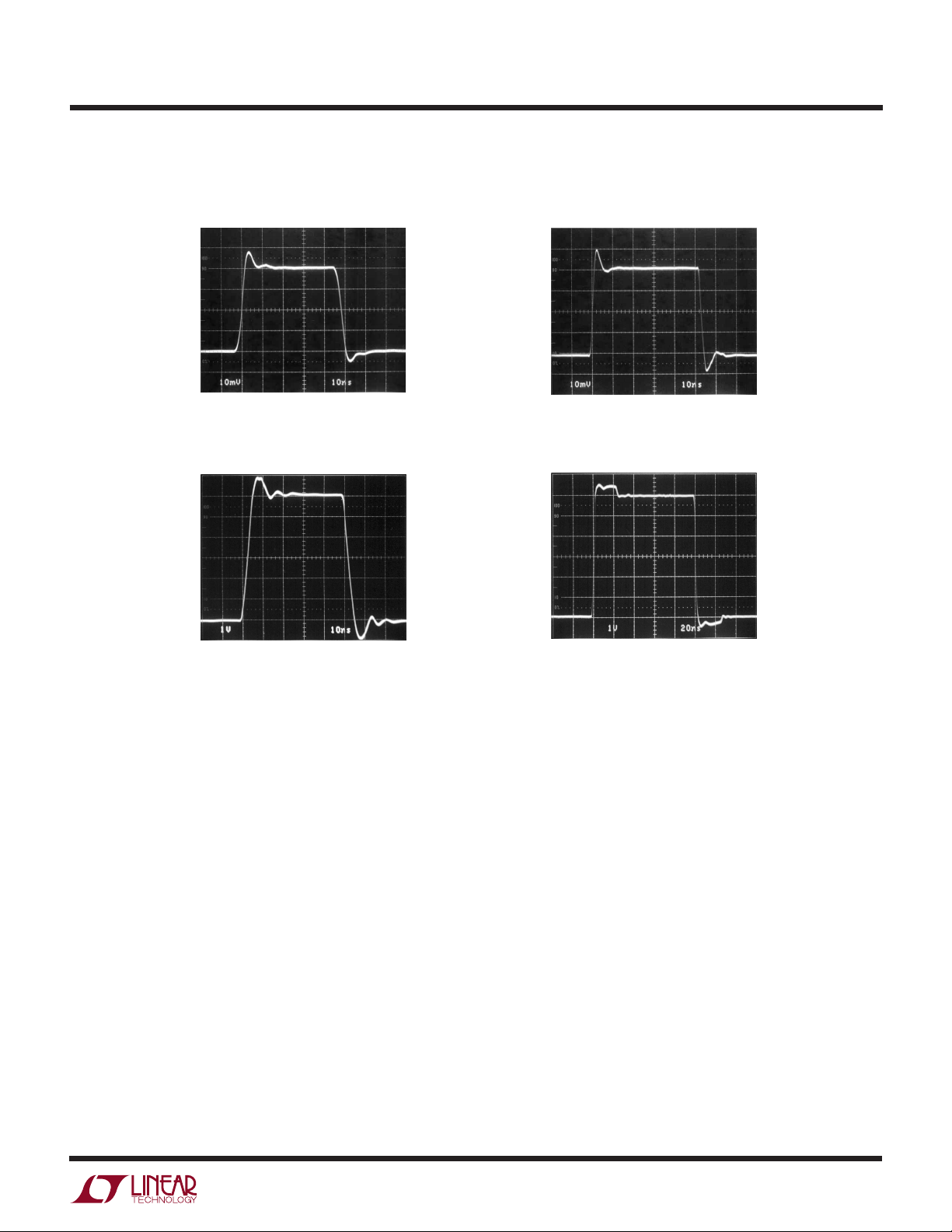
Small-Signal Transient,
AV = –1
Large-Signal Transient,
AV = –1, VS = ±5V
181567 G31
181567 G33
Small-Signal Transient,
AV = 1
181567 G32
Large-Signal Transient,
AV = 1, VS = ±5V
181567 G34
181567fa
11

LT1815
LT1816/LT1817
WUUU
APPLICATIO S I FOR ATIO
Layout and Passive Components
As with all high speed amplifiers, the LT1815/LT1816/
LT1817 require some attention to board layout. A ground
plane is recommended and trace lengths should be minimized, especially on the negative input lead.
Low ESL/ESR bypass capacitors should be placed directly
at the positive and negative supply (0.01µF ceramics are
recommended). For high drive current applications, additional 1µF to 10µF tantalums should be added.
The parallel combination of the feedback resistor and gain
setting resistor on the inverting input combine with the
input capacitance to form a pole that can cause peaking or
even oscillations. If feedback resistors greater than 1k are
used, a parallel capacitor of value:
CF > RG • CIN/R
should be used to cancel the input pole and optimize
dynamic performance. For applications where the DC
noise gain is 1 and a large feedback resistor is used, C
should be greater than or equal to CIN. An example would
be an I-to-V converter.
Input Considerations
The inputs of the LT1815/LT1816/LT1817 amplifiers are
connected to the base of an NPN and PNP bipolar transistor in parallel. The base currents are of opposite polarity
and provide first-order bias current cancellation. Due to
variation in the matching of NPN and PNP beta, the
polarity of the input bias current can be positive or
negative. The offset current, however, does not depend
on beta matching and is tightly controlled. Therefore, the
use of balanced source resistance at each input is recommended for applications where DC accuracy must be
maximized. For example, with a 100Ω source resistance
at each input, the 800nA maximum offset current results
in only 80µV of extra offset, while without balance the 8µA
maximum input bias current could result in a 0.8mV offset
contribution.
The inputs can withstand differential input voltages of up
to 6V without damage and without needing clamping or
series resistance for protection. This differential input
voltage generates a large internal current (up to 80mA),
F
F
which results in the high slew rate. In normal transient
closed-loop operation, this does not increase power
dissipation significantly because of the low duty cycle of
the transient inputs. Sustained differential inputs, however, will result in excessive power dissipation and therefore this device should not be used as a comparator
Capacitive Loading
The LT1815/LT1816/LT1817 are optimized for high bandwidth and low distortion applications. They can drive a
capacitive load of 10pF in a unity-gain configuration and
more with higher gain. When driving a larger capacitive
load, a resistor of 10Ω to 50Ω should be connected
between the output and the capacitive load to avoid ringing
or oscillation. The feedback should still be taken from the
output so that the resistor will isolate the capacitive load
to ensure stability.
Slew Rate
The slew rate of the LT1815/LT1816/LT1817 is proportional
to the differential input voltage. Therefore, highest slew rates
are seen in the lowest gain configurations. For example, a
5V output step in a gain of 10 has a 0.5V input step, whereas
in unity gain there is a 5V input step. The LT1815/LT1816/
LT1817 are tested for a slew rate in a gain of –1. Lower
slew rates occur in higher gain configurations.
Programmable Supply Current
(LT1815/LT1816A)
In order to operate the LT1815S6 or LT1816A at full speed
(and full supply current), connect the I
negative supply through a resistance of 75Ω or less.
To adjust or program the supply current and speed of the
LT1815S6 or LT1816A, connect an external resistor (R
between the I
Figure 1. The amplifiers are fully functional with 0 ≤ R
≤ 40k. Figures 2 and 3 show how the gain bandwidth and
supply current vary with the value of the programming
resistor R
section of the data sheet specifies maximum supply
current and offset voltage, as well as minimum gain
bandwidth and output current at the maximum R
of 40k.
pin and the negative supply as shown in
SET
. In addition, the Electrical Characteristics
SET
pin to the
SET
SET
.
SET
SET
value
)
12
181567fa

WUUU
APPLICATIO S I FOR ATIO
LT1815
LT1816/LT1817
5V
I
SET
R
SET
RL = 100Ω
+
V
–
V
181567 F01
VS = ±5V
T
A
RL = 500Ω
–5V
SET
= 25°C
181567 F02
–
LT1815S6
+
Figure 1. Programming Resistor Between I
250
200
150
100
GAIN BANDWIDTH (MHz)
50
0
10 1k 10k 40k
100
R
PROGRAMING RESISTOR (Ω)
SET
and V
Power Dissipation
The LT1815/LT1816/LT1817 combine high speed and
large output drive in small packages. It is possible to
exceed the maximum junction temperature specification
(150°C) under certain conditions. Maximum junction temperature (TJ) is calculated from the ambient temperature
(TA), power dissipation per amplifier (PD) and number of
amplifiers (n) as follows:
–
TJ = TA + (n • PD • θJA)
Power dissipation is composed of two parts. The first is
due to the quiescent supply current and the second is due
to on-chip dissipation caused by the load current. The worstcase load induced power occurs when the output voltage
is at 1/2 of either supply voltage (or the maximum swing
if less than 1/2 the supply voltage). Therefore P
P
= (V+ – V–) • (I
DMAX
P
= (V+ – V–) • (I
DMAX
(V
OMAX/RL
)
) + (V+/2)2/RL or
SMAX
) + (V+ – V
SMAX
OMAX
) •
DMAX
is:
Example: LT1816IS8 at 85°C, VS = ±5V, RL=100Ω
P
= (10V) • (11.5mA) + (2.5V)2/100Ω = 178mW
DMAX
Figure 2. Gain Bandwidth Product vs R
7
6
5
4
3
2
SUPPLY CURRENT (mA)
1
0
10 1k 10k 40k
100
R
PROGRAMMING RESISTOR (Ω)
SET
Figure 3. Supply Current vs R
SET
VS = ±5V
T
A
PER AMPLIFIER
Programming Resistor
SET
Programming Resistor
= 25°C
181567 F03
T
= 85°C + (2 • 178mW) • (150°C/W) = 138°C
JMAX
Circuit Operation
The LT1815/LT1816/LT1817 circuit topology is a true
voltage feedback amplifier that has the slewing behavior of
a current feedback amplifier. The operation of the circuit
can be understood by referring to the Simplified Schematic. Complementary NPN and PNP emitter followers
buffer the inputs and drive an internal resistor. The input
voltage appears across the resistor, generating current
that is mirrored into the high impedance node.
Complementary followers form an output stage that buffers the gain node from the load. The input resistor, input
stage transconductance and the capacitor on the high
impedance node determine the bandwidth. The slew rate
is determined by the current available to charge the gain
node capacitance. This current is the differential input
voltage divided by R1, so the slew rate is proportional to
the input step. Highest slew rates are therefore seen in the
lowest gain configurations.
181567fa
13

LT1815
LT1816/LT1817
WW
SI PLIFIED SCHE ATIC
+
V
BIAS
CONTROL
(one amplifier)
–IN
I
SET
–
V
LT1815S6/LT1816AMS ONLY
U
TYPICAL APPLICATIO S
R1
10k
R1
+IN
Two Op Amp Instrumentation Amplifier
R5
220Ω
R2
1k
R4
10k
OUT
C
181567 SS
14
–
1/2
LT1816
–
V
IN
+
+
1
12213
+
RRR
4
R
GAIN
=
3
R
TRIM R5 FOR GAIN
TRIM R1 FOR COMMON MODE REJECTION
BW = 2MHz
RR
()
+
+
4
R
R3
1k
23
+
5
R
–
1/2
LT1816
V
OUT
+
=
102
181567 TA03
181567fa
U
TYPICAL APPLICATIO S
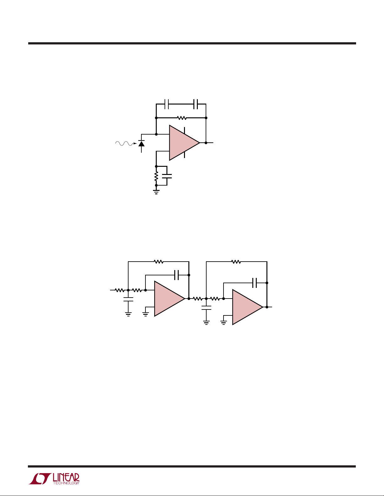
PHOTODIODE
SIEMENS/
INFINEON
SFH213
Photodiode Transimpedance Amplifier
1pF 1pF
4.75k
5V
–
LT1815
–5V
4.75k
+
0.01µF
OUTPUT OFFSET ≤1mV TYPICAL
BANDWIDTH = 30MHz
–5V
10% TO 90% RISE TIME = 22ns
OUTPUT NOISE (20MHz BW) = 300µV
181567 TA04
LT1815
LT1816/LT1817
P-P
4MHz, 4th Order Butterworth Filter
232Ω
47pF
665Ω
232Ω
V
IN
220pF
–
1/2 LT1816
+
274Ω
562Ω
470pF
274Ω
–
1/2 LT1816
+
22pF
V
OUT
181567 TA05
181567fa
15

LT1815
LT1816/LT1817
PACKAGE DESCRIPTIO
0.62
MAX
3.85 MAX
2.62 REF
RECOMMENDED SOLDER PAD LAYOUT
PER IPC CALCULATOR
0.20 BSC
DATUM ‘A’
U
S5 Package
5-Lead Plastic SOT-23
(Reference LTC DWG # 05-08-1633)
(Reference LTC DWG # 05-08-1635)
0.95
REF
1.22 REF
1.4 MIN
2.60 – 3.00
0.90 – 1.45
1.50 – 1.75
(NOTE 4)
PIN ONE
0.90 – 1.30
0.95 BSC
2.80 – 3.10
(NOTE 4)
0.25 – 0.50
TYP 5 PLCS
NOTE 3
0.00 – 0.15
NOTE:
1. DIMENSIONS ARE IN MILLIMETERS
2. DRAWING NOT TO SCALE
3. DIMENSIONS ARE INCLUSIVE OF PLATING
4. DIMENSIONS ARE EXCLUSIVE OF MOLD FLASH AND METAL BURR
5. MOLD FLASH SHALL NOT EXCEED 0.254mm
6. PACKAGE EIAJ REFERENCE IS SC-74A (EIAJ)
0.35 – 0.55 REF
0.09 – 0.20
(NOTE 3)
6-Lead Plastic SOT-23
(Reference LTC DWG # 05-08-1634)
(Reference LTC DWG # 05-08-1636)
3.85 MAX
0.20 BSC
0.62
MAX
2.62 REF
RECOMMENDED SOLDER PAD LAYOUT
PER IPC CALCULATOR
DATUM ‘A’
0.95
REF
1.22 REF
1.4 MIN
S6 Package
1.50 – 1.75
2.60 – 3.00
(NOTE 4)
0.90 – 1.45
1.90 BSC
ATTENTION: ORIGINAL SOT23-5L PACKAGE.
MOST SOT23-5L PRODUCTS CONVERTED TO THIN SOT23
PACKAGE, DRAWING # 05-08-1635 AFTER APPROXIMATELY
APRIL 2001 SHIP DATE
2.80 – 3.10
(NOTE 4)
PIN ONE ID
0.95 BSC
0.90 – 1.30
S5 SOT-23 0502
0.25 – 0.50
TYP 6 PLCS
NOTE 3
16
NOTE:
1. DIMENSIONS ARE IN MILLIMETERS
2. DRAWING NOT TO SCALE
3. DIMENSIONS ARE INCLUSIVE OF PLATING
4. DIMENSIONS ARE EXCLUSIVE OF MOLD FLASH AND METAL BURR
5. MOLD FLASH SHALL NOT EXCEED 0.254mm
6. PACKAGE EIAJ REFERENCE IS SC-74A (EIAJ)
0.35 – 0.55 REF
0.09 – 0.20
(NOTE 3)
1.90 BSC
ATTENTION: ORIGINAL SOT23-6L PACKAGE.
MOST SOT23-6L PRODUCTS CONVERTED TO THIN SOT23
PACKAGE, DRAWING # 05-08-1636 AFTER APPROXIMATELY
APRIL 2001 SHIP DATE
0.09 – 0.15
NOTE 3
S6 SOT-23 0502
181567fa

PACKAGE DESCRIPTIO
U
DD Package
8-Lead Plastic DFN (3mm × 3mm)
(Reference LTC DWG # 05-08-1698)
0.675 ±0.05
LT1815
LT1816/LT1817
R = 0.115
TYP
0.38 ± 0.10
85
3.5 ±0.05
1.65 ±0.05
(2 SIDES)2.15 ±0.05
PACKAGE
OUTLINE
0.28 ± 0.05
RECOMMENDED SOLDER PAD PITCH AND DIMENSIONS
0.50
BSC
2.38 ±0.05
(2 SIDES)
5.23
(.206)
MIN
0.42 ± 0.04
(.0165 ± .0015)
TYP
RECOMMENDED SOLDER PAD LAYOUT
DETAIL “A”
0.254
(.010)
GAUGE PLANE
0.18
(.077)
NOTE:
1. DIMENSIONS IN MILLIMETER/(INCH)
2. DRAWING NOT TO SCALE
3. DIMENSION DOES NOT INCLUDE MOLD FLASH, PROTRUSIONS OR GATE BURRS.
MOLD FLASH, PROTRUSIONS OR GATE BURRS SHALL NOT EXCEED 0.152mm (.006") PER SIDE
4. DIMENSION DOES NOT INCLUDE INTERLEAD FLASH OR PROTRUSIONS.
INTERLEAD FLASH OR PROTRUSIONS SHALL NOT EXCEED 0.152mm (.006") PER SIDE
5. LEAD COPLANARITY (BOTTOM OF LEADS AFTER FORMING) SHALL BE 0.102mm (.004") MAX
3.00 ±0.10
PIN 1
TOP MARK
0.200 REF
NOTE:
1. DRAWING TO BE MADE A JEDEC PACKAGE OUTLINE M0-229 VARIATION OF (WEED-1)
2. ALL DIMENSIONS ARE IN MILLIMETERS
3. DIMENSIONS OF EXPOSED PAD ON BOTTOM OF PACKAGE DO NOT INCLUDE
MOLD FLASH. MOLD FLASH, IF PRESENT, SHALL NOT EXCEED 0.15mm ON ANY SIDE
4. EXPOSED PAD SHALL BE SOLDER PLATED
(4 SIDES)
0.75 ±0.05
MS8 Package
8-Lead Plastic MSOP
(Reference LTC DWG # 05-08-1660)
0.889 ± 0.127
(.035 ± .005)
3.2 – 3.45
(.126 – .136)
3.00 ± 0.102
SEATING
PLANE
(.118 ± .004)
(NOTE 3)
4.90 ± 0.15
(1.93 ± .006)
0.22 – 0.38
(.009 – .015)
TYP
1.10
(.043)
MAX
12
0.65
(.0256)
BSC
8
(.0256)
0° – 6° TYP
DETAIL “A”
0.65
BSC
(.021 ± .006)
0.53 ± 0.015
0.00 – 0.05
7
6
5
3
4
1.65 ± 0.10
(2 SIDES)
0.28 ± 0.05
BOTTOM VIEW—EXPOSED PAD
0.52
(.206)
REF
3.00 ± 0.102
(.118 ± .004)
NOTE 4
0.86
(.034)
REF
0.13 ± 0.076
(.005 ± .003)
MSOP (MS8) 0802
2.38 ±0.10
(2 SIDES)
14
0.50 BSC
(DD8) DFN 0203
181567fa
17
LT1815
LT1816/LT1817
PACKAGE DESCRIPTIO
U
MS10 Package
10-Lead Plastic MSOP
(Reference LTC DWG # 05-08-1661)
0.889
± 0.127
(.035 ± .005)
5.23
(.206)
MIN
0.305 ± 0.038
(.0120 ± .0015)
TYP
RECOMMENDED SOLDER PAD LAYOUT
0.254
(.010)
GAUGE PLANE
0.18
(.007)
NOTE:
1. DIMENSIONS IN MILLIMETER/(INCH)
2. DRAWING NOT TO SCALE
3. DIMENSION DOES NOT INCLUDE MOLD FLASH, PROTRUSIONS OR GATE BURRS.
MOLD FLASH, PROTRUSIONS OR GATE BURRS SHALL NOT EXCEED 0.152mm (.006") PER SIDE
4. DIMENSION DOES NOT INCLUDE INTERLEAD FLASH OR PROTRUSIONS.
INTERLEAD FLASH OR PROTRUSIONS SHALL NOT EXCEED 0.152mm (.006") PER SIDE
5. LEAD COPLANARITY (BOTTOM OF LEADS AFTER FORMING) SHALL BE 0.102mm (.004") MAX
(.126 – .136)
DETAIL “A”
DETAIL “A”
3.2 – 3.45
0.50
(.0197)
BSC
° – 6° TYP
0
0.53 ± 0.01
(.021 ± .006)
SEATING
PLANE
3.00 ± 0.102
(.118 ± .004)
(NOTE 3)
4.90 ± 0.15
(1.93 ± .006)
0.17 – 0.27
(.007 – .011)
TYP
1.10
(.043)
MAX
S8 Package
8-Lead Plastic Small Outline (Narrow .150 Inch)
(Reference LTC DWG # 05-08-1610)
12
0.50
(.0197)
BSC
0.497 ± 0.076
7
6
45
(.0196 ± .003)
REF
3.00 ± 0.102
(.118 ± .004)
NOTE 4
0.86
(.034)
REF
0.13 ± 0.076
(.005 ± .003)
MSOP (MS) 0802
8910
3
18
.050 BSC
N
.245
MIN
1 2 3 N/2
.030 ±.005
TYP
RECOMMENDED SOLDER PAD LAYOUT
.010 – .020
(0.254 – 0.508)
.008 – .010
(0.203 – 0.254)
NOTE:
1. DIMENSIONS IN
2. DRAWING NOT TO SCALE
3. THESE DIMENSIONS DO NOT INCLUDE MOLD FLASH OR PROTRUSIONS.
MOLD FLASH OR PROTRUSIONS SHALL NOT EXCEED .006" (0.15mm)
× 45°
.016 – .050
(0.406 – 1.270)
INCHES
(MILLIMETERS)
.045 ±.005
.160 ±.005
(5.791 – 6.197)
0°– 8° TYP
.228 – .244
.053 – .069
(1.346 – 1.752)
(0.355 – 0.483)
.014 – .019
TYP
(4.801 – 5.004)
8
N
1
.189 – .197
NOTE 3
7
2
5
6
.150 – .157
(3.810 – 3.988)
NOTE 3
N/2
3
4
.004 – .010
(0.101 – 0.254)
.050
(1.270)
BSC
SO8 0502
181567fa

PACKAGE DESCRIPTIO
LT1815
LT1816/LT1817
U
S Package
14-Lead Plastic Small Outline (Narrow .150 Inch)
(Reference LTC DWG # 05-08-1610)
.050 BSC
N
.245
MIN
1 2 3 N/2
.030 ±.005
TYP
RECOMMENDED SOLDER PAD LAYOUT
.010 – .020
(0.254 – 0.508)
.008 – .010
(0.203 – 0.254)
NOTE:
1. DIMENSIONS IN
2. DRAWING NOT TO SCALE
3. THESE DIMENSIONS DO NOT INCLUDE MOLD FLASH OR PROTRUSIONS.
MOLD FLASH OR PROTRUSIONS SHALL NOT EXCEED .006" (0.15mm)
× 45°
.016 – .050
(0.406 – 1.270)
INCHES
(MILLIMETERS)
.045 ±.005
.160 ±.005
(5.791 – 6.197)
0° – 8° TYP
16-Lead Plastic SSOP (Narrow .150 Inch)
(Reference LTC DWG # 05-08-1641)
.045 ±.005
.228 – .244
.053 – .069
(1.346 – 1.752)
.014 – .019
(0.355 – 0.483)
GN Package
TYP
.337 – .344
(8.560 – 8.738)
13
14
N
1
2
NOTE 3
12
11 10
3
4
16
15
5
.050
(1.270)
BSC
.189 – .196*
(4.801 – 4.978)
14
13
9
6
12 11 10
8
N/2
7
9
.150 – .157
(3.810 – 3.988)
NOTE 3
.004 – .010
(0.101 – 0.254)
S14 0502
.009
(0.229)
REF
.254 MIN
RECOMMENDED SOLDER PAD LAYOUT
.007 – .0098
(0.178 – 0.249)
.016 – .050
NOTE:
1. CONTROLLING DIMENSION: INCHES
2. DIMENSIONS ARE IN
3. DRAWING NOT TO SCALE
*DIMENSION DOES NOT INCLUDE MOLD FLASH. MOLD FLASH
SHALL NOT EXCEED 0.006" (0.152mm) PER SIDE
**DIMENSION DOES NOT INCLUDE INTERLEAD FLASH. INTERLEAD
FLASH SHALL NOT EXCEED 0.010" (0.254mm) PER SIDE
(0.406 – 1.270)
(MILLIMETERS)
INCHES
.150 – .165
.0250 TYP.0165 ±.0015
.015 ± .004
(0.38 ± 0.10)
0° – 8° TYP
× 45°
.229 – .244
(5.817 – 6.198)
.053 – .068
(1.351 – 1.727)
.008 – .012
(0.203 – 0.305)
12
4
3
Information furnished by Linear Technology Corporation is believed to be accurate and reliable.
However, no responsibility is assumed for its use. Linear Technology Corporation makes no representation that the interconnection of its circuits as described herein will not infringe on existing patent rights.
5
678
.0250
(0.635)
BSC
.150 – .157**
(3.810 – 3.988)
.004 – .0098
(0.102 – 0.249)
GN16 (SSOP) 0502
181567fa
19

LT1815
LT1816/LT1817
U
TYPICAL APPLICATIO S
Bandpass Filter with Independently Settable Gain, Q and f
R1
–
1/4 LT1817
+
R
R
F
–
1/4 LT1817
+
C
–
1/4 LT1817
R
R
G
V
IN
–
1/4 LT1817
Q
R
+
R1
GAIN =
R
G
R1
Q =
f
C
R
Q
1
=
2πR
C
F
R
C
C
BANDPASS
OUT
R
F
+
181567 TA06a
455kHz Filter Frequency Response
R = 499Ω
0
R1 = 499Ω
= 511Ω
R
F
= 49.9Ω
R
Q
= 499Ω
R
G
C = 680pF
= 455kHz
f
C
Q = 10
GAIN = 1
OUTPUT MAGNITUDE (6dB/DIV)
100k 1M 10M
FREQUENCY (Hz)
VS = ±5V
= 5V
V
IN
DISTORTION:
2nd < –76dB
3rd < –90dB
ACROSS FREQ
RANGE
NOISE: ≈60µV
OVER 1MHz
BANDWIDTH
P-P
181567 TA06b
Differential DSL Receiver
5V
+
V
+ DRIVER
+
1/2 LT1816
–
DIFFERENTIAL
RECEIVE
SIGNAL
– DRIVER
PHONE
LINE
–
1/2 LT1816
+
V
–5V
181567 TA07
–
RELATED PARTS
PART NUMBER DESCRIPTION COMMENTS
LT1363/LT1364/LT1365 Single/Dual/Quad 70MHz, 1V/ns, C-LoadTM Op Amp Wide Supply Range: ±2.5V to ±15V
LT1395/LT1396/LT1397 Single/Dual/Quad 400MHz Current Feedback Amplifier 4.6mA Supply Current, 800V/µs, 80mA Output Current
LT1806/LT1807 Single/Dual 325MHz, 140V/µs Rail-to-Rail I/O Op Amp Low Noise: 3.5nV/√Hz
LT1809/LT1810 Single/Dual 180MHz, 350V/µs Rail-to-Rail I/O Op Amp Low Distortion: 90dBc at 5MHz
LT1812/LT1813/LT1814 Single/Dual/Quad 3mA, 100MHz, 750V/µs Op Amp Low Power: 3.6mA Max at ±5V
C-Load is a trademark of Linear Technology Corporation.
181567fa
LT/TP 0303 1K REV A • PRINTED IN USA
LINEAR TECHNO LOGY CORPORATION 2001
20
Linear Technology Corporation
1630 McCarthy Blvd., Milpitas, CA 95035-7417
(408) 432-1900 ● FAX: (408) 434-0507
●
www.linear.com
 Loading...