

Page 1
Application Note 79
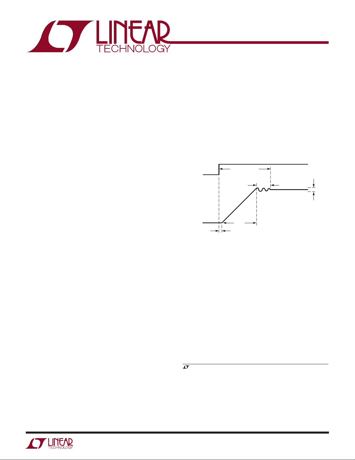
INPUT
OUTPUT
AN79 F01
SETTLING TIME
SLEW
TIME
RING TIME
ALLOWABLE
OUTPUT
ERROR
BAND
DELAY TIME
September 1999
30 Nanosecond Settling Time Measurement for a
Precision Wideband Amplifier
Quantifying Prompt Certainty
Jim Williams
Introduction
Instrumentation, waveform generation, data acquisition,
feedback control systems and other application areas
utilize wideband amplifiers. New components (see page 2
“A Precision Wideband Dual Amplifier with 30ns Settling
Time”) have introduced precision while maintaining high
speed operation. The amplifier’s DC and AC specifications
approach or equal previous devices at significantly lower
cost while saving power.
Settling Time Defined
Amplifier DC specifications are relatively easy to verify.
Measurement techniques are well understood, albeit often
tedious. AC specifications require more sophisticated
approaches to produce reliable information. In particular,
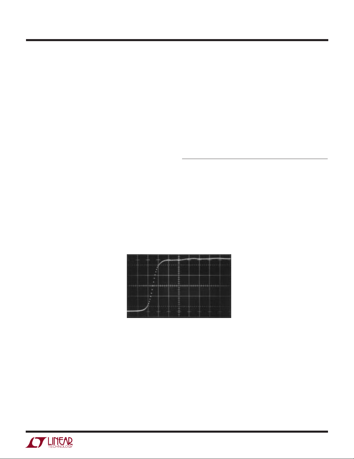
amplifier settling time is extraordinarily difficult to determine. Settling time is the elapsed time from input application until the output arrives at and remains within a
specified error band around the final value. It is usually
specified for a full-scale transition. Figure 1 shows that
settling time has three distinct components. The
time
is small and is almost entirely due to amplifier
delay
propagation delay. During this interval there is no output
movement. During
highest possible speed towards the final value.
slew time
the amplifier moves at its
Ring time
defines the region where the amplifier recovers from
slewing and ceases movement within some defined error
band. There is normally a trade-off between slew and ring
time. Fast slewing amplifiers generally have extended ring
times, complicating amplifier choice and frequency com-
Figure 1. Settling Time Components Include Delay, Slew and
Ring Times. Fast Amplifiers Reduce Slew Time, Although
Longer Ring Time Usually Results. Delay Time is Normally a
Small Term
pensation. Additionally, the architecture of very fast amplifiers usually dictates trade-offs which degrade DC error
1
terms.
Measuring anything at any speed requires care. Dynamic
measurement is particularly challenging. Reliable nanosecond region settling time measurement constitutes a
high order difficulty problem requiring exceptional care
in approach and experimental technique.
, LTC and LT are registered trademarks of Linear Technology Corporation.
Note 1: This issue is treated in detail in latter portions of the text.
Also see Appendix D “Practical Considerations for Amplifier
Compensation.
Note 2: The approach used for settling time measurement and its
description borrows heavily from a previous publication. See
Reference 1.
2
AN79-1
Page 2

Application Note 79
A PRECISION WIDEBAND DUAL AMPLIFIER WITH
30ns SETTLING TIME
Until recently, wideband amplifiers provided speed,
but sacrificed precision, power consumption and,
often, settling time. The LT®1813 dual op amp does not
require this compromise. It features low offset voltage
and bias current and high DC gain while operating at
low supply current. Settling time is 30ns to 0.1% for a
5V step. The output will drive a 100Ω load to ±3.5V
with ±5V supplies, and up to 100pF capacitive loading
is permissible. The table below provides short form
specifications.
LT1813 Short Form Specifications
CHARACTERISTIC SPECIFICATION
Offset Voltage 0.5mV
Offset Voltage vs Temperature 10µV/°C
Bias Current 1.5µA
DC Gain 3000
Noise Voltage 8nV/√Hz
Output Current 60mA
Slew Rate 750V/µs
Gain-Bandwidth 100MHz
Delay 2.5ns
Settling Time 30ns/0.1%
Supply Current 3mA per Amplifier
Considerations for Measuring Nanosecond Region
Settling Time
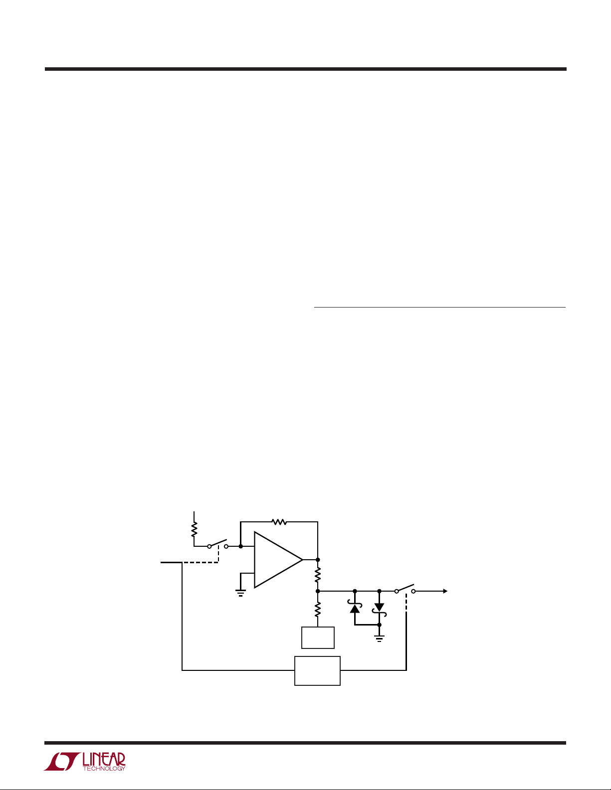
Historically, settling time has been measured with circuits
similar to that in Figure 2. The circuit uses the “false sum
node” technique. The resistors and amplifier form a bridge
type network. Assuming ideal resistors, the amplifier
output will step to –VIN when the input is driven. During
slew, the settle node is bounded by the diodes, limiting
voltage excursion. When settling occurs, the oscilloscope
probe voltage should be zero. Note that the resistor
divider’s attenuation means the probe’s output will be onehalf of the actual settled voltage.
In theory, this circuit allows settling to be observed to
small amplitudes. In practice, it cannot be relied upon to
produce useful measurements. Several flaws exist. The
circuit requires the input pulse to have a flat top within the
required measurement limits. Typically, settling within
5mV or less for a 5V step is of interest. No general purpose
pulse generator is meant to hold output amplitude and
noise within these limits. Generator output-caused aberrations appearing at the oscilloscope probe will be indistinguishable from amplifier output movement, producing
unreliable results. The oscilloscope connection also presents problems. As probe capacitance rises, AC loading of
the resistor junction influences observed settling waveforms. A 10pF probe alleviates this problem but its 10×
attenuation sacrifices oscilloscope gain. 1× probes are not
suitable because of their excessive input capacitance. An
AN79-2
INPUT STEP TO
OSCILLOSCOPE
POSITIVE INPUT
FROM PULSE
GENERATOR
Figure 2. Popular Summing Scheme for Settling Time Measurement Provides Misleading
Results. Pulse Generator Posttransition Aberrations Appear at Output. 10× Oscilloscope
Overdrive Occurs. Displayed Information Is Meaningless
–
AMPLIFIER
+
+V
REF
OUTPUT TO
OSCILLOSCOPE
AN79 F02
Page 3
Application Note 79
active 1× FET probe will work, but another issue remains.
The clamp diodes at the settle node are intended to reduce
swing during amplifier slewing, preventing excessive oscilloscope overdrive. Unfortunately, oscilloscope overdrive
recovery characteristics vary widely among different types
and are not usually specified. The Schottky diodes’ 400mV
drop means the oscilloscope will undergo an unacceptable overload, bringing displayed results into question.
3
At 0.1% resolution (5mV at the output—2.5mV at the
oscilloscope), the oscilloscope typically undergoes a 10×
overdrive at 10mV/DIV, and the desired 2.5mV baseline is
unattainable. At nanosecond speeds, the measurement
becomes hopeless with this arrangement. There is clearly
no chance of measurement integrity.
The preceding discussion indicates that measuring amplifier settling time requires an oscilloscope that is somehow
immune to overdrive and a “flat-top” pulse generator.
These become the central issues in wideband amplifier
settling time measurement.
The only oscilloscope technology that offers inherent
overdrive immunity is the classical sampling ‘scope.
4
Unfortunately, these instruments are no longer manufactured (although still available on the secondary market).
It is possible, however, to construct a circuit that borrows
the overload advantages of classical sampling ‘scope
technology. Additionally, the circuit can be endowed with
features particularly suited for measuring nanosecond
range settling time.
The “flat-top” pulse generator requirement can be avoided
by switching current, rather than voltage. It is much easier
to gate a quickly settling current into the amplifier’s
summing node than to control a voltage. This makes the
input pulse generator’s job easier, although it still must
have a rise time of 1 nanosecond or less to avoid measurement errors.
5
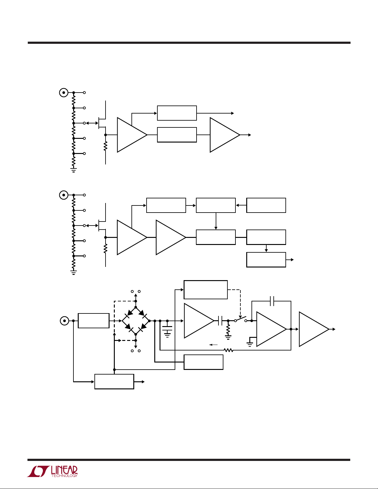
Practical Nanosecond Settling Time Measurement
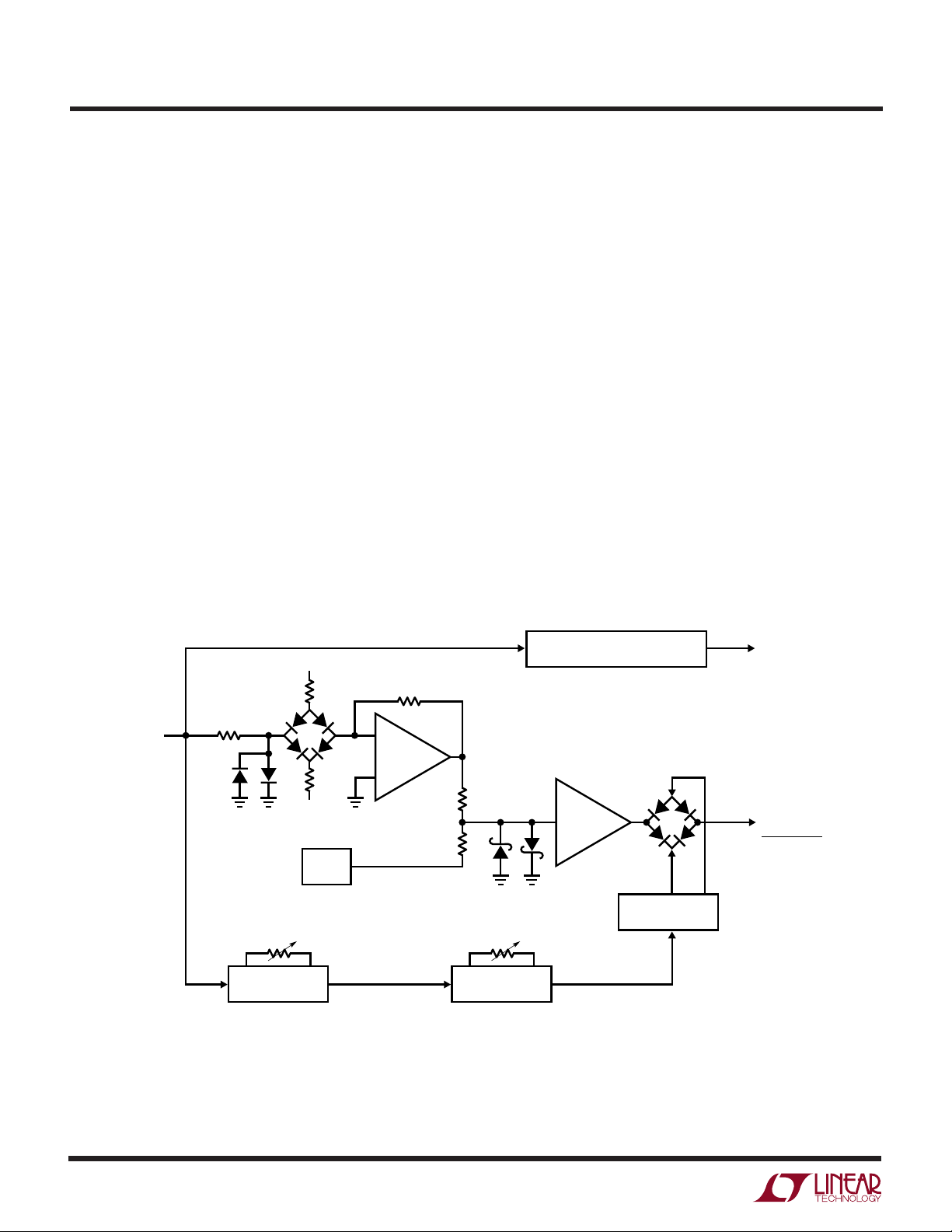
Figure 3 is a conceptual diagram of a settling time measurement circuit. This figure shares attributes with
Figure␣ 2, although some new features appear. In this case,
the oscilloscope is connected to the settle point by a
Note 3: For a discussion of oscilloscope overdrive considerations, see
Appendix A, “Evaluating Oscilloscope Overdrive Performance.”
Note 4: Classical sampling oscilloscopes should not be confused with
modern era digital sampling ‘scopes that have overdrive restrictions.
See Appendix A, “Evaluating Oscilloscope Overload Performance” for
comparisons of various type ‘scopes with respect to overdrive. For
detailed discussion of classical sampling ‘scope operation see
References 16 through 19 and 22 through 24. Reference 17 is
noteworthy; it is the most clearly written, concise explanation of
classical sampling instruments the author is aware of—a 12-page
jewel.
Note 5: Subnanosecond rise time pulse generators are considered in
Appendix B, “Subnanosecond Rise Time Pulse Generators for the Rich
and Poor.”
+V
CURRENT
SWITCH
INPUT FROM
PULSE
GENERATOR
Figure 3. Conceptual Arrangement is Insensitive to Pulse Generator Aberrations and Eliminates Oscilloscope
Overdrive. Switch at Input Gates Current Step to Amplifer. Second Switch is Controlled by Delayed Pulse
Generator, Preventing Oscilloscope from Monitoring Settle Node Until Settling is Nearly Complete
–
AMPLIFIER
+
SETTLE
NODE
–V
REF
DELAYED
PULSE
GENERATOR
SWITCH
AN79 F03
OUTPUT TO
OSCILLOSCOPE
AN79-3
Page 4
Application Note 79
switch. The switch state is determined by a delayed pulse
generator, which is triggered from the input pulse. The
delayed pulse generator’s timing is arranged so that the
switch does not close until settling is very nearly complete.
In this way the incoming waveform is sampled in time, as
well as amplitude. The oscilloscope is never subjected to
overdrive—no off-screen activity ever occurs.
A switch at the amplifier’s summing junction is controlled
by the input pulse. This switch gates current to the
amplifier via a voltage-driven resistor. This eliminates the
“flat-top” pulse generator requirement, although the switch
must be fast and devoid of drive artifacts.
Figure 4 is a more complete representation of the settling
time scheme. Figure 3’s blocks appear in greater detail
and some new refinements show up. The amplifier summing area is unchanged. Figure 3’s delayed pulse generator has been split into two blocks; a delay and a pulse
generator, both independently variable. The input step to
the oscilloscope runs through a section that compensates
for the propagation delay of the settling time measure-
ment path. The most striking new aspect of the diagram
are the diode bridge switches. Borrowed from classical
sampling oscilloscope circuitry, they are the key to the
measurement. The diode bridge’s inherent balance eliminates charge injection based errors. It is far superior to
other electronic switches in this character
istic. Any other
high speed switch technology contributes excessive output spikes due to charge-based feedthrough. FET switches
are not suitable because their gate-channel capacitance
permits such feedthrough. This capacitance allows gatedrive artifacts to corrupt switching, defeating the switches
purpose.
The diode bridge’s balance, combined with matched, low
capacitance monolithic diodes and high speed switching,
yields clean switching. The input-driven bridge switches
current into the amplifier’s summing point very quickly,
with settling inside a few nanoseconds. The diode clamp
to ground prevents excessive bridge drive swings and
ensures that input pulse characteristics are irrelevant.
TIME-CORRECTED
INPUT STEP TO
OSCILLOSCOPE
OUTPUT TO
OSCILLOSCOPE
SETTLE NODE
()
2
INPUT FROM
PULSE
GENERATOR
VARIABLE
DELAY
+V
–V
+V
REF
–
OUTPUT
AMPLIFIER
+
DELAYED
PULSE GENERATOR
0V TO 10V
TRANSITION
SETTLE
R
NODE
R
VARIABLE WIDTH
PULSE GENERATOR
DELAY COMPENSATION
SAMPLING
BRIDGE
DRIVER
×1
BRIDGE SWITCHING
CONTROL
SAMPLING
BRIDGE
SWITCH
AN79 F04
Figure 4. Block Diagram of Settling Time Measurement Scheme. Diode Bridge Switches Input Current to Amplifier.
Second Diode Bridge Switch Minimizes Switching Feedthrough, Preventing Oscilloscope Overdrive. Input Step
Time Reference is Compensated for Test Circuit Delays
AN79-4
Page 5
Application Note 79
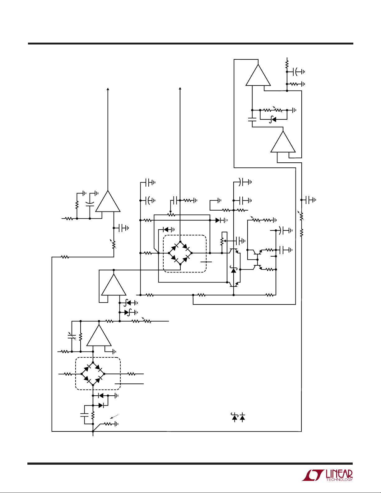
Figure 5 details considerations for the output diode bridge
switch. This bridge requires considerable attention to
achieve desired performance. The monolithic bridge
diodes tend to cancel each other’s temperature coefficient—drift is only about 100µV/°C—but a DC balance is
required to minimize offset.
DC balance is achieved by trimming the bridge on-current
for zero input-output offset voltage. Two AC trims are
required. The “AC balance” corrects for diode and layout
capacitive imbalances and the “skew compensation” corrects for any timing asymmetry in the nominally complementary bridge drive. These AC trims compensate small
dynamic imbalances, minimizing parasitic bridge outputs.
ON
OFF
+
–
V
V
AC BALANCE
ALL DIODES = CA3039
MONOLITHIC ARRAY
INPUT
DC BALANCE
SKEW
COMPENSATION
OUTPUT
AN79 F05
The input pulse triggers the C2-C3 based delayed pulse
generator. This circuitry is arranged to produce a delayed
(controllable by the 10k potentiometer) pulse whose width
(controllable by the 2k potentiometer) sets diode bridge
on-time. If the delay is set appropriately, the oscilloscope
will not see any input until settling is nearly complete,
eliminating overdrive. The sample window width is adjusted so that all remaining settling activity is observable.
In this way the oscilloscope’s output is reliable and meaningful data may be taken. The delayed generator’s output
is level shifted by the Q1-Q4 transistors, providing complementary switching drive to the bridge. The actual switching transistors, Q1-Q2, are UHF types, permitting true
differential bridge switching with less than 1ns of time
7
skew.
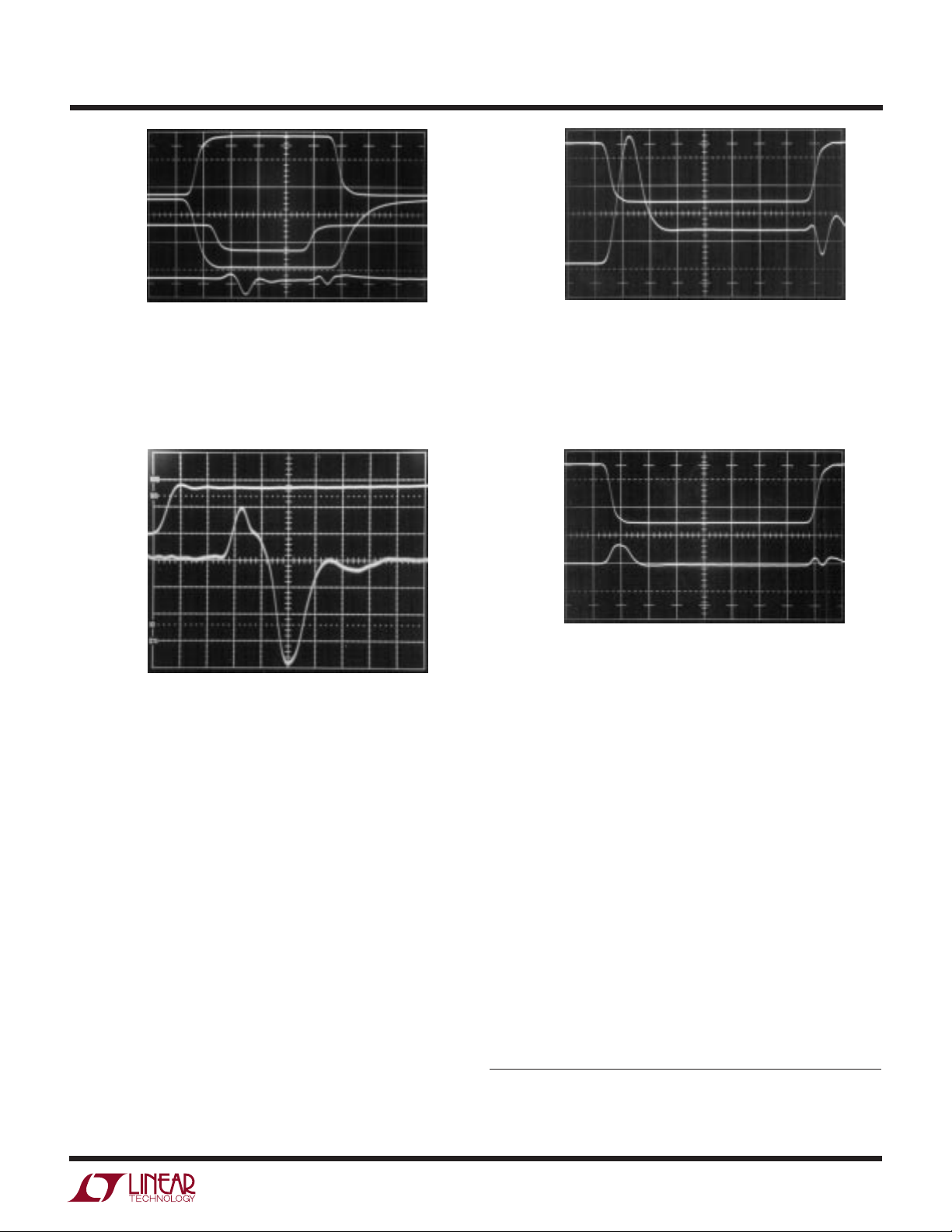
Figure 7 shows circuit waveforms. Trace A is the time-
corrected input pulse, trace B the amplifier output, trace C
the sample gate and trace D the settling time output. When
the sample gate goes low, the bridge switches cleanly, and
the last 10mV of slew are easily observed. Ring time is also
clearly visible, and the amplifier settles nicely to final value.
When the sample gate goes high, the bridge switches off,
with only millivolts of feedthrough. Note that there is no
off-screen activity at any time—the oscilloscope is never
subjected to overdrive.
–
+
V
V
ON
OFF
Figure 5. Diode Sampling Bridge Switch Trims Include
AC and DC Balance and Switch Drive Timing Skew
Detailed Settling Time Circuitry
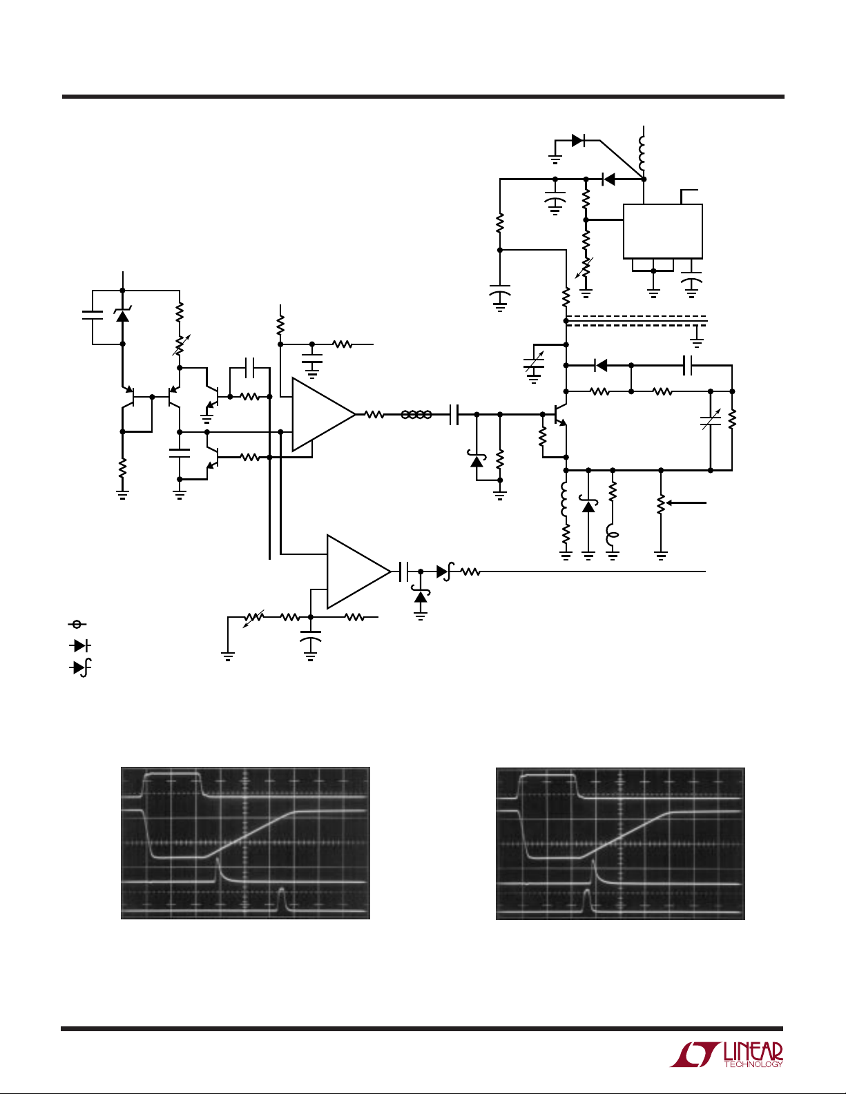
Figure 6 is a detailed schematic of the settling time
measurement circuitry. The input pulse switches the input
bridge and is also routed to the oscilloscope via a delaycompensation network. The delay network, composed of
a fast comparator and an adjustable RC network, compensates the oscilloscope’s input step signal for the 6ns delay
through the circuit’s measurement path.6 The amplifier’s
output is compared against the 5V reference via the
summing resistors. The 5V reference also furnishes the
bridge input current, making the measurement ratiometric.
The –5V reference supply pulls a current from the summing point, allowing the amplifier a 5V step from 2.5V to
–2.5V. The clamped settle node is unloaded by A1, which
drives the sampling bridge.
Figure 8 expands vertical and horizontal scales so that
settling detail is more visible.8 Trace A is the time-corrected input pulse and trace B the settling output. The last
15mV of slew (beginning at the center-screen vertical
marker) are easily observed, and the amplifier settles
inside 5mV (0.1%) in 30 nanoseconds.
The circuit requires trimming to achieve this level of
performance. DC and AC trims are required. Making these
adjustments requires disabling the amplifier (disconnect
the input current switch and the 1k resistor at the amplifier), and shorting the settle node directly to the ground
plane. Figure 9 shows typical results before trimming.
Note 6: See Appendix C, “Measuring and Compensating Settling
Circuit Delay.”
Note 7: The bridge switching scheme was developed at LTC by
George Feliz.
Note 8: In this and all following photos, settling time is measured from
the onset of the time-corrected input pulse. Additionally, settling signal
amplitude is calibrated with respect to the amplifier, not the sampling
bridge output. This eliminates ambiguity introduced by the summing
resistor’s ÷ 2 ratio.
AN79-5
Page 6
Application Note 79
+
AC
BALANCE
2.5k
TIME-CORRECTED
INPUT STEP TO
OSCILLOSCOPE
VIA HP-1120A
FET PROBE
SAMPLING BRIDGE
1k
SAMPLING
BRIDGE
DRIVER
8
1.1k
Q1
Q4
11
10
13
8
7
96
Q3
5pF
3pF
0.1µF
10pF
10µF
510Ω
100Ω
100Ω
2k
SAMPLE
WINDOW
WIDTH
10pF
Q2
CA3039
ARRAY
13
–5V
–5V
–5V
SKEW COMP
2.5k
2
7
11
10
4
3
5
2.2k
1.1k
5V
2.2k
10µF
1µF
0.1µF
470Ω
560Ω
51Ω
820Ω 51Ω
680Ω
500Ω
BASELINE
ZERO
5V
OUTPUT TO
OSCILLOSCOPE
VIA HP-1120A
FET PROBE
–
+
–
+
A1
LT1813
–
+
C1
1/2 LT1720
LT1813
0.1µF10µF
+
: 1N4148
: 1N5711
DIODE BRIDGES: HARRIS CA3039M
* = 1% FILM RESISTOR
Q1, Q2: MRF-501
Q3, Q4: LM3045 ARRAY
USE IN-LINE COAXIAL TERMINATOR FOR
PULSE GENERATOR INPUT. DO NOT MOUNT
50Ω RESISTOR ON BOARD
DERIVE 5V AND –5V SUPPLIES FROM
±15V.
USE LT317A FOR 5V, LT1175-5 FOR –5V
CONSTRUCTION IS CRITICAL—SEE TEXT
+
1µF
+
5V
DELAY COMPENSATION = 6ns
2k
2k
SAMPLE DELAY/WINDOW GENERATOR
SAMPLE GATE LINE
5V
3.9pF
DELAY
COMP
2k
2k
1k
10k
SAMPLE
DELAY
AN79 F06
909Ω*
499Ω*
2pF TO 8pF (SEE TEXT)
200Ω
SETTLE
NODE
SETTLE
NODE
ZERO
1k*
7
8
2pF
11
5V
CURRENT
SWITCH
–5V
AMPLIFIER
UNDER TEST
–5V
430Ω*
1k*
270Ω
50Ω
2
10
4
CA3039
ARRAY
PULSE
GENERATOR
INPUT
3
5
–
+
C3
1/2 LT1720
–
+
C2
+
13
–5V
INLINE
TERMINATION
(SEE TEXT
AND NOTES)
1/2 LT1720
430Ω*
ttention to Layout
AN79-6
Figure 6. Detailed Schematic of Settling Time Measurement Circuit Closely Follows Block Diagram. Optimum Performance Requires A
Page 7
Application Note 79
A = 2V/DIV
B = 2V/DIV
C = 5V/DIV
D = 20mV/DIV
20ns/DIV
Figure 7. Settling Time Circuit Waveforms Include TimeCorrected Input Pulse (Trace A), Amplifier-Under-Test Output
(Trace B), Sample Gate (Trace C) and Settling Time Output
(Trace D). Sample Gate Window’s Delay and Width are Variable
A = 2V/DIV
B = 5mV/DIV
AN79 F07
A = 2V/DIV
B = 5mV/DIV
10ns/DIV
Figure 9. Settling Time Circuit’s Output (Trace B) with
Unadjusted Sampling Bridge AC and DC Trims. Settle Node is
Grounded for This Test. Excessive Switch Drive Feedthrough and
Baseline Offset are Present. Trace A is the Sample Gate
A = 2V/DIV
B = 5mV/DIV
10ns/DIV
AN79 F09
AN79 F10
5ns/DIV AN79 F08
Figure 8. Expanded Vertical and Horizontal Scales Show
30ns Amplifier Settling Within 5mV (Trace B). Trace A is
Time-Corrected Input Step
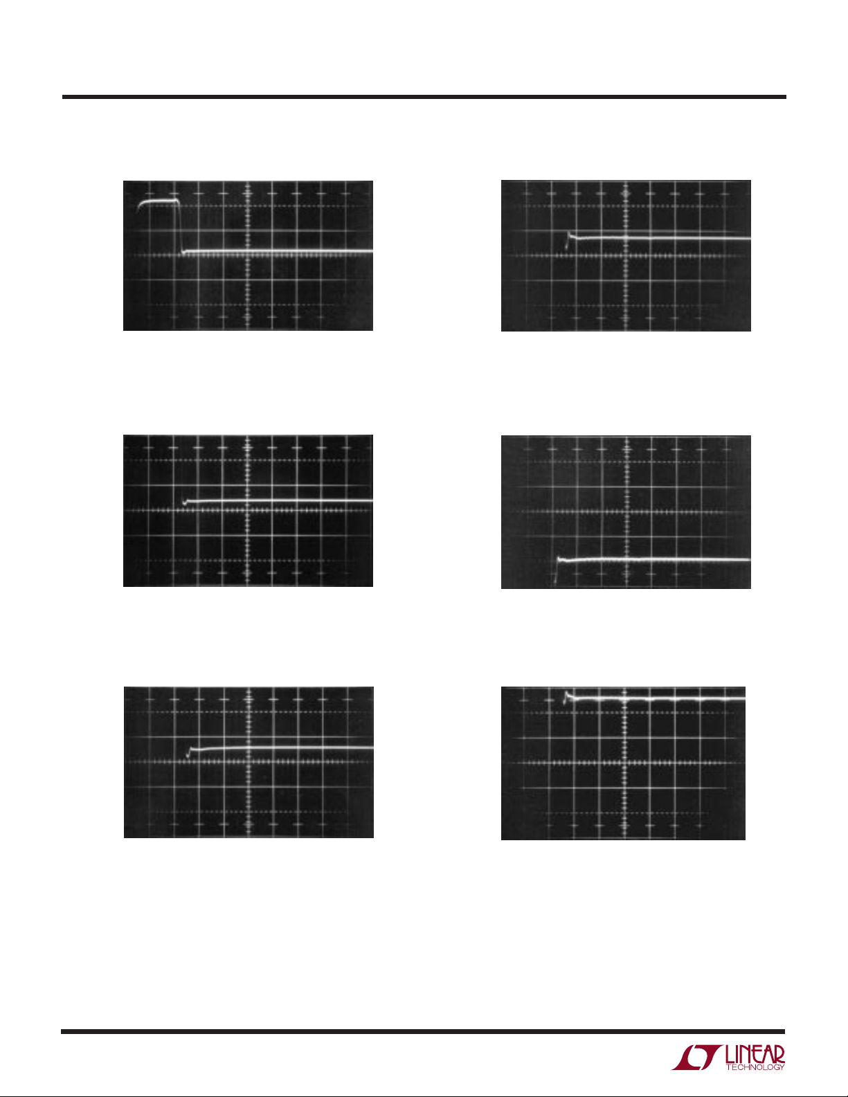
Trace A is the input pulse and trace B the settle signal
output. With the amplifier disabled and the settle node
grounded, the output should (theoretically) always be
zero. The photo shows this is not the case for an untrimmed bridge. AC and DC errors are present. The sample
gate’s transitions cause large swings. Additionally, the
output shows significant DC offset error during the sampling interval. Adjusting the AC balance and skew compensation minimizes the switching induced transients. The
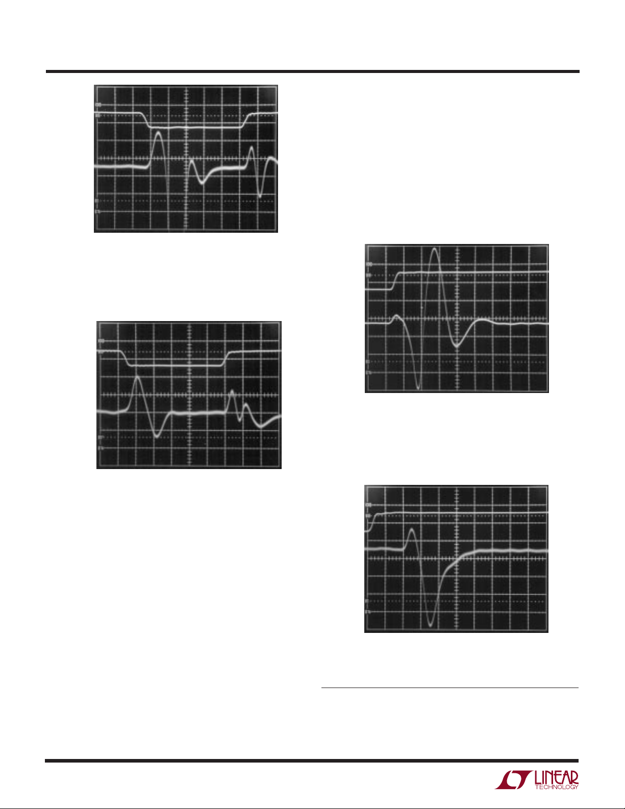
DC offset is adjusted out with the baseline zero trim. Figure
10 shows the results after making these adjustments. All
switching related activity is minimized and offset error
reduced to unreadable levels. Once this level of performance has been achieved, the circuit is nearly ready for
use.9 Unground the settle node and restore the current
switch and resistor connections to the amplifier. Any
Figure 10. Settling Time Circuit’s Output (Trace B) with
Sampling Bridge Trimmed. As in Figure 9, Settle Node is
Grounded for This Test. Switch Drive Feedthrough and
Baseline Offset are Minimized. Trace A is the Sample Gate
further differences between pre- and postsettling baseline
are corrected with the “settle node zero” trim.
Using the Sampling-Based Settling Time Circuit
Figures 11 and 12 underscore the importance of positioning the sampling window properly in time. In Figure 10 the
sample gate delay initiates the sample window (trace A)
too early and the residue amplifier’s output (trace B)
overdrives the oscilloscope when sampling commences.
Figure 12 is better, with no off-screen activity. All amplifier
settling residue is well inside the screen boundaries.
Note 9: Achieving this level of performance also depends on layout.
The circuit’s construction involves a number of subtleties and is
absolutely crucial. Please see Appendix E, “Breadboarding, Layout and
Connection Techniques.”
AN79-7
Page 8
Application Note 79
A = 5V/DIV
B = 5mV/DIV
very light compensation. Trace A is the time-corrected
input pulse and trace B the settling residue output. The
light compensation permits very fast slewing but excessive ringing amplitude over a protracted time results.
When sampling is initiated (just prior to the fourth vertical
division) the ringing is seen to be in its final stages,
although still offensive. Total settling time is about 43ns.
Figure 14 presents the opposite extreme. Here a large
value compensation capacitor eliminates all ringing but
slows down the amplifier so much that settling stretches
10ns/DIV
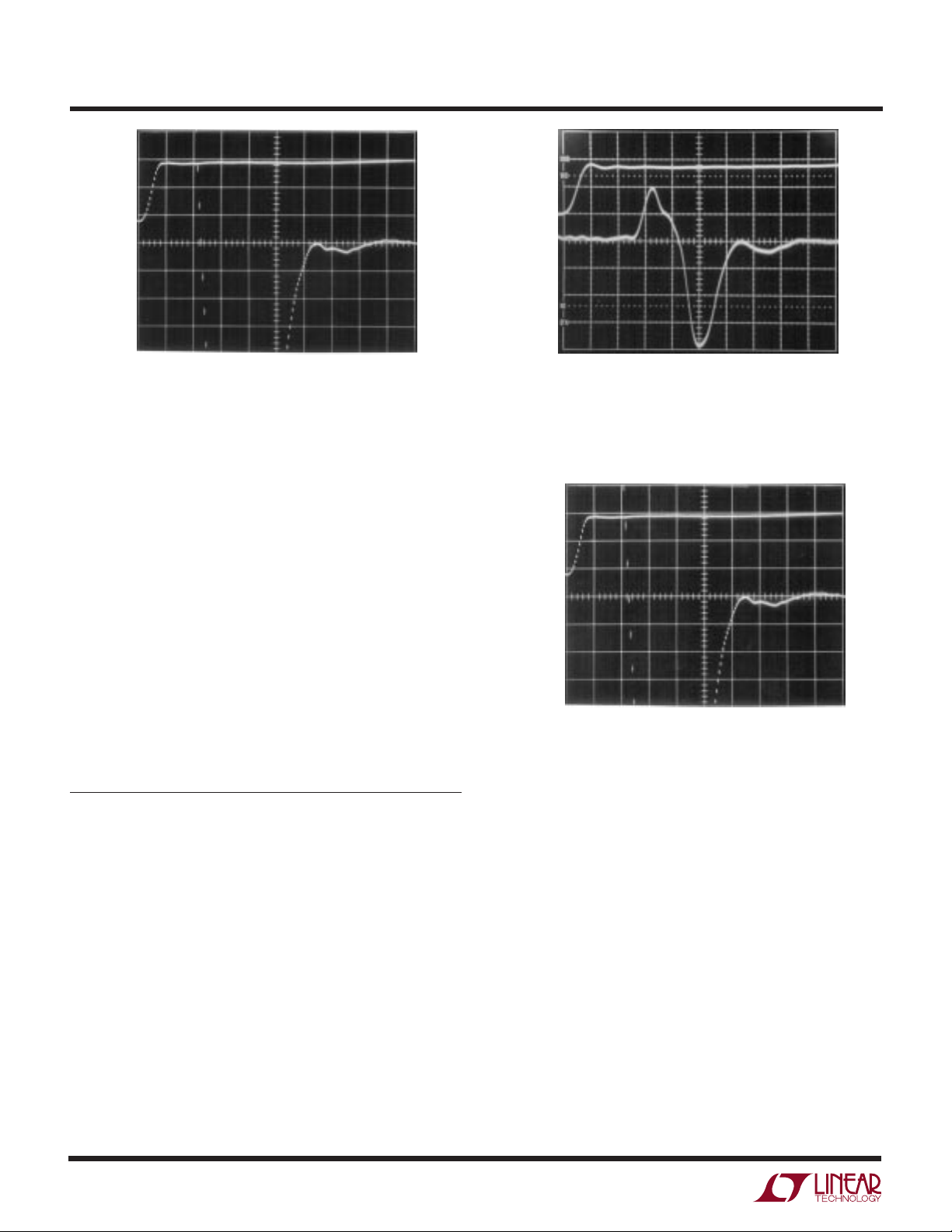
Figure 11. Oscilloscope Display with Inadequate Sample Gate
Delay. Sample Window (Trace A) Occurs Too Early, Resulting in
Off-Screen Activity in Settle Output (Trace B). Oscilloscope is
Overdriven, Making Displayed Information Questionable
A = 5V/DIV
B = 5mV/DIV
10ns/DIV AN79 F12
Figure 12. Optimal Sample Gate Delay Positions Sampling
Window (Trace A) So All Settle Output (Trace B) Information
is Well Inside Screen Boundaries
AN79 F11
A = 5V/DIV
B = 10mV/DIV
10ns/DIV AN79 F13
Figure 13. Settling Profile with Inadequate Feedback
Capacitance Shows Underdamped Response. Trace A is TimeCorrected Input Pulse. Trace B is Settling Residue Output.
t
= 43ns
SETTLE
A = 5V/DIV
In general, it is good practice to “walk” the sampling
window up to the last ten millivolts or so of amplifier
slewing so that the onset of ring time is observable. The
sampling based approach provides this capability and it is
a very powerful measurement tool. Additionally, remember that slower amplifiers may require extended delay and/
or sampling window times. This may necessitate larger
capacitor values in the delayed pulse generator timing
networks.
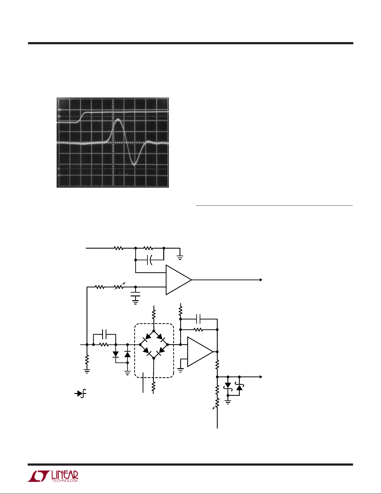
Compensation Capacitor Effects
The amplifier requires frequency compensation to get the
best possible settling time.10 Figure 13 shows effects of
AN79-8
B = 10mV/DIV
10ns/DIV
Figure 14. Excessive Feedback Capacitance Overdamps
Response. t
Note 10: This section discusses frequency compensation of the
amplifier within the context of sampling-based settling time measurement. As such, it is necessarily brief. Considerably more detail is
available in Appendix D, “Practical Considerations for Amplifier
Compensation.”
SETTLE
= 50ns
AN79 F14
Page 9
Application Note 79
out to 50ns. The best case appears in Figure 15. This photo
was taken with the compensation capacitor carefully chosen for the best possible settling time. Damping is tightly
controlled and settling time goes down to 30ns.
A = 5V/DIV
B = 5mV/DIV
5ns/DIV AN79 F15
Figure 15. Optimal Feedback Capacitance Yields Tightly Damped
Signature and Best Settling Time. Optimum Response Allows
Expanded Horizontal and Vertical Scales. t
SETTLE
≤ 30ns
Verifying Results—Alternate Method
The sampling-based settling time circuit appears to be a
useful measurement solution. How can its results be
tested to ensure confidence? A good way is to make the
same measurement with an alternate method and see if
results agree. It was stated earlier that classical sampling
oscilloscopes were inherently immune to overdrive.11 If
this is so, why not utilize this feature and attempt settling
time measurement directly at the clamped settle node?
Figure 16 does this. Under these conditions, the sampling
‘scope12 is heavily overdriven, but is ostensibly immune to
the insult. Figure 17 puts the sampling oscilloscope to the
test. Trace A is the time corrected input pulse and trace B
the settle signal. Despite a brutal overdrive, the ‘scope
appears to respond cleanly, giving a very plausible settle
signal presentation.
Note 11: See Appendix A, “Evaluating Oscilloscope Overdrive
Performance,” for in-depth discussion.
Note 12: Tektronix type 661 with 4S1 vertical and 5T3 timing plug-ins.
PULSE
GENERATOR
INPUT
* = 1% FILM RESISTOR
5V
100Ω
50Ω
: 1N5711
2pF
510Ω
2k
DELAY
COMP
1k
2
8
2k
+
1µF
3.9pF
13
7
3
–5V–5V
5V
11
430 Ω*
4
CA3039
ARRAY
430Ω*
–
1/2 LT1720
+
–5V
10
5
1k*
TYP 2.2pF (SEE TEXT)
C
COMP
510Ω*
–
LT1813
+
909Ω*
200Ω
SETTLE
NODE
ZERO
TIME-CORRECTED INPUT
STEP TO TEKTRONIX 661
OSCILLOSCOPE VIA
×10 HP-1120A FET PROBE
1k*
OUTPUT TO
TEKTRONIX 661 OSCILLOSCOPE
VIA ×1 HP-1120A FET PROBE
5V
AN79 F16
Figure 16. Settling Time Test Circuit Using Classical Sampling Oscilloscope.
Sampling ‘Scope’s Inherent Overload Immunity Permits Large Off-Screen Excursions
AN79-9
Page 10
Application Note 79
A = 2V/DIV
B = 5mV/DIV
5ns/DIV AN79 F17
Figure 17. Settling Time Measurement with the Classical
Sampling ‘Scope. Oscilloscope’s Overload Immunity Allows
Accurate Measurement Despite Extreme Overdrive
Summary of Results
The simplest way to summarize the different method’s
results is by visual comparison. Figures 18 and 19 repeat
previous photos of the two different settling-time methods. If both approaches represent good measurement
technique and are properly constructed, results should be
indentical.13 If this is the case, the identical data produced
by the two methods has a high probability of being valid.
A = 2V/DIV
B = 5mV/DIV
5ns/DIV AN79 F18
Figure 18. Settling Time Measurement Using the Sampling
Bridge Circuit. t
A = 2V/DIV
B = 5mV/DIV
SETTLE
= 30ns
Examination of the photographs shows nearly identical
settling times and settling waveform signatures. The shape
of the settling waveform is essentially identical in both
photos.14 This kind of agreement provides a high degree
of credibility to the measured results.
Note 13: Construction details of the settling time fixtures discussed
here appear (literally) in Appendix E, “Breadboarding, Layout and
Connection Techniques.”
Note 14: The slightly rougher appearance of figure 19’s final settling
movement (7th through 9th vertical divisions) may be due to the
sampling ‘scope’s substantially higher bandwidth. Figure 18 was taken
with a150MHz instrument; sampling oscilloscope bandwidth is 1GHz.
5ns/DIV
AN79 F19
Figure 19. Settling Time Measurement using the Classical
Sampling ‘Scope. t
SETTLE
= 30ns
AN79-10
Page 11

REFERENCES
Application Note 79
1. Williams, Jim, “Component and Measurement
Advances Ensure 16-Bit DAC Settling Time,” Linear
Technology Corporation, Application Note 74, July
1998.
2. Williams, Jim, “Measuring 16-Bit Settling Times:
The Art of Timely Accuracy,”
1998.
3. Williams, Jim, “Methods for Measuring Op Amp
Settling Time,” Linear Technology Corporation,
Application Note 10, July 1985.
4. Demerow, R., “Settling Time of Operational Amplifiers,”
Analog Dialogue
Inc., 1970.
5. Pease, R. A., “The Subtleties of Settling Time,”
, Volume 4-1, Analog Devices,
New Lightning Empiricist
1971.
6. Harvey, Barry, “Take the Guesswork Out of Settling
Time Measurements,”
7. Williams, Jim, “Settling Time Measurement
Demands Precise Test Circuitry,”
15, 1984.
8. Schoenwetter, H. R., “High-Accuracy Settling Time
Measurements,”
tion and Measurement
1983.
9. Sheingold, D. H., “DAC Settling Time Measurement,”
pg. 312-317. Prentice-Hall, 1986.
Analog-Digital Conversion Handbook
IEEE Transactions on Instrumenta-
, Vol. IM-32. No. 1, March
EDN
, November 19,
, Teledyne Philbrick, June
EDN
, September 19, 1985.
EDN
, November
,
The
14. Harris Semiconductor, “CA3039 Diode Array Data
Sheet,” Harris Semiconductor, 1993.
15. Korn, G. A. and Korn, T. M., “Electronic Analog and
Hybrid Computers,” “Diode Switches,” pg. 223-226.
McGraw-Hill, 1964.
16. Carlson, R., “A Versatile New DC-500MHz Oscilloscope with High Sensitivity and Dual Channel
Display,”
Company, January 1960.
17. Tektronix, Inc., “Sampling Notes,” Tektronix, Inc.,
1964.
18. Tektronix, Inc., “Type 1S1 Sampling Plug-In Operating and Service Manual,” Tektronix, Inc., 1965.
19. Mulvey, J., “Sampling Oscilloscope Circuits,”
Tektronix, Inc., Concept Series, 1970.
20. Addis, John, “Sampling Oscilloscopes,” Private
Communication, February, 1991.
21. Williams, Jim, “Bridge Circuits—Marrying Gain and
Balance,” Linear Technology Corporation, Application Note 43, June, 1990.
22. Tektronix, Inc., “Type 661 Sampling Oscilloscope
Operating and Service Manual,’ Tektronix, Inc.,
1963.
23. Tektronix, Inc., “Type 4S1 Sampling Plug-In Operating and Service Manual,” Tektronix, Inc., 1963.
24. Tektronix, Inc., “Type 5T3 Timing Unit Operating
and Service Manual,” Tektronix, Inc., 1965.
Hewlett-Packard Journal
, Hewlett-Packard
10. Orwiler, Bob, “Oscilloscope Vertical Amplifiers,”
Tektronix, Inc., Concept Series, 1969.
11. Addis, John, “Fast Vertical Amplifiers and Good
Engineering,”
and Personalities
12. W. Travis, “Settling Time Measurement Using
Delayed Switch,” Private Communication. 1984.
13. Hewlett-Packard, “Schottky Diodes for HighVolume, Low Cost Applications,” Application Note
942, Hewlett-Packard Company, 1973.
Analog Circuit Design; Art, Science
, Butterworths, 1991.
25. D. J. Hamilton, F. H. Shaver, P. G. Griffith,
“Avalanche Transistor Circuits for Generating
Rectangular Pulses,”
December, 1962.
26. R. B. Seeds, “Triggering of Avalanche Transistor
Pulse Circuits,” Technical Report No. 1653-1,
August 5, 1960,
Stanford Electronics Laboratories, Stanford
University, Stanford, California.
Electronic Engineering
,
Solid-State Electronics Laboratory
AN79-11
,
Page 12

Application Note 79
27. Haas, Isy, “Millimicrosecond Avalanche Switching
Circuit Utilizing Double-Diffused Silicon Transistors,” Fairchild Semiconductor,
(December 1961)
28. Beeson, R. H. Haas, I., Grinich, V. H., “Thermal
Response of Transistors in the Avalanche Mode,”
Fairchild Semiconductor, Technical Paper 6 (October 1959)
29. Tektronix, Inc., Type 111 Pretrigger Pulse Generator
Operating and Service Manual, Tektronix, Inc.
(1960)
30. G. B. B. Chaplin, “A Method of Designing Transistor
Avalanche Circuits with Applications to a Sensitive
Transistor Oscilloscope,” paper presented at the
1958 IRE-AIEE Solid State Circuits Conference,
Philadelphia, Penn., February 1958.
Application Note 8/2
31. Motorola, Inc., “Avalanche Mode Switching,”
Chapter 9, pp 285-304.
book
, 1963.
32. Williams, Jim, “A Seven-Nanosecond Comparator
for Single Supply Operation,” “Programmable, SubNanosecond Delayed Pulse Generator,” pg. 32-34,
Linear Technology Corporation, Application Note
72, 1998.
33. Morrison, Ralph, “Grounding and Shielding
Techniques in Instrumentation,” 2nd Edition,
Wiley Interscience
34. Ott, Henry W., “Noise Reduction Techniques in
Electronic Systems,”
35. Williams, Jim, “High Speed Amplifier Techniques,”
Linear Technology Corporation, Application Note
47. 1991.
Motorola Transistor Hand-
, 1977.
Wiley Interscience
, 1976.
AN79-12
Page 13

APPENDIX A
EVALUATING OSCILLOSCOPE OVERDRIVE
PERFORMANCE
Application Note 79
The sampling bridge-based settling time circuit is heavily
oriented towards preventing overdrive to the monitoring
oscilloscope. This is done to avoid overdriving the oscilloscope. Oscilloscope recovery from overdrive is a grey
area and almost never specified. How long must one wait
after an overdrive before the display can be taken seriously?
The answer to this question is quite complex. Factors involved include the degree of overdrive, its duty cycle, its
magnitude in time and amplitude and other considerations.
Oscilloscope response to overdrive varies widely between
types and markedly different behavior can be observed in
any individual instrument. For example, the recovery time
for a 100× overload at 0.005V/DIV may be very different
than at 0.1V/DIV. The recovery characteristic may also vary
with waveform shape, DC content and repetition rate. With
so many variables, it is clear that measurements involving
oscilloscope overdrive must be approached with caution.
Why do most oscilloscopes have so much trouble recovering from overdrive? The answer to this question
requires some study of the three basic oscilloscope types’
vertical paths. The types include analog (Figure A1A),
digital (Figure A1B) and classical sampling (Figure A1C)
oscilloscopes. Analog and digital ‘scopes are susceptible
to overdrive. The classical sampling ‘scope is the only
architecture that is inherently immune to overdrive.
An analog oscilloscope (Figure A1A) is a real time, continuous linear system.1 The input is applied to an attenuator, which is unloaded by a wideband buffer. The vertical
preamp provides gain, and drives the trigger pick-off,
delay line and the vertical output amplifier. The attenuator
and delay line are passive elements and require little
comment. The buffer, preamp and vertical output amplifier are complex linear gain blocks, each with dynamic
operating range restrictions. Additionally, the operating
point of each block may be set by inherent circuit balance,
low frequency stabilization paths or both. When the input
is overdriven, one or more of these stages may saturate,
forcing internal nodes and components to abnormal operating points and temperatures. When the overload ceases,
full recovery of the electronic and thermal time constants
may require surprising lengths of time.
2
The digital sampling oscilloscope (Figure A1B) eliminates
the vertical output amplifier, but has an attenuator buffer
and amplifiers ahead of the A/D converter. Because of this,
it is similarly susceptible to overdrive recovery problems.
The classical sampling oscilloscope is unique. Its nature
of operation makes it inherently immune to overload. Figure A1C shows why. The sampling occurs
before
any gain
is taken in the system. Unlike Figure A1B’s digitally sampled
‘scope, the input is fully passive to the sampling point.
Additionally, the output is fed back to the sampling bridge,
maintaining its operating point over a very wide range of
inputs. The dynamic swing available to maintain the bridge
output is large and easily accommodates a wide range of
oscilloscope inputs. Because of all this, the amplifiers in
this instrument do not see overload, even at 1000× overdrives, and there is no recovery problem. Additional immunity derives from the instrument’s relatively slow sample
rate—even if the amplifiers were overloaded, they would
have plenty of time to recover between samples.
3
The designers of classical sampling ‘scopes capitalized on
the overdrive immunity by including variable DC offset
generators to bias the feedback loop (see Figure A1C,
lower right). This permits the user to offset a large input,
so small amplitude activity on top of the signal can be
accurately observed. This is ideal for, among other things,
settling time measurements. Unfortunately, classical sampling oscilloscopes are no longer manufactured, so if you
have one, take care of it!
Note 1: Ergo, the Real Thing. Hopelessly bigoted residents of this
locale mourn the passing of the analog ‘scope era and frantically hoard
every instrument they can find.
Note 2: Some discussion of input overdrive effects in analog oscilloscope circuitry is found in Reference 11.
Note 3: Additional information and detailed treatment of classical
sampling oscilloscope operation appears in References 16–19 and
22–24.
Note 4: Modern variants of the classical architecture (e.g., Tektronix
11801B) may provide similar capability, although we have not tried
them.
4
AN79-13
Page 14

Application Note 79
Although analog and digital oscilloscopes are susceptible
to overdrive, many types can tolerate some degree of this
abuse. The early portion of this appendix stressed that
measurements involving oscilloscope overdrive must be
approached with caution. Nevertheless, a simple test can
indicate when the oscilloscope is being deleteriously affected by overdrive.
The waveform to be expanded is placed on the screen at a
vertical sensitivity that eliminates all off-screen activity.
Figure A2 shows the display. The lower right hand portion
is to be expanded. Increasing the vertical sensitivity by a
factor of two (Figure A3) drives the waveform off-screen,
but the remaining display appears reasonable. Amplitude
has doubled and waveshape is consistent with the original
display. Looking carefully, it is possible to see small
amplitude information presented as a dip in the waveform
at about the third vertical division. Some small disturbances are also visible. This observed expansion of the
original waveform is believable. In Figure A4, gain has
been further increased, and all the features of Figure A3 are
amplified accordingly. The basic waveshape appears clearer
and the dip and small disturbances are also easier to see.
No new waveform characteristics are observed. Figure A5
brings some unpleasant surprises. This increase in gain
causes definite distortion. The initial negative-going peak,
although larger, has a different shape. Its bottom appears
less broad than in Figure A4. Additionally, the peak’s
positive recovery is shaped slightly differently. A new
rippling disturbance is visible in the center of the screen.
This kind of change indicates that the oscilloscope is
having trouble. A further test can confirm that this waveform is being influenced by overloading. In Figure A6 the
gain remains the same but the vertical position knob has
been used to reposition the display at the screen’s bottom.
This shifts the oscilloscope’s DC operating point which,
under normal circumstances, should not affect the displayed waveform. Instead, a marked shift in waveform
amplitude and outline occurs. Repositioning the waveform to the screen’s top produces a differently distorted
waveform (Figure A7). It is obvious that for this particular
waveform, accurate results cannot be obtained at this
gain.
AN79-14
Page 15
INPUT
ATTENUATOR ATTENUATOR
BUFFER
+
V
Application Note 79
A
ANALOG
OSCILLOSCOPE
VERTICAL
CHANNEL
B
DIGITAL
SAMPLING
OSCILLOSCOPE
VERTICAL
CHANNEL
INPUT
ATTENUATOR
–
V
ATTENUATOR
BUFFER
+
V
–
V
VERTICAL
PREAMP
VERTICAL
PREAMP
+
V
V
TRIGGER
CIRCUITRY
DELAY LINE
TRIGGER
CIRCUITRY
A/D DRIVER
AMP
–
A/D CONTROL
A/D
PULSE STRETCHER—
MEMORY SWITCH
DRIVER
VERTICAL
OUTPUT
SAMPLE
COMMAND
TO HORIZONTAL/
SWEEP SECTION
TO CRT
TIMING
GENERATOR
MEMORY
MICROPROCESSOR
TO CRT
MEMORY
INPUT
C
CLASSICAL
SAMPLING
OSCILLOSCOPE
VERTICAL
CHANNEL
DELAY LINE
TRIGGER
CIRCUITRY
+
V–V
TO HORIZONTAL CIRCUITS
AC
AMPLIFIER
DC OFFSET
GENERATOR
FEEDBACK
VERTICAL
AMPLIFIER
Figure A1. Simplified Vertical Channel Diagrams for Different Type Oscilloscopes. Only the Classical Sampling ‘Scope (C)
Has Inherent Overdrive Immunity. Offset Generator Allows Viewing Small Signals Riding On Large Excursions
AN79-15
TO CRT
AN79 FA01
Page 16
Application Note 79
A = 1V/DIV
A = 0.5V/DIV
100ns/DIV AN79 FA02
Figure A2
100ns/DIV AN79 FA03
Figure A3
A = 0.1V/DIV
100ns/DIV AN79 FA05
Figure A5
A = 0.1V/DIV
100ns/DIV AN79 FA06
Figure A6
A = 0.2V/DIV
AN79-16
A = 0.1V/DIV
100ns/DIV AN79 FA04
Figure A4
Figures A2–A7. The Overdrive Limit is Determined by Progressively
Increasing Oscilloscope Gain and Watching for Waveform Aberrations
100ns/DIV AN79 FA07
Figure A7
Page 17

APPENDIX B
SUBNANOSECOND RISE TIME PULSE GENERATORS
FOR THE RICH AND POOR
Application Note 79
The input diode bridge requires a subnanosecond rise time
pulse to cleanly switch current to the amplifier under test.
The ranks of pulse generators providing this capability are
thin. Instruments with rise times of a nanosecond or less
are rare, and costs are, in this author’s view, excessive.
Current production units can easily cost $10,000, with
prices rising towards $30,000 depending on features. For
bench work, or even production testing, there are substantially less expensive approaches.
The secondary market offers subnanosecond rise time
pulse generators at attractive cost. The Hewlett-Packard
HP-8082A transitions in under 1ns, has a full complement
of controls, and costs about $500. The HP-215A, long out
of manufacture, has 800-picosecond edge times and is a
clear bargain, with typical price below $50. This instrument also has a very versatile trigger output, which permits continuous time phase adjustment from before to after
the main output. External trigger impedance, polarity and
sensitivity are also variable. The output, controlled by a
stepped attenuator, will put ±10V into 50Ω in 800ps.
The Tektronix type 109 switches in 250 picoseconds.
Although amplitude is fully variable, charge lines are
required to set pulse width. This reed-relay based instrument has a fixed ≈500Hz repetition rate and no external
trigger facility, making it somewhat unwieldy to use. Price
is typically $20. The Tektronix type 111 is more practical.
Edge times are 500 picoseconds, with fully variable repetition rate and external trigger capabilities. Pulse width is set
by charge line length. Price is usually about $25.
A potential problem with older instruments is availability.
1
As such, Figure B1 shows a circuit for producing
subnanosecond rise time pulses. Rise time is 500ps, with
fully adjustable pulse amplitude. An external input determines repetition rate, and output pulse occurrence is
settable from before-to-after a trigger output. This circuit
uses an avalanche pulse generator to create extremely fast
rise-time pulses.
2
Q1 and Q2 form a current source that charges the 1000pF
capacitor. When the trigger input is high (trace A,
Figure B2) both Q3 and Q4 are on. The current source is off
and Q2’s collector (trace B) is at ground. C1’s latch input
prevents it from responding and its output remains high.
When the trigger input goes low, C1’s latch input is disabled and its output drops low. Q4’s collector lifts and Q2
comes on, delivering constant current to the 1000pF capacitor (trace B). The resulting linear ramp is applied to C1
and C2’s positive inputs. C2, biased from a potential derived from the 5V supply, goes high 30 nanoseconds after
the ramp begins, providing the “trigger output” (trace C)
via its output network. C1 goes high when the ramp crosses
the “delay programming voltage” input, in this case about
250ns. C1 going high triggers the avalanche-based output
pulse (trace D), which will be described. This arrangement
permits the delay programming voltage to vary output pulse
occurrence from 30 nanoseconds before to 300 nanoseconds after the trigger output. Figure B3 shows the output
pulse (trace D) occurring 30ns before the trigger output
when the delay programming voltage is zero. All other waveforms are identical to Figure B2.
When C1’s output pulse is applied to Q5’s base, it avalanches. The result is a quickly rising pulse across R4. C1
and the charge line discharge, Q5’s collector voltage falls
and breakdown ceases. C1 and the charge line then
recharge. At C1’s next pulse, this action repeats.
Avalanche operation requires high voltage bias. The LT1082
switching regulator forms a high voltage switched mode
control loop. The LT1082 pulse width modulates at its 40kHz
Note 1: Residents of Silicon Valley tend towards inbred technoprovincialism. Citizens of other locales cannot simply go to a flea
market, junk store or garage sale and buy a subnanosecond pulse
generator.
Note 2: The circuits operation essentially duplicates the aforementioned Tektronix type 111 pulse generator (see Reference 29).
Information on avalanche operation appears in References 25–32.
AN79-17
Page 18
Application Note 79
5V
L1
100µH
5V
0.1µF
LT1004-1.2
Q1
220Ω
R4 = HEWLETT-PACKARD HP-355C
STEPPED ATTENUATOR
L1 = COILTRONICS #UP-2-101
L2 = 15 TURNS #27 WIRE ON
MICROMETALS T37-52 CORE
†
= TYPICAL VALUE. SELECT FOR
BEST PULSE PRESENTATION
* = 1% FILM RESISTOR
PNP = 2N5087
NPN = 2N2369
= FERRITE BEAD
FERRONICS #21-110J
= BAV-21, 200V
= 1N5711
Q2
1000pF
DELAY PROGRAMMING
VOLTAGE INPUT
0V TO 3V = –30ns TO 300ns DELAY
RELATIVE TO TRIGGER OUTPUT
100Ω*
100Ω
(DELAY
CALIB.)
Q3
Q4
51pF
330Ω
330Ω
TRIGGER INPUT
200ns MIN
20kHz
500Ω
30ns TRIM
1k
240Ω
–
LT1394
+
+
2µF
100V
1k
AVALANCHE BIAS
TYPICALLY 90V
(SEE TEXT)
0.22µF
100V
30k
5V
0.1µF
6 FERRITE
BEADS
(SEE NOTES)
1µF
+
LT1394
–
C2
4.7k
100Ω
30pF
5V
C1
L
+
5pF
1N5712
50Ω
+
R3
5.6k
C1
0.7pF TO
3pF
180Ω
10k
L2
1.1µH
(SEE NOTES)
130Ω
Q5 CONNECTIONS MAY REQUIRE
LENGTH ADJUSTMENT OR ADDITIONAL
COMPONENTS FOR OPTIMAL RESULTS.
SEE TEXT.
1M*
13k*
BIAS
ADJ
5k
1N4148
10k
Q5
2N2369
(SELECTED—SEE TEXT
AND NOTES)
†
V
SW
FB
LT1082
E1 E2 GND
†
68Ω
1 TURN
10k
5V
V
IN
V
C
+
2µF
150pF
8pF TO
50pF
R4
50Ω
(SEE NOTES)
AN79 FB01
CHARGE LINE
TYPICALLY
13FT 50Ω COAX
(SEE TEXT)
100Ω
PULSE
OUTPUT (50Ω)
TRIGGER
OUTPUT (50Ω)
Figure B1. Programmable Delay Triggers a Subnanosecond Rise Time Pulse Generator.
Charge Line at Q5’s Collector Determines 40 Nanosecond Output Width. Output Pulse
Occurance is Settable from Before-to-After Trigger Output
A = 5V/DIV
B = 2V/DIV
C = 0.5V/DIV
D = 1V/DIV
100ns/DIV
AN79 FB02
Figure B2. Pulse Generator’s Waveforms Include Trigger
Input (Trace A), Q2’s Collector Ramp (Trace B), Trigger
Output (Trace C) and Pulse Output (Trace D). Delay Sets
Output Pulse ≈250ns After Trigger Output
AN79-18
A = 5V/DIV
B = 2V/DIV
C = 0.5V/DIV
D = 1V/DIV
100ns/DIV AN79 FB03
Figure B3. Pulse Generator’s Waveforms with Delay
Programmed for Output Pulse Occurence (Trace D) 30ns
Before Trigger Output (Trace C). All Other Activity is
Identical to Previous Figure
Page 19
Application Note 79
clock rate. L1’s inductive events are rectified and stored in
the 2µF output capacitor. The adjustable resistor divider
provides feedback to the LT1082. The 1k-0.22µF RC pro-
vides noise filtering.
Figure B4, taken with a 3.9GHz bandpass oscilloscope
(Tektronix 547 with 1S2 sampling plug-in) shows output
pulse purity and rise time. Rise time is 500 picoseconds,
with minimal preshoot and pulse top aberrations. This level
of cleanliness requires considerable layout experimentation, particularly with Q5’s emitter and collector lead lengths
and associated components.3 Additionally, small inductances or RC networks may be required between Q5’s emitter and R4 to get best pulse presentation.4 The charge line
sets output pulse width, with 13 feet giving a 40ns wide
output.
Q5 may require selection to get avalanche behavior. Such
behavior, while characteristic of the device specified, is
not guaranteed by the manufacturer. A sample of 50
Motorola 2N2369s, spread over a 12-year date code span,
yielded 82%. All “good” devices switched in less than
600ps.
Circuit adjustment involves setting the “30ns trim” so C2
goes high 30ns after the trigger input goes low. Next, apply
3V to the delay programming input and set the “delay
calibration” so C1 goes high 300ns after the trigger input
goes low. Finally, set the high voltage “bias adjust” to the
point where free running pulses across R4
just
disappear
with no trigger input applied.
Note 3: See References 29 and 32 for pertinent discussion.
Note 4: Ground plane type construction with high speed layout,
connection and termination technique is essential for good results
from this circuit. Reference 29 contains extremely useful and detailed
procedures for optimizing pulse purity.
A = 1V/DIV
500ps/DIV
Figure B4. Pulse Generator Output Shows 500 Picosecond
Rise Time with Minimal Pulse-Top Aberrations. Dot
Constructed Display is Characteristic of Sampling
Oscilloscope Operation
AN79 FB04
AN79-19
Page 20
Application Note 79
APPENDIX C
MEASURING AND COMPENSATING SETTLING
CIRCUIT DELAY
The settling time circuit utilizes an adjustable delay network to time correct the input pulse for delays in the signal-processing path. Typically, these delays introduce
errors of 20%, so an accurate correction is required. Setting the delay trim involves observing the network’s inputoutput delay and adjusting for the appropriate time interval.
Determining the “appropriate” time interval is somewhat
more complex. A wideband oscilloscope with FET probes
is required. To ensure accuracy in the following delay
measurements probe time skew must be verified. The
probes are both connected to a fast rise (<1ns) pulse
generator to measure the skew. Figure C1 shows less than
50 picoseconds skewing. This ensures small error for the
delay measurements, which will be in the nanosecond
range.
Referring to text Figure 6, it is apparent that three delay
measurements are of interest. The pulse generator to
amplifier-under-test, the amplifier-under-test to settle node,
and the amplifier-under-test to output. Figure C2 shows
800 picoseconds delay from the pulse generator input to
the amplifier-under-test. Figure C3 indicates 2.5 nanoseconds from the amplifier-under-test to the settle node.
Figure C4 indicates 5.2 nanoseconds from the amplifierunder-test to the output. In Figure C3’s measurement, the
probes see severe source impedance mismatch. This is
compensated by adding a series 500Ω resistor to the probe
monitoring the amplifier-under-test. This provision
approximately equalizes probe source impedances, negating the probe’s input capacitance (≈1pF) term.
The measurements reveal a circuit input-to-output delay
of 6 nanoseconds, and this correction is applied by adjusting the 1k trim at the C1 delay compensation comparator.
Similarly, when the sampling ‘scope is used, the relevant
delays are Figures C2 and C3, a total of 3.3ns. This figure
is applied to the delay compensation adjustment when the
sampling ‘scope-based measurement is taken.
A, B = 0.5V/DIV
100ps/DIV
Figure C1. FET Probe-Oscilloscope Channel-to-Channel
Timing Skew Measures 50 Picoseconds
AN79-20
AN79 FC01
A = 2V/DIV
B = 2V/DIV
2ns/DIV
Figure C2. Pulse Generator (Trace A) to Amplifier-UnderTest Negative Input (Trace B) Delay is 800 Picoseconds
AN79 FC02
Page 21
A = 1V/DIV
B = 0.1V/DIV
Application Note 79
A = 2V/DIV
B = 0.2V/DIV
1ns/DIV
Figure C3. Amplfier-Under-Test Output (Trace A) to Settle
Node (Trace B) Delay is 2.5 Nanoseconds
AN79 FC03
APPENDIX D
PRACTICAL CONSIDERATIONS FOR AMPLIFIER
COMPENSATION
There are a number of practical considerations in compensating the amplifier to get fastest settling time. Our study
begins by revisiting text Figure 1 (repeated here as Figure
D1). Settling time components include delay, slew and
ring times. Delay is due to propagation time through the
amplifier and is a relatively small term. Slew time is set by
the amplifier’s maximum speed. Ring time defines the
region where the amplifier recovers from slewing and
ceases movement within some defined error band. Once
an amplifier has been chosen, only ring time is readily
adjustable. Because slew time is usually the dominant lag,
it is tempting to select the fastest slewing amplifier available to obtain best settling. Unfortunately, fast slewing
amplifiers usually have extended ring times, negating their
brute force speed advantage. The penalty for raw speed is,
invariably, prolonged ringing, which can only be damped
with large compensation capacitors. Such compensation
works, but results in protracted settling times. The key to
good settling times is to choose an amplifier with the right
balance of slew rate and recovery characteristics and
compensate it properly. This is harder than it sounds
because amplifier settling time cannot be predicted or
extrapolated from any combination of data sheet specifi-
2ns/DIV
Figure C4. Amplifier-Under-Test (Trace A) to Output
(Trace B) Delay Measures 5.2 Nanoseconds
SETTLING TIME
INPUT
RING TIME
OUTPUT
Figure D1. Amplifier Settling Time Components Include
Delay, Slew and Ring Times. For Given Components,
Only Ring Time is Readily Adjustable
SLEW
TIME
DELAY TIME
AN79 FC04
ALLOWABLE
OUTPUT
ERROR
BAND
AN79 D01
cations. It must be measured in the intended configuration. A number of terms combine to influence settling
time. They include amplifier slew rate and AC dynamics,
layout capacitance, source resistance and capacitance,
and the compensation capacitor. These terms interact in a
complex manner, making predictions hazardous.1 If the
parasitics are eliminated and replaced with a pure resistive
source, amplifier settling time is still not readily predictable. The parasitic impedance terms just make a difficult
problem more messy. The only real handle available to
deal with all this is the feedback compensation capacitor,
CF. CF’s purpose is to roll off amplifier gain at the frequency
that permits best dynamic response.
Note 1: Spice aficionados take notice.
AN79-21
Page 22

Application Note 79
Best settling results when the compensation capacitor is
selected to functionally compensate for all the above
terms. Figure D2 shows results for an optimally selected
feedback capacitor. Trace A is the time-corrected input
pulse and trace B the amplifier’s settle signal. The amplifier
is seen to come cleanly out of slew (sample gate opens just
prior to sixth vertical division) and settle very quickly.
In Figure D3, the feedback capacitor is too large. Settling
is smooth, although overdamped, and a 20ns penalty
results. Figure D4’s feedback capacitor is too small, causing a somewhat underdamped response with resultant
excessive ring time excursions. Settling time goes out to
43ns. Note that Figures D3 and D4 require reduction of
vertical and horizontal scales to capture nonoptimal
response.
When feedback capacitors are individually trimmed for
optimal response, the source, stray, amplifier and compensation capacitor tolerances are irrelevant. If individual
trimming is not used, these tolerances must be considered to determine the feedback capacitor’s production
value. Ring time is affected by stray and source capaci-
tance and output loading, as well as the feedback capacitor’s
value. The relationship is nonlinear, although some guidelines are possible. The stray and source terms can vary by
±10% and the feedback capacitor is typically a ±5%
component.2 Additionally, amplifier slew rate has a significant tolerance, which is stated on the data sheet. To obtain
a production feedback capacitor value, determine the
optimum value by individual trimming
board layout
(board layout parasitic capacitance counts
with the production
too!). Then, factor in the worst-case percentage values for
stray and source impedance terms, slew rate and feedback
capacitor tolerance. Add this information to the trimmed
capacitors measured value to obtain the production value.
This budgeting is perhaps unduly pessimistic (RMS error
summing may be a defensible compromise), but will keep
you out of trouble.
Note 2: This assumes a resistive source. If the source has substantial
parasitic capacitance (photodiode, DAC, etc.), this number can easily
enlarge to ±50%.
Note 3: The potential problems with RMS error summing become clear
when sitting in an airliner that is landing in a snowstorm.
3
AN79-22
Page 23
Application Note 79
A = 5V/DIV
B = 5mV/DIV
5ns/DIV
AN79 FD02
Figure D2. Optimized Compensation Capacitor Permits
Nearly Critically Damped Response, Fastest Settling Time.
t
= 30ns
SETTLE
A = 5V/DIV
B = 10mV/DIV
10ns/DIV
AN79 FD03
Figure D3. Overdamped Response Ensures
Freedom from Ringing, Even with Component
Variations in Production. Penalty is Increased
Settling Time. Note Horizontal and Vertical
Scale Changes vs Figure D2. t
SETTLE
= 50ns
A = 5V/DIV
B = 10mV/DIV
10ns/DIV
Figure D4. Underdamped Response Results from
Undersized Capacitor. Component Tolerance Budgeting
Will Prevent This Behavior. Note Vertical and Horizontal
Scale Changes vs Figure D2. t
SETTLE
= 43ns
AN79 FD04
AN79-23
Page 24

Application Note 79
APPENDIX E
BREADBOARDING, LAYOUT AND
CONNECTION TECHNIQUES
The measurement results presented in this publication
required painstaking care in breadboarding, layout and
connection techniques. Nanosecond domain, high resolution measurement does not tolerate cavalier laboratory
attitude. The oscilloscope photographs presented, devoid
of ringing, hops, spikes and similar aberrations, are the
result of a careful breadboarding exercise. The samplerbased breadboard required considerable experimentation
before obtaining a noise/uncertainty floor worthy of the
measurement.
Ohm’s Law
It is worth considering that Ohm’s law is a key to successful layout.1 Consider that 10mA running through 1Ω
generates 10mV—twice the measurement limit! Now, run
that current at 1 nanosecond rise times (≈350MHz) and
the need for layout care becomes clear. A paramount
concern is disposal of circuit ground return current and
disposition of current in the ground plane. The impedance
of the ground plane between any two points is
particularly at nanosecond speeds. This is why the entry
point and flow of “dirty” ground returns must be carefully
placed within the grounding system. In the sampler-based
breadboard, the approach was separate “dirty” and “signal” ground planes tied together at the supply ground
origin.
not
zero,
A good example of the importance of grounding management involves delivering the input pulse to the breadboard. The pulse generator’s 50Ω termination
in-line coaxial type, and it cannot be directly tied to the
signal ground plane. The high speed, high density (5V
pulses through the 50Ω termination generate 100mA
current spikes) current flow must return directly to the
pulse generator. The coaxial terminator’s construction
ensures this substantial current does this, instead of being
dumped into the signal ground plane (100mA termination
current flowing through 50
produces ≈5mV of error!). Figure E3 shows that the BNC
shield floats from the signal plane, and is returned to
“dirty” ground via a copper strip. Additionally, Figure E1
shows the pulse generator’s 50Ω termination physically
distanced from the breadboard via a coaxial extension
tube. This further ensures that pulse generator return
current circulates in a tight local loop at the terminator, and
does not mix into the signal plane.
It is worth mentioning that, because of the nanosecond
speeds involved, inductive parasitics may introduce more
error than resistive terms. This often necessitates using
flat wire braid for connections to minimize parasitic inductive and skin effect-based losses. Every ground return and
signal connection in the entire circuit must be evaluated
with these concerns in mind. A paranoiac mindset is quite
useful.
Note 1: I do not wax pedantic here. My guilt in this matter runs deep.
milliohms
of ground plane
must
be an
AN79-24
Page 25

Application Note 79
Shielding
The most obvious way to handle radiation-induced errors
is shielding. Various following figures show shielding.
Determining where shields are required should come
considering what layout will minimize their necessity.
Often, grounding requirements conflict with minimizing
radiation effects, precluding maintaining distance between
sensitive points. Shielding is usually an effective compromise in such situations.
A similar approach to ground path integrity should be
pursued with radiation management. Consider what points
are likely to radiate, and try to lay them out at a distance
from sensitive nodes. When in doubt about odd effects,
experiment with shield placement and note results, iterating towards favorable performance.2
Above all, never rely
after
on filtering or measurement bandwidth limiting to “get rid
of” undesired signals whose origin is not fully understood.
This is not only intellectually dishonest, but may produce
wholly invalid measurement “results,” even if they look
pretty on the oscilloscope.
Connections
All signal connections to the breadboard must be coaxial.
Ground wires used with oscilloscope probes are forbidden. A 1" ground lead used with a ‘scope probe can easily
generate large amounts of observed “noise” and seemingly inexplicable waveforms. Use coaxially mounting
probe tip adapters!
Figures E1 to E6 restate the above sermon in visual form
while annotating the text’s measurement circuits.
Note 2: After it works, you can figure out why.
Note 3: See Reference 35 for additional nagging along these lines.
3
AN79-25
Page 26

Application Note 79
AN79-26
Figure E1. Overview Of Settling Time Breadboard. Pulse Generator
Enters Left Side—50Ω Coaxial Terminator Mounted On Extension
Tube Minimizes Pulse Generator Return Current Mixing Into Signal
Ground Planes (Bottom and Raised Center Boards). Delayed Pulse
Generator is Lower Left. Delay Compensation Is Small Board Above
Extension Tube (Center Left). Input Bridge-Amplifier-Under-Test Is
Between Raised Board (Center) and Delay Pulse Generator (Lower
Left). Raised Board Is Sampling Bridge and Drive Circuitry. Note All
Coaxial Signal and Probe Connections
Page 27

Application Note 79
Figure E2. Settling Time Breadboard Detail. Note Radiation Shield
(Vertical Board Lower Left) at Delayed Pulse Generator (Lower Left).
“Dirty” Ground Return Is Wide Copper Strip Running from Board
Lower Center to Banana Jack (Photo Upper Center). Sampling Bridge
Circuitry Is Raised Board (Photo Center Right, Foreground). AC Trims
(Raised Board Center Right) and DC Adjustment (Raised Board Lower
Right) Are Visible
AN79-27
Page 28

Application Note 79
AN79-28
Figure E3. Detail of Pulse Generator Input and Delay Compensation.
Delay Compensation Circuitry Is Small Board Above Pulse Generator
Coaxial BNC Fitting (Photo Center Left). Pulse Generator BNC
Common Floats from Main Board Via Insulated Vertical Support
(Soldered to BNC—Photo Lower Center Left). BNC Is Tied to Ground
“Mecca” By Thin Copper Strip (Photo Center Left) Running at Angle
to Main Board. Input Bridge and Amplifier-Under-Test Occupy Photo
Center Right. “Dirty” Ground Return Bus (Large Rectangular Board)
Runs Across Main Board, Ends at Banana Jack
Page 29

Application Note 79
Figure E4. Delayed Pulse Generator Is Fully Shielded from Input
Bridge and Sampler Circuitry (Both Partially Visible, Photo Upper
Right). Shield Is Vertical Board (Photo Center). Delayed Pulse
Generator Output Routes to Sampling Bridge Via Coaxial Cable
(Photo Center Right), Minimizing Radiation
AN79-29
Page 30

Application Note 79
AN79-30
Figure E5. Input Bridge and Amplifier-Under-Test (AUT) Detail.
Pulse Generator Enters Lower Left. Input Bridge Is IC Can (Photo
Center); AUT Just Above. AUT Feedback Trim Capacitor Is Upper
Center. IC Behind Trim Capacitor Is Bridge Driver Amplifier.
Sampling Bridge (Partial) Is Photo Upper. Probe (Photo Extreme
Right) Monitors Sampler Input. FET Probe (Photo Extreme Left)
Measures Delay Compensated Input Pulse
Page 31

Application Note 79
Figure E6. Sampling Bridge Viewed from Above. Sample Gate
Coaxial Cable Starts at Delayed Pulse Generator (Photo Extreme
Upper Left), Goes Under Sampler Board (Photo Center), Reappears
at Sampler Board Right Side. Note Vertical Shield Preventing
Sample Gate Pulse Radiation from Corrupting Sampler Output.
Sampler DC Zero Trim Is Square Potentiometer (Sampler Board
Lower Left); Skew and AC Balance Adjustments Are Photo Upper
Center. Sampling Bridge Diodes (Not Visible) Are Directly Beneath
Shielded Section Below Skew and Balance Trims
AN79-31
Page 32
Application Note 79
AN79-32
Linear Technology Corporation
1630 McCarthy Blvd., Milpitas, CA 95035-7417
(408) 432-1900 ● FAX: (408) 434-0507
●
www.linear-tech.com
an79f LT/TP 0999 4K • PRINTED IN USA
LINEAR TECHNOLOGY CORPORATION 1999
 Loading...