

FEATURES
■
Gain Bandwidth Product: 80MHz
■
Input Common Mode Range Includes Both Rails
■
Output Swings Rail-to-Rail
■
Low Voltage Operation: Single or Split Supplies
2.3V to 12.6V
■
Low Quiescent Current: 2mA/Amplifier Max
■
Input Offset Voltage: 350µV Max
■
Input Bias Current: 250nA Max
■
3mm × 3mm × 0.8mm DFN Package
■
Large Output Current: 50mA Typ
■
Low Voltage Noise: 8.5nV/√Hz Typ
■
Slew Rate: 25V/µs Typ
■
Common Mode Rejection: 105dB Typ
■
Power Supply Rejection: 97dB Typ
■
Open-Loop Gain: 85V/mV Typ
■
Operating Temperature Range: –40°C to 85°C
U
APPLICATIO S
■
Low Voltage, High Frequency Signal Processing
■
Driving A/D Converters
■
Rail-to-Rail Buffer Amplifiers
■
Active Filters
■
Video Line Driver
, LTC and LT are registered trademarks of Linear Technology Corporation.
LT1801/LT1802
Dual/Quad 80MHz, 25V/µs
Low Power Rail-to-Rail Input and
Output Precision Op Amps
U
DESCRIPTIO
The LT®1801/LT1802 are dual/quad, low power, high
speed rail-to-rail input and output operational amplifiers
with excellent DC performance. The LT1801/LT1802 feature reduced supply current, lower input offset voltage,
lower input bias current and higher DC gain than other
devices with comparable bandwidth.
Typically, the LT1801/LT1802 have an input offset voltage
of less than 100µV, an input bias current of less than 50nA
and an open-loop gain of 85 thousand.
The LT1801/LT1802 have an input range that includes
both supply rails and an output that swings within 20mV
of either supply rail to maximize the signal dynamic range
in low supply applications.
The LT1801/LT1802 maintain their performance for supplies from 2.3V to 12.6V and are specified at 3V, 5V and
±5V supplies. The inputs can be driven beyond the supplies without damage or phase reversal of the output.
The LT1801 is available in the MS8, SO-8 and the 3mm ×
3mm × 0.8mm dual fine pitch leadless package (DFN) with
the standard dual op amp pinout. The LT1802 features the
standard quad op amp configuration and is available in the
14-pin plastic SO package. The LT1801/LT1802 can be
used as plug-in replacements for many op amps to improve input/output range and performance.
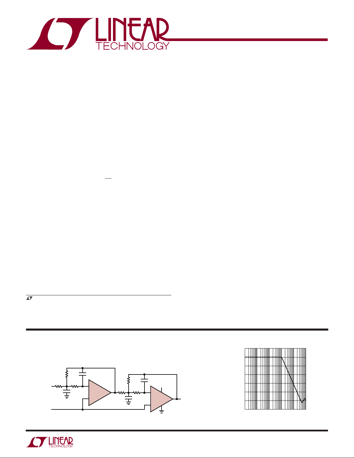
TYPICAL APPLICATIO
3V, 1MHz, 4th Order Butterworth Filter
2.67k
220pF
47pF
–
1/2 LT1801
+
VS/2
909Ω
909Ω
V
IN
U
1.1k
1.1k
2.21k
470pF
22pF
–
1/2 LT1801
+
For a single version of these amplifiers, see the LT1800
data sheet.
1MHz Filter Frequency Response
0
–20
–40
–60
3V
V
OUT
18012 TA01
GAIN (dB)
–80
–100
–120
1k 100k 1M 10M 100M
10k
FREQUENCY (Hz)
18012 TA02
18012fa
1
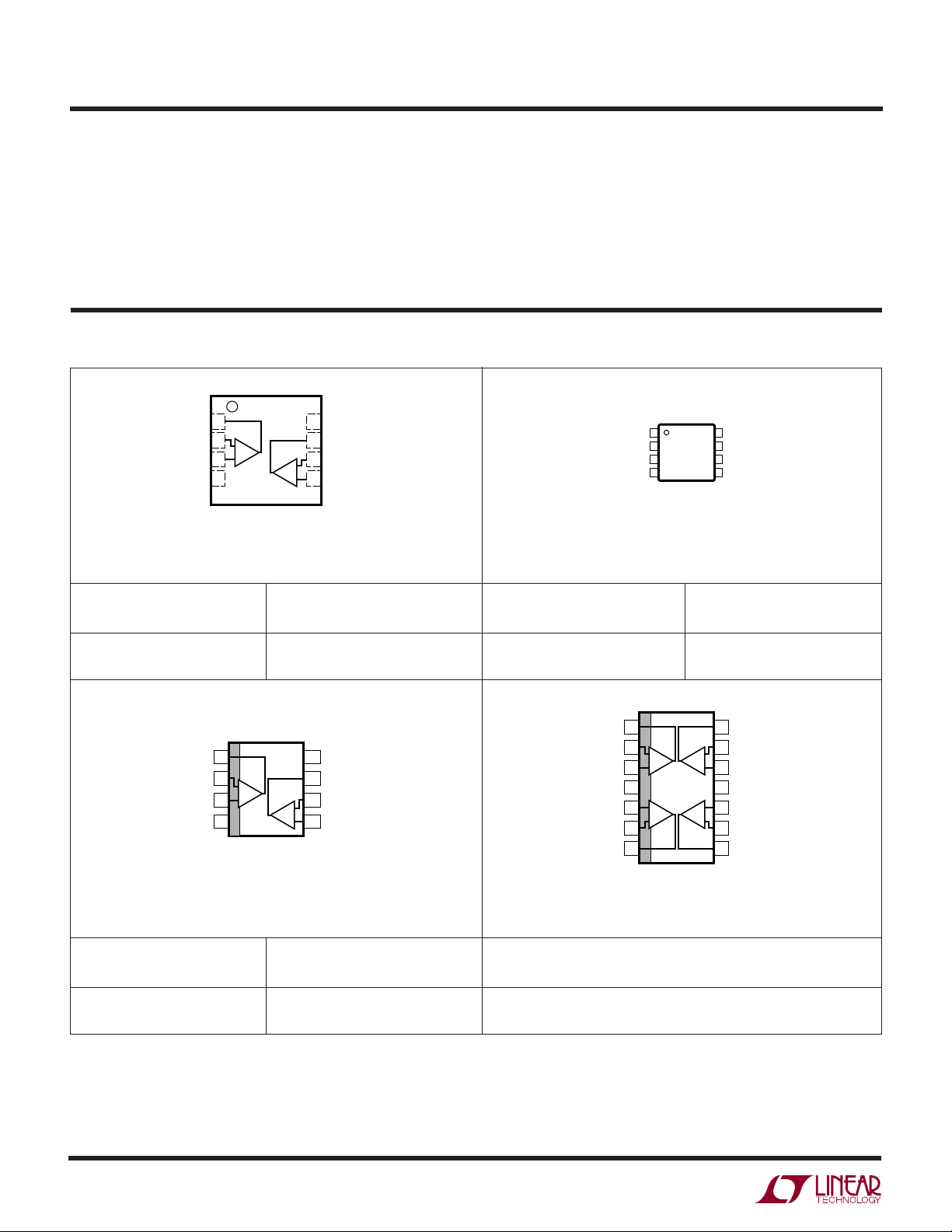
LT1801/LT1802
TOP VIEW
S PACKAGE
14-LEAD PLASTIC SO
1
2
3
4
5
6
7
14
13
12
11
10
9
8
OUT A
–IN A
+IN A
V
+
+IN B
–IN B
OUT B
OUT D
–IN D
+IN D
V
–
+IN C
–IN C
OUT C
A
BC
D
1
2
3
4
OUT A
–IN A
+IN A
V
–
8
7
6
5
V
+
OUT B
–IN B
+IN B
TOP VIEW
MS8 PACKAGE
8-LEAD PLASTIC MSOP
WWWU
ABSOLUTE AXI U RATI GS
Total Supply Voltage (V
–
S
Input Current (Note 2) ........................................ ± 10mA
Output Short-Circuit Duration (Note 3) ............ Indefinite
Operating Temperature Range (Note 4) .. – 40°C to 85°C
Specified Temperature Range (Note 5) ... –40°C to 85°C
to V
+
) ......................... 12.6V
S
(Note 1)
Junction Temperature.......................................... 150°C
Storage Temperature Range ................. –65°C to 150°C
Maximum Junction Temperature (DD Package) ... 125°C
Storage Temperature (DD Package) ..... –65°C to 125°C
Lead Temperature (Soldering, 10 sec)..................300°C
UU
W
PACKAGE/ORDER I FOR ATIO
TOP VIEW
+
8
7
6
5
8
7
6
–
+
5
V
OUT B
–IN B
+IN B
DD PART
MARKING
LAAM*
+
V
OUT B
–IN B
+IN B
–IN A
+IN A
–
V
8-LEAD (3mm × 3mm) PLASTIC DFN
T
= 125°C, θJA = 160°C/ W, (Note 10)
JMAX
ORDER PART
NUMBER
LT1801CDD
LT1801IDD
OUT A
–IN A
+IN A
–
V
1OUT A
2
3
4
DD PACKAGE
1
2
3
4
TOP VIEW
–
+
T
= 150°C, θJA = 250°C/ W, (Note 10)
JMAX
ORDER PART
NUMBER
LT1801CMS8
LT1801IMS8
MS8 PART
MARKING
LTYR
LTYS
S8 PACKAGE
8-LEAD PLASTIC SO
T
= 150°C, θJA = 190°C/ W, (Note 10)
JMAX
ORDER PART
NUMBER
LT1801CS8
LT1801IS8
Consult LTC Marketing for parts specified with wider operating temperature ranges.
*The temperature grades are identified by a label on the shipping container.
2
S8 PART
MARKING
1801
1801I
T
= 150°C, θJA = 160°C/ W, (Note 10)
JMAX
ORDER PART
NUMBER
LT1802CS
LT1802IS
18012fa

LT1801/LT1802
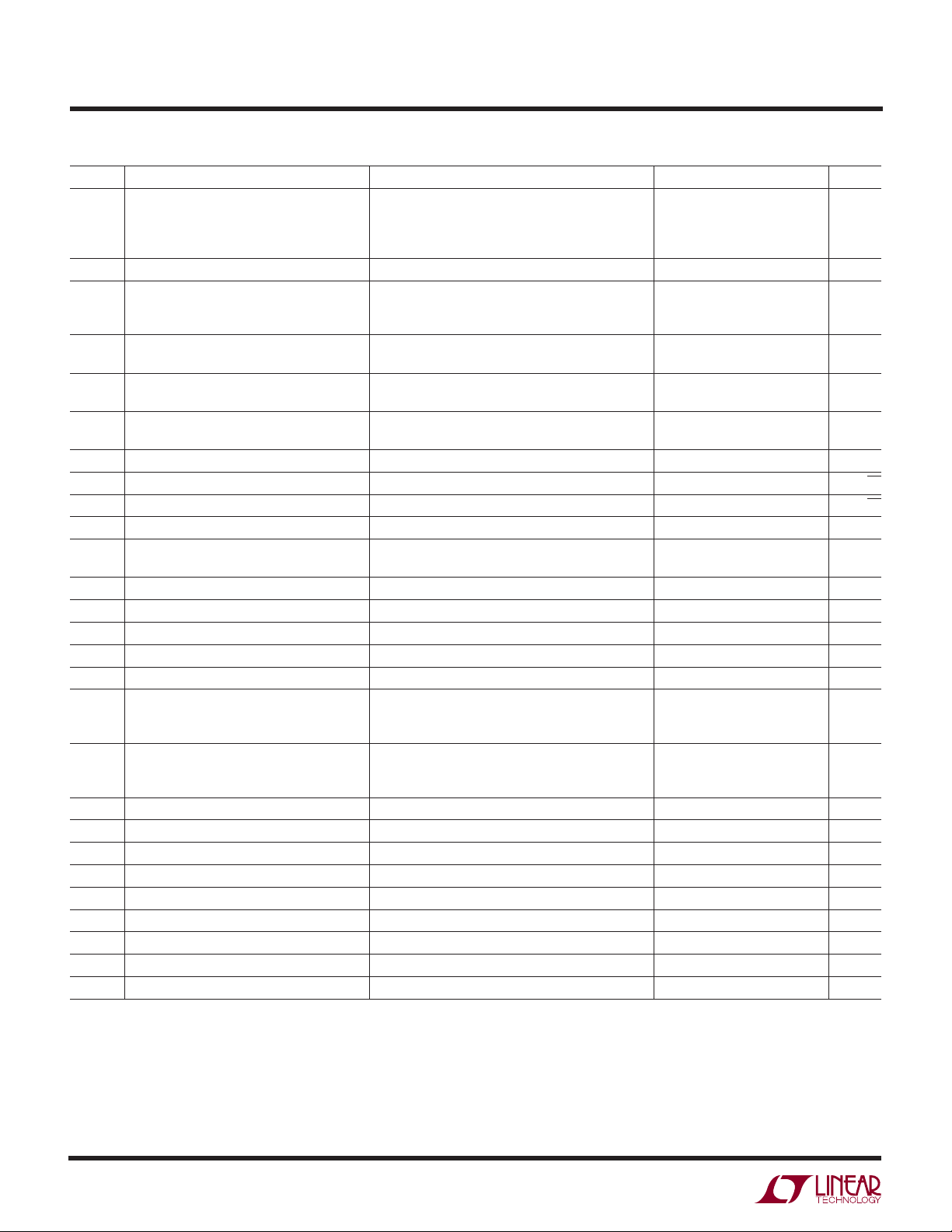
ELECTRICAL CHARACTERISTICS
TA = 25°C, VS = 5V, 0V; VS = 3V, 0V; VCM = V
SYMBOL PARAMETER CONDITIONS MIN TYP MAX UNITS
V
OS
∆V
I
B
I
OS
e
n
i
n
C
IN
A
VOL
CMRR Common Mode Rejection Ratio VS = 5V, VCM = 0V to 3.5V 85 105 dB
PSRR Power Supply Rejection Ratio VS = 2.5V to 10V, VCM = 0V 78 97 dB
V
OL
V
OH
I
SC
I
S
GBW Gain Bandwidth Product Frequency = 2MHz 40 80 MHz
SR Slew Rate VS = 5V, AV = –1, RL = 1k, VO = 4V
FPBW Full Power Bandwidth VS = 5V, AV = 1, VO = 4V
HD Harmonic Distortion VS = 5V, AV = 1, RL = 1k, VO = 2V
t
S
∆G Differential Gain (NTSC) VS = 5V, AV = 2, RL = 150Ω 0.35 %
∆θ Differential Phase (NTSC) VS = 5V, AV = 2, RL = 150Ω 0.4 Deg
Input Offset Voltage VCM = 0V 75 350 µV
Input Offset Shift VCM = 0V to VS – 1.5V 20 185 µV
OS
Input Offset Voltage Match VCM = 0V 100 650 µV
(Channel-to-Channel) (Note 9) VCM = 0V (MS8) 150 900 µV
Input Bias Current VCM = 1V 25 250 nA
Input Bias Current Match VCM = 1V 25 350 nA
(Channel-to-Channel) (Note 9) VCM = V
Input Offset Current VCM = 1V 25 200 nA
Input Noise Voltage 0.1Hz to 10Hz 1.4 µV
Input Noise Voltage Density f = 10kHz 8.5 nV/√Hz
Input Noise Current Density f = 10kHz 1 pA/√Hz
Input Capacitance 2pF
Large-Signal Voltage Gain VS = 5V, VO = 0.5V to 4.5V, RL = 1k at VS/2 35 85 V/mV
CMRR Match (Channel-to-Channel) (Note 9) VS = 5V, VCM = 0V to 3.5V 79 105 dB
Input Common Mode Range 0 V
PSRR Match (Channel-to-Channel) (Note 9) VS = 2.5V to 10V, VCM = 0V 72 97 dB
Minimum Supply Voltage (Note 6) 2.3 2.5 V
Output Voltage Swing Low (Note 7) No Load 16 60 mV
Output Voltage Swing High (Note 7) No Load 18 60 mV
Short-Circuit Current VS = 5V 20 45 mA
Supply Current per Amplifier 1.6 2 mA
Settling Time 0.01%, VS = 5V, V
= half supply, unless otherwise noted.
OUT
VCM = 0V (MS8) 140 500 µV
VCM = 0V (DD) 175 800 µV
= V
V
CM
S
VCM = 0V (DD) 280 1200 µV
V
= V
CM
S
S
VCM = V
S
= 5V, VO = 1V to 4V, RL = 100Ω at VS/2 3.5 8 V/mV
V
S
= 3V, VO = 0.5V to 2.5V, RL = 1k at VS/2 30 85 V/mV
V
S
VS = 3V, VCM = 0V to 1.5V 78 97 dB
= 3V, VCM = 0V to 1.5V 72 97 dB
V
S
= 5mA 85 200 mV
I
SINK
= 20mA 225 500 mV
I
SINK
I
= 5mA 120 250 mV
SOURCE
= 20mA 450 800 mV
I
SOURCE
VS = 3V 20 40 mA
P-P
= 2V, AV = 1, RL = 1k 250 ns
STEP
0.5 3 mV
500 1500 nA
25 500 nA
25 200 nA
S
P-P
12.5 25 V/µs
2 MHz
, fC = 500kHz –75 dBc
P-P
P-P
V
18012fa
3
LT1801/LT1802
ELECTRICAL CHARACTERISTICS
0°C < TA < 70°C. VS = 5V, 0V; VS = 3V, 0V; VCM = V
OUT
The ● denotes the specifications which apply over the temperature range of
= half supply, unless otherwise noted.
SYMBOL PARAMETER CONDITIONS MIN TYP MAX UNITS
V
∆V
OS
Input Offset Voltage VCM = 0V ● 125 500 µV
= 0V (MS8) ● 140 650 µV
V
CM
= 0V (DD) ● 290 950 µV
V
CM
VCM = V
S
Input Offset Shift VCM = 0V to VS – 1.5V ● 30 275 µV
OS
● 0.6 3.5 mV
Input Offset Voltage Match VCM = 0V ● 200 850 µV
(Channel-to-Channel) (Note 9) V
= 0V (MS8) ● 200 1250 µV
CM
VCM = 0V (DD) ● 275 1500 µV
VOS TC Input Offset Voltage Drift (Note 8) ● 1.5 5 µV/°C
I
B
Input Bias Current VCM = 1V ● 50 300 nA
VCM = VS – 0.2V ● 550 2000 nA
Input Bias Current Match VCM = 1V ● 25 400 nA
(Channel-to-Channel) (Note 9) V
I
OS
Input Offset Current VCM = 1V ● 25 300 nA
= VS – 0.2V ● 25 600 nA
CM
VCM = VS – 0.2V ● 25 300 nA
A
VOL
Large-Signal Voltage Gain VS = 5V, VO = 0.5V to 4.5V, RL = 1k at VS/2 ● 25 75 V/mV
= 5V, VO = 1V to 4V, RL = 100Ω at VS/2 ● 2.5 6 V/mV
V
S
VS = 3V, VO = 0.5V to 2.5V, RL = 1k at VS/2 ● 20 75 V/mV
CMRR Common Mode Rejection Ratio VS = 5V, VCM = 0V to 3.5V ● 82 101 dB
= 3V, VCM = 0V to 1.5V ● 74 93 dB
V
S
CMRR Match (Channel-to-Channel) (Note 9) VS = 5V, VCM = 0V to 3.5V ● 76 101 dB
= 3V, VCM = 0V to 1.5V ● 68 93 dB
V
S
Input Common Mode Range ● 0V
S
PSRR Power Supply Rejection Ratio VS = 2.5V to 10V, VCM = 0V ● 74 91 dB
PSRR Match (Channel-to-Channel) (Note 9) VS = 2.5V to 10V, VCM = 0V ● 68 91 dB
Minimum Supply Voltage (Note 6) ● 2.3 2.5 V
V
OL
V
OH
I
SC
I
S
Output Voltage Swing Low (Note 7) No Load ● 18 80 mV
= 5mA ● 100 225 mV
I
SINK
I
= 20mA ● 300 600 mV
SINK
Output Voltage Swing High (Note 7) No Load ● 25 80 mV
= 5mA ● 150 300 mV
I
SOURCE
I
= 20mA ● 600 950 mV
SOURCE
Short-Circuit Current VS = 5V ● 20 40 mA
= 3V ● 15 30 mA
V
S
Supply Current per Amplifier ● 2 2.8 mA
GBW Gain Bandwidth Product Frequency = 2MHz ● 35 75 MHz
SR Slew Rate VS = 5V, AV = –1, RL = 1k, VO = 4V
P-P
● 11 22 V/µs
V
4
18012fa
LT1801/LT1802
ELECTRICAL CHARACTERISTICS
–40° C < T
< 85°C. VS = 5V, 0V; VS = 3V, 0V; VCM = V
A
The ● denotes the specifications which apply over the temperature range of
= half supply, unless otherwise noted. (Note 5)
OUT
SYMBOL PARAMETER CONDITIONS MIN TYP MAX UNITS
V
OS
Input Offset Voltage VCM = 0V ● 175 700 µV
VCM = 0V (MS8) ● 200 850 µV
V
= 0V (DD) ● 320 1150 µV
CM
∆V
VCM = V
S
Input Offset Shift VCM = 0V to VS – 1.5V ● 30 300 µV
OS
● 0.75 4 mV
Input Offset Voltage Match VCM = 0V ● 200 1250 µV
(Channel-to-Channel) (Note 9) VCM = 0V (MS8) ● 280 1600 µV
V
= 0V (DD) ● 320 1800 µV
CM
VOS TC Input Offset Voltage Drift (Note 8) ● 1.5 5 µV/°C
I
B
Input Bias Current ● 50 400 nA
V
= VS – 0.2V ● 600 2250 nA
CM
Input Bias Current Match VCM = 1V ● 25 450 nA
(Channel-to-Channel) (Note 9) V
I
OS
A
VOL
Input Offset Current VCM = 1V ● 25 350 nA
Large-Signal Voltage Gain VS = 5V, VO = 0.5V to 4.5V, RL = 1k at VS/2 ● 20 65 V/mV
= VS – 0.2V ● 25 700 nA
CM
V
= VS – 0.2V ● 25 350 nA
CM
VS = 5V, VO = 1.5V to 3.5V, RL = 100Ω at VS/2 ● 2 6 V/mV
V
= 3V, VO = 0.5V to 2.5V, RL = 1k at VS/2 ● 17.5 65 V/mV
S
CMRR Common Mode Rejection Ratio VS = 5V, VCM = 0V to 3.5V ● 81 101 dB
V
= 3V, VCM = 0V to 1.5V ● 73 93 dB
S
CMRR Match (Channel-to-Channel) (Note 9) VS = 5V, VCM = 0V to 3.5V ● 75 101 dB
V
= 3V, VCM = 0V to 1.5V ● 67 93 dB
S
Input Common Mode Range ● 0V
S
PSRR Power Supply Rejection Ratio VS = 2.5V to 10V, VCM = 0V ● 73 90 dB
PSRR Match (Channel-to-Channel) (Note 9) VS = 2.5V to 10V, VCM = 0V ● 67 90 dB
Minimum Supply Voltage (Note 6) VCM = VO = 0.5V ● 2.3 2.5 V
V
OL
V
OH
I
SC
I
S
Output Voltage Swing Low (Note 7) No Load ● 15 90 mV
I
= 5mA ● 105 250 mV
SINK
I
= 10mA ● 170 400 mV
SINK
Output Voltage Swing High (Note 7) No Load ● 25 90 mV
I
= 5mA ● 150 350 mV
SOURCE
I
= 10mA ● 300 700 mV
SOURCE
Short-Circuit Current VS = 5V ● 12.5 30 mA
V
= 3V ● 12.5 30 mA
S
Supply Current per Amplifier ● 2.1 3 mA
GBW Gain Bandwidth Product Frequency = 2MHz ● 25 70 MHz
SR Slew Rate VS = 5V, AV = –1, RL = 1k, VO = 4V ● 918 V/µs
V
18012fa
5
LT1801/LT1802
ELECTRICAL CHARACTERISTICS
TA = 25°C, VS = ± 5V, VCM = 0V, V
= 0V, unless otherwise noted.
OUT
SYMBOL PARAMETER CONDITIONS MIN TYP MAX UNITS
V
OS
Input Offset Voltage VCM = V
V
V
V
∆V
Input Offset Shift VCM = V
OS
Input Offset Voltage Match VCM = V
(Channel-to-Channel) (Note 9) V
V
I
B
Input Bias Current VCM = V
V
Input Bias Current Match VCM = V
(Channel-to-Channel) (Note 9) V
I
OS
Input Offset Current VCM = V
V
Input Noise Voltage 0.1Hz to 10Hz 1.4 µV
e
n
i
n
C
IN
A
VOL
Input Noise Voltage Density f = 10kHz 8.5 nV/√Hz
Input Noise Current Density f = 10kHz 1 pA/√Hz
Input Capacitance f = 100kHz 2 pF
Large-Signal Voltage Gain VO = –4V to 4V, RL = 1k 25 70 V/mV
V
CMRR Common Mode Rejection Ratio VCM = V
CMRR Match (Channel-to-Channel) (Note 9) VCM = V
Input Common Mode Range V
PSRR Power Supply Rejection Ratio V
PSRR Match (Channel-to-Channel) (Note 9) V
V
OL
Output Voltage Swing Low (Note 7) No Load 15 70 mV
I
I
V
OH
Output Voltage Swing High (Note 7) No Load 20 80 mV
I
I
I
SC
I
S
Short-Circuit Current 25 50 mA
Supply Current per Amplifier 1.8 3 mA
–
S
–
= V
(MS8) 180 750 µV
CM
S
–
= V
(DD) 260 1050 µV
CM
S
+
= V
CM
S
–
+
to V
– 1.5V 30 475 µV
S
S
–
S
–
= V
(MS8) 275 1300 µV
CM
S
–
= V
(DD) 325 1600 µV
CM
S
–
+ 1V 25 250 nA
S
+
= V
CM
S
–
+ 1V 20 350 nA
S
+
= V
CM
S
–
+ 1V 20 250 nA
S
+
= V
CM
S
= –2V to 2V, RL = 100Ω 2.5 7 V/mV
O
–
to 3.5V 85 109 dB
S
–
to 3.5V 79 109 dB
S
+
= 2.5V to 10V, V
S
+
= 2.5V to 10V, V
S
= 5mA 90 200 mV
SINK
= 20mA 225 500 mV
SINK
= 5mA 130 260 mV
SOURCE
= 20mA 450 850 mV
SOURCE
–
= 0V 78 97 dB
S
–
= 0V 72 97 dB
S
S
150 600 µV
0.7 3.5 mV
150 1000 µV
400 1500 nA
20 500 nA
20 250 nA
–
+
V
S
P-P
GBW Gain Bandwidth Product Frequency = 2MHz 70 MHz
FPBW Full Power Bandwidth VO = 8V
P-P
0.9 MHz
SR Slew Rate AV = – 1, RL = 1k, VO = ± 4V, Measured at VO = ±2V 20 V/µs
HD Harmonic Distortion AV = 1, RL = 1k, VO = 2V
t
S
Settling Time 0.01%, V
= 5V, AV = 1V, RL = 1k 300 ns
STEP
, fC = 500kHz –75 dBc
P-P
∆G Differential Gain (NTSC) AV = 2, RL = 150Ω 0.35 %
∆θ Differential Phase (NTSC) AV = 2, RL = 150Ω 0.2 Deg
V
6
18012fa

LT1801/LT1802
ELECTRICAL CHARACTERISTICS
0°C < TA < 70°C. VS = ± 5V, VCM = 0V, V
= 0V, unless otherwise noted.
OUT
The ● denotes the specifications which apply over the temperature range of
SYMBOL PARAMETER CONDITIONS MIN TYP MAX UNITS
V
∆V
OS
Input Offset Voltage VCM = V
Input Offset Shift VCM = V
OS
Input Offset Voltage Match VCM = V
(Channel-to-Channel) (Note 9) V
V
V
V
V
–
S
–
= V
(MS8) ● 220 1000 µV
CM
S
–
= V
(DD) ● 290 1300 µV
CM
S
+
= V
CM
S
–
+
to V
– 1.5V ● 45 675 µV
S
S
–
S
–
= V
(MS8) ● 300 1700 µV
CM
S
–
= V
(DD) ● 340 1950 µV
CM
S
● 200 800 µV
● 0.75 4 mV
● 240 1500 µV
VOS TC Input Offset Voltage Drift (Note 8) ● 1.5 5 µV/°C
I
B
Input Bias Current VCM = V
V
Input Bias Current Match VCM = V
(Channel-to-Channel) (Note 9) V
I
OS
Input Offset Current VCM = V
V
A
VOL
Large-Signal Voltage Gain VO = –4V to 4V, RL = 1k ● 15 55 V/mV
V
CMRR Common Mode Rejection Ratio VCM = V
CMRR Match (Channel-to-Channel) (Note 9) VCM = V
Input Common Mode Range ● V
PSRR Power Supply Rejection Ratio V
PSRR Match (Channel-to-Channel) (Note 9) V
V
OL
Output Voltage Swing Low (Note 7) No Load ● 17 80 mV
I
I
V
OH
Output Voltage Swing High (Note 7) No Load ● 25 90 mV
I
I
I
SC
I
S
Short-Circuit Current ● 22.5 45 mA
Supply Current per Amplifier ● 2.4 4 mA
–
+ 1V ● 30 300 nA
S
+
= V
– 0.2V ● 450 2000 nA
CM
S
–
+ 1V ● 25 400 nA
S
+
= V
– 0.2V ● 25 700 nA
CM
S
–
+ 1V ● 25 300 nA
S
+
= V
– 0.2V ● 25 300 nA
CM
S
= –2V to 2V, RL = 100Ω ● 2 5 V/mV
O
–
to 3.5V ● 82 105 dB
S
–
to 3.5V ● 76 105 dB
S
+
= 2.5V to 10V, V
S
+
= 2.5V to 10V, V
S
= 5mA ● 105 250 mV
SINK
= 20mA ● 250 575 mV
SINK
= 5mA ● 150 310 mV
SOURCE
= 20mA ● 600 975 mV
SOURCE
–
= 0V ● 74 91 dB
S
–
= 0V ● 68 93 dB
S
–
S
+
V
S
GBW Gain Bandwidth Product Frequency = 2MHz ● 70 MHz
SR Slew Rate AV = – 1, RL = 1k, VO = ± 4V, ● 20 V/µs
Measured at V
= ±2V
O
V
The ● denotes the specifications which apply over the temperature range of –40°C < TA < 85°C. VS = ±5V, VCM = 0V, V
= 0V, unless
OUT
otherwise noted. (Note 5)
SYMBOL PARAMETER CONDITIONS MIN TYP MAX UNITS
V
∆V
OS
Input Offset Voltage VCM = V
Input Offset Shift VCM = V
OS
Input Offset Voltage Match VCM = V
(Channel-to-Channel) (Note 9) V
V
V
V
V
–
S
–
= V
(MS8) ● 350 1200 µV
CM
S
–
= V
(DD) ● 350 1500 µV
CM
S
+
= V
CM
S
–
+
to V
– 1.5V ● 50 750 µV
S
S
–
S
–
= V
(MS8) ● 380 1900 µV
CM
S
–
= V
(DD) ● 410 2100 µV
CM
S
● 350 1000 µV
● 0.75 5 mV
● 280 1700 µV
18012fa
7

LT1801/LT1802
ELECTRICAL CHARACTERISTICS
of – 40°C < T
< 85°C. VS = ± 5V, VCM = 0V, V
A
= 0V, unless otherwise noted. (Note 5)
OUT
The ● denotes the specifications which apply over the temperature range
SYMBOL PARAMETER CONDITIONS MIN TYP MAX UNITS
VOS TC Input Offset Voltage Drift (Note 8) ● 1.5 5 µV/°C
I
B
Input Bias Current VCM = V
V
Input Bias Current Match VCM = V
(Channel-to-Channel) (Note 9) V
I
OS
Input Offset Current VCM = V
V
A
VOL
Large-Signal Voltage Gain VO = –4V to 4V, RL = 1k ● 12.5 55 V/mV
V
CMRR Common Mode Rejection Ratio VCM = V
CMRR Match (Channel-to-Channel) (Note 9) VCM = V
Input Common Mode Range ● V
PSRR Power Supply Rejection Ratio V
PSRR Match (Channel-to-Channel) (Note 9) V
V
OL
Output Voltage Swing Low (Note 7) No Load ● 20 100 mV
I
I
V
OH
Output Voltage Swing High (Note 7) No Load ● 30 110 mV
I
I
I
SC
I
S
Short-Circuit Current ● 12.5 30 mA
Supply Current per Amplifier ● 2.6 4.5 mA
–
+ 1V ● 50 400 nA
S
+
= V
– 0.2V ● 450 2250 nA
CM
S
–
+ 1V ● 25 450 nA
S
+
= V
– 0.2V ● 25 700 nA
CM
S
–
+ 1V ● 25 350 nA
S
+
= V
– 0.2V ● 25 350 nA
CM
S
= –1V to 1V, RL = 100Ω ● 2 5 V/mV
O
–
to 3.5V ● 81 104 dB
S
–
to 3.5V ● 75 104 dB
S
+
= 2.5V to 10V, V
S
+
= 2.5V to 10V, V
S
= 5mA ● 110 275 mV
SINK
= 10mA ● 180 400 mV
SINK
= 5mA ● 150 350 mV
SOURCE
= 10mA ● 300 700 mV
SOURCE
–
= 0V ● 73 90 dB
S
–
= 0V ● 67 90 dB
S
–
S
+
V
S
GBW Gain Bandwidth Product Frequency = 2MHz ● 65 MHz
SR Slew Rate AV = – 1, RL = 1k, VO = ± 4V, ● 15 V/µs
Measured at V
Note 1: Absolute Maximum Ratings are those values beyond which the life
of the device may be impaired.
Note 2: The inputs are protected by back-to-back diodes. If the differential
input voltage exceeds 1.4V, the input current should be limited to less than
10mA.
Note 3: A heat sink may be required to keep the junction temperature
below the absolute maximum rating when the output is shorted
indefinitely.
Note 4: The LT1801C/LT1801I and LT1802C/LT1802I are guaranteed
functional over the temperature range of – 40°C to 85°C.
Note 5: The LT1801C/LT1802C are guaranteed to meet specified
performance from 0°C to 70°C. The LT1801C/LT1802C are designed,
characterized and expected to meet specified performance from
–40°C to 85°C but are not tested or QA sampled at these temperatures.
= ±2V
O
Note 6: Minimum supply voltage is guaranteed by power supply rejection
ratio test.
Note 7: Output voltage swings are measured between the output and
power supply rails.
Note 8: This parameter is not 100% tested.
Note 9: Matching parameters are the difference between amplifiers A
and D and between B and C on the LT1802; between the two amplifiers
on the LT1801.
Note 10: Thermal resistance (θ
) varies with the amount of PC board
JA
metal connected to the package. The specified values are for short traces
connected to the leads. If desired, the thermal resistance can be
substantially reduced by connecting Pin 4 of the SO-8 and MS8, Pin 11 of
the SO-14 or the underside metal of the DD package to a larger metal area
–
trace).
(V
S
The LT1801I/LT1802I are guaranteed to meet specified performance from
–40°C to 85°C.
V
8
18012fa

UW
TEMPERATURE (°C)
–60
–0.1
INPUT BIAS (µA)
0
0.2
0.3
0.4
40 60 80
0.8
18012 G06
0.1
–40 –20 0 20
0.5
0.6
0.7
NPN ACTIVE
V
S
= 5V, 0V
V
CM
= 5V
PNP ACTIVE
V
S
= 5V, 0V
V
CM
= 1V
TYPICAL PERFOR A CE CHARACTERISTICS
LT1801/LT1802
VOS Distribution, VCM = 0V
(PNP Stage)
35
VS = 5V, 0V
= 0V
V
CM
30
25
20
15
10
PERCENT OF UNITS (%)
5
0
–150 –50 250
–250
INPUT OFFSET VOLTAGE (µV)
50 150
Offset Voltage
vs Input Common Mode Voltage
500
TA = –55°C
TA = 25°C
TA = 125°C
1
INPUT COMMON MODE VOLTAGE (V)
3
2
–100
–200
OFFSET VOLTAGE (µV)
–300
–400
–500
400
300
200
100
0
0
18012 G01
VS = 5V, 0V
TYPICAL PART
4
18012 G04
VOS Distribution, VCM = 5V
(NPN Stage)
45
VS = 5V, 0V
= 5V
V
40
CM
35
30
25
20
15
PERCENT OF UNITS (%)
10
5
0
–1200 –400 2000
–2000
INPUT OFFSET VOLTAGE (µV)
400 1200
18012 G02
Input Bias Current
vs Common Mode Voltage
1.0
VS = 5V, 0V
= 25°C
0.8
0.6
0.4
0.2
–0.2
–0.4
INPUT BIAS CURRENT (µA)
–0.6
–0.8
5
–1.0
T
A
= 125°C
T
A
= –55°C
T
A
0
0
–1
INPUT COMMON MODE VOLTAGE (V)
1
23
4
5
18012 G05
6
Supply Current vs Supply Voltage
4
PER AMPLIFIER
3
2
SUPPLY CURRENT (mA)
1
0
3579102468 11
10
TOTAL SUPPLY VOLTAGE (V)
TA = 125°C
TA = 25°C
TA = –55°C
Input Bias Current
vs Temperature
12
18012 G03
Output Saturation Voltage
vs Load Current (Output Low)
10
VS = 5V, 0V
1
0.1
TA = 125°C
0.01
TA = –55°C
OUTPUT SATURATION VOLTAGE (V)
0.001
0.01 0.1
TA = 25°C
LOAD CURRENT (mA)
1 10 100
18012 G07
Output Saturation Voltage
vs Load Current (Output High)
10
VS = 5V, 0V
1
0.1
TA = 125°C
0.01
TA = –55°C
OUTPUT SATURATION VOLTAGE (V)
0.001
0.01 0.1
TA = 25°C
1 10 100
LOAD CURRENT (mA)
18012 G08
18012fa
9

LT1801/LT1802
OUTPUT VOLTAGE (V)
0
–2000
CHANGE IN OFFSET VOLTAGE (µV)
–1200
–400
400
0.5
1
1.5 2
18012 G11
2.5
1200
2000
–1600
–800
0
800
1600
3
VS = 3V, 0V
R
L
TO GND
RL = 1k
RL = 100Ω
FREQUENCY (kHz)
20
NOISE VOLTAGE (nV/√Hz)
40
60
10
30
50
0.01 1 10 100
18012 G16
0
0.1
VS = 5V, 0V
NPN ACTIVE
V
CM
= 4.25V
PNP ACTIVE
V
CM
= 2.5V
UW
TYPICAL PERFOR A CE CHARACTERISTICS
Output Short-Circuit Current
Minimum Supply Voltage
0.6
0.4
0.2
0
–0.2
–0.4
CHANGE IN OFFSET VOLTAGE (mV)
–0.6
1.5 2.5
0
TA = –55°C
TA = 25°C
TA = 125°C
2
TOTAL SUPPLY VOLTAGE (V)
3.5 5.5
3
4.5
5
4
18012 G09
vs Power Supply Voltage
70
60
50
40
30
20
10
0
–10
–20
–30
–40
–50
OUTPUT SHORT-CIRCUIT CURRENT (mA)
–60
–70
1.5
TA = 25°C
TA = 125°C
TA = –55°C SINKING
TA = 125°C
TA = 25°C
2.5
2
POWER SUPPLY VOLTAGE (±V)
3.5 5
3
SOURCINGTA = –55°C
4
Open-Loop Gain
4.5
18012 G10
Open-Loop Gain
2000
1600
1200
800
400
0
–400
–800
–1200
CHANGE IN OFFSET VOLTAGE (µV)
–1600
–2000
10
0
10.5
21.5
OUTPUT VOLTAGE (V)
120
110
100
90
80
70
OFFSET VOLTAGE (µV)
60
50
40
VS = 5V, 0V
TO GND
R
L
RL = 1k
RL = 100Ω
3 3.5 4.5
4
2.5
5
18012 G12
Warm-Up Drift vs Time
VS = ±5V
VS = ±2.5V
VS = ±1.5V
20 40 80
0
TIME AFTER POWER-UP (SECONDS)
60
Open-Loop Gain Offset Voltage vs Output Current
2000
1600
1200
800
400
–400
–800
–1200
CHANGE IN OFFSET VOLTAGE (µV)
–1600
–2000
VS = ±5V
TO GND
R
L
0
–3–4
–5
–1–2
OUTPUT VOLTAGE (V)
RL = 1k
RL = 100Ω
12 4
0
3
5
18012 G13
2.0
VS = ±5V
1.5
1.0
0.5
0
–0.5
TA = 25°C
–1.0
CHANGE IN OFFSET VOLTAGE (mV)
–1.5
–2.0
–45
–60
TA = –55°C
TA = 125°C
–15
0
–30
OUTPUT CURRENT (mA)
Input Noise Voltage vs Frequency
TYPICAL PART
100 120 140
18012 G15
15
30
45
18012 G14
18012fa
60

UW
FREQUENCY (MHz)
0.01
10
OPEN-LOOP GAIN (dB)
PHASE (DEG)
20
30
40
50
0.1 1 10 100 300
18012 G22
0–40
–10
–20
–30
60
70
–20
0
20
40
60
–60
–80
–100
80
100
VS = ±2.5V
V
S
= ±5V
PHASE
GAIN
TYPICAL PERFOR A CE CHARACTERISTICS
Input Current Noise vs Frequency
3.0
2.5
2.0
= 4.25V
CM
PNP ACTIVE
= 2.5V
V
CM
0.1
FREQUENCY (kHz)
1.5
1.0
NOISE CURRENT (pA/√Hz)
NPN ACTIVE
0.5
V
0
0.01 1 10 100
VS = 5V, 0V
Gain Bandwidth and Phase
Margin vs Temperature
100
90
80
70
60
50
GAIN BANDWIDTH (MHz)
–35 5
–55
GBW PRODUCT
PHASE MARGIN
V
PHASE MARGIN
V
–15
TEMPERATURE (°C)
GBW PRODUCT
V
S
= ±5V
V
S
= ±2.5V
S
= ±5V
S
45 125
65
25
= ±2.5V
85
18012 G17
105
18012 G20
PHASE MARGIN (DEG)
60
50
40
30
20
10
0.1Hz to 10Hz Input Voltage Noise
2000
VS = 5V, 0V
1000
0
–1000
INPUT NOISE VOLTAGE (nV)
–2000
0
246 107135 9
TIME (SECONDS)
Slew Rate vs Temperature
35
AV = –1
= RG = 1k
R
SLEW RATE (V/µs)
30
25
20
15
10
–55
F
= 1k
R
L
–35 5
–15
VS = ±2.5V
= ±5V
V
S
45 125
25
TEMPERATURE (°C)
8
85
65
18012 G18
105
18012 G21
LT1801/LT1802
Gain Bandwidth and Phase
Margin vs Supply Voltage
100
90
GAIN BANDWIDTH
80
70
60 60
GAIN BANDWIDTH (MHz)
0
PRODUCT
PHASE MARGIN
246 107135 9
TOTAL SUPPLY VOLTAGE (V)
Gain and Phase vs Frequency
TA = 25°C
8
18012 G19
PHASE MARGIN (DEG)
50
40
30
20
Gain vs Frequency (AV = 1)
12
RL = 1k
= 10pF
C
L
9
= 1
A
V
6
3
0
GAIN (dB)
–3
–6
–9
–12
0.1 10 100 300
1
FREQUENCY (MHz)
VS = ±2.5V
VS = ±5V
18012 G23
Gain vs Frequency (AV = 2)
18
RL = 1k
= 10pF
C
L
15
= 2
A
V
12
9
6
GAIN (dB)
3
0
–3
–6
0.1 10 100 300
VS = ±5V
1
FREQUENCY (MHz)
VS = ±2.5V
18012 G24
18012fa
11

LT1801/LT1802
UW
TYPICAL PERFOR A CE CHARACTERISTICS
Output Impedance vs Frequency
600
VS = ±2.5V
100
AV = 10
AV = 1
AV = 2
1 10 100 500
FREQUENCY (MHz)
0.1
OUTPUT IMPEDANCE (Ω)
0.01
0.001
10
1
0.1
Series Output Resistor
vs Capacitive Load
60
VS = 5V, 0V
55
= 1
A
V
50
45
40
35
30
25
OVERSHOOT (%)
20
15
10
ROS = RL = 50Ω
5
0
10
ROS = 20Ω
100 1000 10000
CAPACITIVE LOAD (pF)
ROS = 10Ω
18012 G25
18012 G28
Common Mode Rejection Ratio
vs Frequency
120
VS = 5V, 0V
100
80
60
40
20
COMMON MODE REJECTION RATIO (dB)
0
0.01 1 10 100
0.1
FREQUENCY (MHz)
Series Output Resistor
vs Capacitive Load
60
VS = 5V, 0V
55
= 2
A
V
50
45
40
35
30
25
OVERSHOOT (%)
20
15
10
5
ROS = RL = 50Ω
0
10
100 1000 10000
CAPACITIVE LOAD (pF)
ROS = 10Ω
ROS = 20Ω
18012 G26
18012 G29
Power Supply Rejection Ratio
vs Frequency
90
80
70
NEGATIVE
60
SUPPLY
50
40
30
20
10
0
POWER SUPPLY REJECTION RATIO (dB)
–10
0.001
0.01 0.1 1 10 100
FREQUENCY (MHz)
POSITIVE
SUPPLY
Distortion vs Frequency
–40
VS = 5V, 0V
= 1
A
V
–50
–60
–70
–80
DISTORTION (dBc)
–90
–100
–110
0.01
V
OUT
= 2V
P-P
RL = 150Ω, 2ND
RL = 1k, 3RD
0.1 1 10
FREQUENCY (MHz)
RL = 150Ω, 3RD
VS = 5V, 0V
= 25°C
T
A
18012 G27
RL = 1k, 2ND
18012 G30
12
Distortion vs Frequency
–40
VS = 5V, 0V
= 2
A
V
–50
–60
–70
–80
DISTORTION (dBc)
–90
–100
–110
V
0.01
= 2V
OUT
P-P
RL = 150Ω, 2ND
RL = 1k, 3RD
0.1 1 10
FREQUENCY (MHz)
RL = 1k,
2ND
RL = 150Ω,
3RD
18012 G31
Maximum Undistorted Output
Signal vs Frequency
4.6
4.5
)
P-P
4.4
4.3
4.2
4.1
OUTPUT VOLTAGE SWING (V
4.0
VS = 5V, 0V
= 1k
R
L
3.9
1k 100k 1M 10M
10k
FREQUENCY (Hz)
AV = 2
AV = –1
18012 G32
18012fa

UW
TYPICAL PERFOR A CE CHARACTERISTICS
LT1801/LT1802
5V Large-Signal Response
1V/DIV
0V
= 5V, 0V 100ns/DIV 18012 G33
V
S
AV = 1
= 1k
R
L
± 5V Large-Signal Response
2V/DIV
0V
50mV/DIV
0V
50mV/DIV
0V
5V Small-Signal Response
= 5V, 0V 50ns/DIV 18012 G34
V
S
AV = 1
= 1k
R
L
±5V Small-Signal Response
= ±5V 200ns/DIV 18012 G35
V
S
AV = 1
= 1k
R
L
V
IN
1V/DIV
0V
V
OUT
2V/DIV
= ±5V 50ns/DIV 18012 G36
V
S
AV = 1
= 1k
R
L
Output Overdriven Recovery
VS = 5V, 0V 100ns/DIV 18012 G37
AV = 2
R
= 1k
L
18012fa
13

LT1801/LT1802
WUUU
APPLICATIO S I FOR ATIO
Circuit Description
The LT1801/LT1802 have an input and output signal range
that covers from the negative power supply to the positive
power supply. Figure 1 depicts a simplified schematic of
the amplifier. The input stage is comprised of two differential amplifiers, a PNP stage Q1/Q2 and an NPN stage Q3/
Q4 that are active over the different ranges of common
mode input voltage. The PNP differential pair is active
between the negative supply to approximately 1.2V below
the positive supply. As the input voltage moves closer
toward the positive supply, the transistor Q5 will steer the
tail current I1 to the current mirror Q6/Q7, activating the
NPN differential pair and the PNP pair becomes inactive
for the rest of the input common mode range up to the
positive supply. Also at the input stage, devices Q17 to
Q19 act to cancel the bias current of the PNP input pair.
When Q1-Q2 are active, the current in Q16 is controlled to
be the same as the current in Q1-Q2, thus the base current
of Q16 is nominally equal to the base current of the input
devices. The base current of Q16 is then mirrored by
devices Q17-Q19 to cancel the base current of the input
devices Q1-Q2.
A pair of complementary common emitter stages Q14/
Q15 that enable the output to swing from rail to rail
constructs the output stage. The capacitors C2 and C3
form the local feedback loops that lower the output impedance at high frequency. These devices are fabricated on
Linear Technology’s proprietary high speed complementary bipolar process.
Power Dissipation
The LT1801 amplifier is offered in a small package, SO-8,
which has a thermal resistance of 190°C/W, θJA. So there
is a need to ensure that the die’s junction temperature
should not exceed 150°C. Junction temperature TJ is
calculated from the ambient temperature TA, power dissipation PD and thermal resistance θJA:
TJ = TA + (PD • θJA)
The power dissipation in the IC is the function of the supply
voltage, output voltage and the load resistance. For a given
supply voltage, the worst-case power dissipation P
DMAX
occurs at the maximum supply current and the output
+
V
R3 R4 R5
–
+
V
V
+
I
2
+IN
–IN
Q16
Q18Q17
–
V
ESDD2ESDD1
D6D7D8
D5
ESDD3ESDD4
–
V+V
Q19
D1
D2
Q4
Q7
Q5 V
Q3
+
I
1
BIAS
Q2
Q1
D3
D4
Q6
Q10
Q11
Q12
Q13 Q15
C2
+
I
3
C
C
–
V
BUFFER
AND
OUTPUT BIAS
Q9
Q8
C1
R2R1
OUT
Q14
18012 F01
Figure 1. LT1801/LT1802 Simplified Schematic Diagram
14
18012fa

WUUU
APPLICATIO S I FOR ATIO
LT1801/LT1802
voltage is at half of either supply voltage (or the maximum
swing is less than 1/2 supply voltage). P
= (VS • I
P
DMAX
Example: An LT1801 in an SO-8 package operating on ±5V
supplies and driving a 50Ω load, the worst-case power
dissipation is given by:
P
If both amplifiers are loaded simultaneously, then the total
power dissipation is 0.34W.
The maximum ambient temperature that the part is allowed to operate is:
TA = TJ – (P
= 150°C – (0.34W • 190°C/W) = 85°C
Input Offset Voltage
The offset voltage will change depending upon which input
stage is active. The PNP input stage is active from the
negative supply rail to 1.2V from the positive supply rail,
then the NPN input stage is activated for the remaining input
range up to the positive supply rail during which the PNP
stage remains inactive. The offset voltage is typically less
than 75µV in the range that the PNP input stage is active.
Input Bias Current
The LT1801/LT1802 employ a patent-pending technique
to trim the input bias current to less than 250nA for the
input common mode voltage of 0.2V above negative
supply rail to 1.2V of the positive rail. The low input offset
voltage and low input bias current of the LT1801/LT1802
provide precision performance especially for high source
impedance applications.
= (10 • 4.5mA) + (2.5)2/50 = 0.045 + 0.125
DMAX
= 0.17W
DMAX
) + (VS/2)2/R
SMAX
• 190°C/W)
L
is given by:
DMAX
Output
The LT1801/LT1802 can deliver a large output current, so
the short-circuit current limit is set around 50mA to
prevent damage to the device. Attention must be paid to
keep the junction temperature of the IC below the absolute
maximum rating of 150°C (refer to the Power Dissipation
section) when the output is continuously short circuited.
The output of the amplifier has reverse-biased diodes
connected to each supply. If the output is forced beyond
either supply, unlimited current will flow through these
diodes. If the current is transient and limited to several
hundred mA and the total supply voltage is less than
12.6V, the absolute maximum rating, no damage will
occur to the device.
Overdrive Protection
When the input voltage exceeds the power supplies, two
pairs of crossing diodes D1 to D4 will prevent the output
from reversing polarity. If the input voltage exceeds either
power supply by 700mV, diode D1/D2 or D3/D4 will turn
on to keep the output at the proper polarity. For the phase
reversal protection to perform properly, the input current
must be limited to less than 10mA. If the amplifier is
severely overdriven, an external resistor should be used to
limit the overdrive current.
The LT1801/LT1802’s input stages are also protected
against a large differential input voltage of 1.4V or higher
by a pair of back-back diodes D5/D8 to prevent the emitterbase breakdown of the input transistors. The current in these
diodes should be limited to less than 10mA when they are
active. The worst-case differential input voltage usually
occurs when the input is driven while the output is shorted
to ground in a unity gain configuration. In addition, the
amplifier is protected against ESD strikes up to 3kV on all
pins by a pair of protection diodes on each pin that are
connected to the power supplies as shown in Figure 1.
18012fa
15

LT1801/LT1802
WUUU
APPLICATIO S I FOR ATIO
Capacitive Load
The LT1801/LT1802 are optimized for high bandwidth,
low power and precision applications. They can drive a
capacitive load of about 75pF in a unity-gain configuration,
and more for higher gain. When driving a larger capacitive
load, a resistor of 10Ω to 50Ω should be connected
between the output and the capacitive load to avoid ringing
or oscillation. The feedback should still be taken from the
output so that the resistor will isolate the capacitive load
to ensure stability. Graphs on capacitive loads indicate the
transient response of the amplifier when driving capacitive
load with a specified series resistor.
U
TYPICAL APPLICATIO S
Single 3V Supply, 1MHz, 4th Order Butterworth Filter
The circuit shown on the first page of this data sheet makes
use of the low voltage operation and the wide bandwidth
of the LT1801 to create a DC accurate 1MHz 4th order
lowpass filter powered from a 3V supply. The amplifiers
are configured in the inverting mode for the lowest distortion and the output can swing rail-to-rail for maximum
dynamic range. Also on the first page of this data sheet, the
graph displays the frequency response of the filter.
Stopband attenuation is greater than 100dB at 50MHz.
With a 2.25V
monic distortion products of less than –85dBc. Worst
case output offset voltage is less than 6mV.
, 250kHz input signal, the filter has har-
P-P
Feedback Components
When feedback resistors are used to set up gain, care must
be taken to ensure that the pole formed by the feedback
resistors and the total capacitance at the inverting input
does not degrade stability. For instance, the LT1801/
LT1802 in a noninverting gain of 2, setup with two 5k
resistors and a capacitance of 5pF (part plus PC board) will
probably oscillate. The pole is formed at 12.7MHz that will
reduce phase margin by 57 degrees when the crossover
frequency of the amplifier is around 20MHz. A capacitor of
5pF or higher connected across the feedback resistor will
eliminate any ringing or oscillation.
Fast 1A Current Sense Amplifier
A simple, fast current sense amplifier in Figure 2 is suitable
for quickly responding to out-of-range currents. The circuit amplifies the voltage across the 0.1Ω sense resistor
by a gain of 20, resulting in a conversion gain of 2V/A. The
– 3dB bandwidth of the circuit is 4MHz, and the uncertainty
due to VOS and IB is less than 4mA. The minimum output
voltage is 60mV, corresponding to 30mA. The large-signal
response of the circuit is shown in Figure 3.
16
I
L
0A TO 1A
52.3
Ω
0.1
Ω
52.3
Ω
V
= 2 • I
OUT
= 4MHz
L
f
–3dB
UNCERTAINTY DUE TO V
Figure 2. Fast 1A Current Sense
3V
+
1/2 LT1801
–
OS, IB
18012 F02
< 4mA
V
OUT
0V TO 2V
1k
500mV/DIV
0V
= 3V 50ns/DIV 18012 F03
V
S
Figure 3. Current Sense Amplifier Large-Signal Response
18012fa

U
TYPICAL APPLICATIO S
LT1801/LT1802
Single Supply 1A Laser Driver Amplifier
Figure 4 shows the LT1801 used in a 1A laser driver
application. One of the reasons the LT1801 is well suited
to this control task is that its 2.3V operation ensures that
it will be awaked during power-up and operated before the
circuit can otherwise cause significant current to flow in
the 2.1V threshold laser diode. Driving the noninverting
input of the LT1801 to a voltage VIN will control the turning
on of the high current NPN transistor, FMMT619 and the
laser diode. A current equal to VIN/R1 flows through the
laser diode. The LT1801 low offset voltage and low input
DO NOT FLOAT
V
IN
+
1/2 LT1801
–
bias current allows it to control the current that flows
through the laser diode precisely. The overall circuit is a 1A
per volt V-to-I converter. Frequency compensation components R2 and C1 are selected for fast but zero-overshoot time domain response to avoid overcurrent conditions in the laser. The time domain response of this circuit,
measured at R1 and given a 500mV 230ns input pulse, is
shown in Figure 5. While the circuit is capable of 1A
operation, the laser diode and the transistor are thermally
limited due to power dissipation, so they must be operated
at low duty cycles.
5V
R3
Q1
Ω
10
C1
39pF
330
ZETEX
FMMT619
IR LASER
INFINEON
R1
Ω
1
18012 F04
SFH495
R2
Ω
Figure 4. Single Supply 1A Laser Driver Amplifier
100mA/DIV
50ns/DIV 18012 F05
Figure 5. 500mA Pulse Response
18012fa
17

LT1801/LT1802
PACKAGE DESCRIPTIO
U
DD Package
8-Lead Plastic DFN (3mm × 3mm)
(Reference LTC DWG # 05-08-1698)
0.675 ±0.05
R = 0.115
TYP
0.38 ± 0.10
85
3.5 ±0.05
1.65 ±0.05
(2 SIDES)2.15 ±0.05
PACKAGE
OUTLINE
0.28 ± 0.05
RECOMMENDED SOLDER PAD PITCH AND DIMENSIONS
2.38 ±0.05
(2 SIDES)
5.23
(.206)
MIN
0.50
BSC
3.00 ±0.10
PIN 1
TOP MARK
0.200 REF
NOTE:
1. DRAWING TO BE MADE A JEDEC PACKAGE OUTLINE M0-229 VARIATION OF (WEED-1)
2. ALL DIMENSIONS ARE IN MILLIMETERS
3. DIMENSIONS OF EXPOSED PAD ON BOTTOM OF PACKAGE DO NOT INCLUDE
MOLD FLASH. MOLD FLASH, IF PRESENT, SHALL NOT EXCEED 0.15mm ON ANY SIDE
4. EXPOSED PAD SHALL BE SOLDER PLATED
(4 SIDES)
0.75 ±0.05
MS8 Package
8-Lead Plastic MSOP
(Reference LTC DWG # 05-08-1660)
0.889
± 0.127
(.035 ± .005)
3.2 – 3.45
(.126 – .136)
0.00 – 0.05
1.65 ± 0.10
(2 SIDES)
0.28 ± 0.05
BOTTOM VIEW—EXPOSED PAD
2.38 ±0.10
(2 SIDES)
14
0.50 BSC
(DD8) DFN 0203
18
3.00 ± 0.102
PLANE
(.118 ± .004)
(NOTE 3)
4.90
± 0.15
(1.93 ± .006)
0.22 – 0.38
(.009 – .015)
TYP
1.10
(.043)
MAX
8
12
0.65
(.0256)
BSC
7
DETAIL “A”
DETAIL “A”
0.65
(.0256)
BSC
° – 6° TYP
0
0.53 ± 0.015
(.021 ± .006)
SEATING
0.42 ± 0.04
(.0165 ± .0015)
TYP
RECOMMENDED SOLDER PAD LAYOUT
0.254
(.010)
GAUGE PLANE
0.18
(.077)
NOTE:
1. DIMENSIONS IN MILLIMETER/(INCH)
2. DRAWING NOT TO SCALE
3. DIMENSION DOES NOT INCLUDE MOLD FLASH, PROTRUSIONS OR GATE BURRS.
MOLD FLASH, PROTRUSIONS OR GATE BURRS SHALL NOT EXCEED 0.152mm (.006") PER SIDE
4. DIMENSION DOES NOT INCLUDE INTERLEAD FLASH OR PROTRUSIONS.
INTERLEAD FLASH OR PROTRUSIONS SHALL NOT EXCEED 0.152mm (.006") PER SIDE
5. LEAD COPLANARITY (BOTTOM OF LEADS AFTER FORMING) SHALL BE 0.102mm (.004") MAX
0.52
(.206)
6
5
REF
3.00 ± 0.102
(.118 ± .004)
NOTE 4
4
3
0.86
(.034)
REF
0.13 ± 0.076
(.005 ± .003)
MSOP (MS8) 0802
18012fa

PACKAGE DESCRIPTIO
.050 BSC
N
.245
MIN
1 2 3 N/2
.030 ±.005
TYP
RECOMMENDED SOLDER PAD LAYOUT
U
S8 Package
8-Lead Plastic Small Outline (Narrow .150 Inch)
(Reference LTC DWG # 05-08-1610)
.189 – .197
.045 ±.005
.160
±.005
.228 – .244
(5.791 – 6.197)
(4.801 – 5.004)
8
N
1
NOTE 3
7
2
6
3
5
N/2
4
LT1801/LT1802
.150 – .157
(3.810 – 3.988)
NOTE 3
.030 ±.005
TYP
.010 – .020
(0.254 – 0.508)
.008 – .010
(0.203 – 0.254)
NOTE:
1. DIMENSIONS IN
2. DRAWING NOT TO SCALE
3. THESE DIMENSIONS DO NOT INCLUDE MOLD FLASH OR PROTRUSIONS.
MOLD FLASH OR PROTRUSIONS SHALL NOT EXCEED .006" (0.15mm)
.050 BSC
N
.245
MIN
1 2 3 N/2
RECOMMENDED SOLDER PAD LAYOUT
×
°
45
0°– 8° TYP
.016 – .050
(0.406 – 1.270)
INCHES
(MILLIMETERS)
.053 – .069
(1.346 – 1.752)
.014 – .019
(0.355 – 0.483)
TYP
S Package
14-Lead Plastic Small Outline (Narrow .150 Inch)
(Reference LTC DWG # 05-08-1610)
2
.337 – .344
(8.560 – 8.738)
NOTE 3
12
11
3
4
10
5
.045 ±.005
.160 ±.005
.228 – .244
(5.791 – 6.197)
13
14
N
1
.004 – .010
(0.101 – 0.254)
.050
(1.270)
BSC
9
N/2
6
SO8 0502
8
7
.150 – .157
(3.810 – 3.988)
NOTE 3
.010 – .020
(0.254 – 0.508)
.008 – .010
(0.203 – 0.254)
NOTE:
1. DIMENSIONS IN
2. DRAWING NOT TO SCALE
3. THESE DIMENSIONS DO NOT INCLUDE MOLD FLASH OR PROTRUSIONS.
MOLD FLASH OR PROTRUSIONS SHALL NOT EXCEED .006" (0.15mm)
× 45°
(1.346 – 1.752)
0° – 8° TYP
.016 – .050
(0.406 – 1.270)
INCHES
(MILLIMETERS)
Information furnished by Linear Technology Corporation is believed to be accurate and reliable.
However, no responsibility is assumed for its use. Linear Technology Corporation makes no representation that the interconnection of its circuits as described herein will not infringe on existing patent rights.
.053 – .069
.014 – .019
(0.355 – 0.483)
TYP
.050
(1.270)
BSC
.004 – .010
(0.101 – 0.254)
S14 0502
18012fa
19

LT1801/LT1802
TYPICAL APPLICATIO
U
Low Power High Voltage Amplifier
Certain materials used in optical applications have characteristics that change due to the presence and strength of
a DC electric field. The voltage applied across these
materials should be precisely controlled to maintain desired properties, sometimes as high as 100’s of volts. The
materials are not conductive and represent a capacitive
load.
The circuit of Figure 6 shows the LT1801 used in an
amplifier capable of a 250V output swing and providing
130V
5V
0.1µF
R2
2k
V
IN
R1
2k
C2
8pF
150V
+
1/2 LT1801
–
R3
200k
5V
39pF
C1
Q1
Q3
Figure 6. Low Power, High Voltage Amplifier
10k
10k
Q5
R4
2k
R5
2k
Q7
4.99k 1k
Q2
5V
R6
2k
R7
2k
Q4
4.99k
–130V
Q6
V
OUT
MATERIAL UNDER
ELECTRIC FIELD
100pF
AV = V
±130V SUPPLY I
Q8
OUTPUT SWING = ±128.8V
OUTPUT OFFSET
1k
OUTPUT SHORT-CIRCUIT CURRENT ≅ 3mA
10% TO 90% RISE TIME ≅ 8µs, 200V OUTPUT STEP
SMALL-SIGNAL BANDWIDTH ≅ 150kHz
Q1, Q2, Q7, Q8: ON SEMI MPSA42
Q3, Q4, Q5, Q6: ON SEMI MPSA92
18012 F06
OUT/VIN
= –100
Q
≅ 20mV
= 130µA
precise DC output voltage. When no signal is present, the
op amp output sits at about mid-supply. Transistors Q1
and Q3 create bias voltages for Q2 and Q4, which are
forced into a low quiescent current by degeneration resistors R4 and R5. When a transient signal arrives at VIN, the
op amp output moves and causes the current in Q2 or Q4
to change depending on the signal polarity. The current,
limited by the clipping of the LT1801 output and the 3kΩ
of total emitter degeneration, is mirrored to the output
devices to drive the capacitive load. The LT1801 output
then returns to near mid-supply, providing the precise DC
output voltage to the load. The attention to limit the current
of the output devices minimizes power dissipation thus
allowing for dense layout, and inherits better reliability.
Figure 7 shows the time domain response of the amplifier
providing a 200V output swing into a 100pF load.
V
IN
2V/DIV
V
OUT
50V/DIV
10µs/DIV 18012 F07
Figure 7. Large-Signal Time Domain
Response of the Amplifier
RELATED PARTS
PART NUMBER DESCRIPTION COMMENTS
LT1399 Triple 300MHz Current Feedback Amplifier 0.1dB Gain Flatness to 150MHz, Shutdown
LT1498/LT1499 Dual/Quad 10MHz, 6V/µs Rail-to-Rail Input and Output C-LoadTM Op Amps High DC Accuracy, 475µV V
LT1630/LT1631 Dual/Quad 30MHz, 10V/µs Rail-to-Rail Input and Output Op Amps High DC Accuracy, 525µV V
Max Supply Current 4.4mA per Amplifier
LT1800 80MHz, 25V/µs Low Power Rail-to-Rail Input/Output Precision Op Amp Single Version of LT1801/LT1802
LT1806/LT1807 Single/Dual 325MHz, 140V/µs Rail-to-Rail Input and Output Op Amps High DC Accuracy, 550µV V
Low Distortion –80dB at 5MHz, Power-Down (LT1806)
LT1809/LT1810 Single/Dual 180MHz Rail-to-Rail Input/Output Op Amps 350V/µs Slew Rate, Low Distortion –90dBc at 5MHz,
Power-Down (LT1809)
C-Load is a trademark of Linear Technology Corporation.
LT/TP 0303 1K REV A • PRINTED IN USA
© LINEAR TECHNOLOGY CORPORATION 2002
20
Linear Technology Corporation
1630 McCarthy Blvd., Milpitas, CA 95035-7417
(408) 432-1900 ● FAX: (408) 434-0507
●
www.linear.com
, 4µV/°C Max Drift
OS(MAX)
, 70mA Output Current,
OS(MAX)
, Low Noise 3.5nV/√Hz,
OS(MAX)
18012fa
 Loading...