

查询LT1797供应商
FEATURES
■
Rail-to-Rail Input and Output
■
Small SOT-23 Package
■
Gain Bandwidth Product: 10MHz
■
–40°C to 85°C Operation
■
Slew Rate: 2.25V/µs
■
Low Input Offset Voltage: 1.5mV Max
■
High Output Current: 25mA Min
■
Specified on 3V, 5V and ±5V Supplies
■
High Voltage Gain: 1000V/mV 10k Load
■
High CMRR: 88dB Min
■
High PSRR: 80dB Min
■
Input Bias Current: 300nA Max
■
Input Offset Current: 25nA Max
U
APPLICATIO S
■
Portable Instrumentation
■
Rail-to-Rail Buffer Amplifiers
■
Low Voltage Signal Processing
■
Driving A/D Converters
■
Battery-Powered Systems
LT1797
10MHz, Rail-to-Rail
Input and Output
Op Amp in SOT-23
U
DESCRIPTIO
The LT®1797 is a unity-gain stable 10MHz op amp available in the small SOT-23 package that operates on all
single and split supplies with a total voltage of 2.7V to 12V.
The amplifier draws 1mA of quiescent current and has a
slew rate of 2.25V/µs.
The input common mode range of the LT1797 includes
both rails, making it ideal for current sensing applications.
The input stage incorporates phase reversal protection to
prevent false outputs from occurring when the inputs are
driven beyond the supplies. Protective resistors are included in the input leads so that current does not become
excessive when the inputs are forced above or below the
supplies.
The output of the LT1797 can swing to within 50mV of V
and 8mV of V– without drawing excess current in either
condition. The amplifier can drive loads up to 25mA and
still maintain rail-to-rail capability.
The LT1797 op amp is available in the space saving 5-lead
SOT-23 package.
, LTC and LT are registered trademarks of Linear Technology Corporation.
+
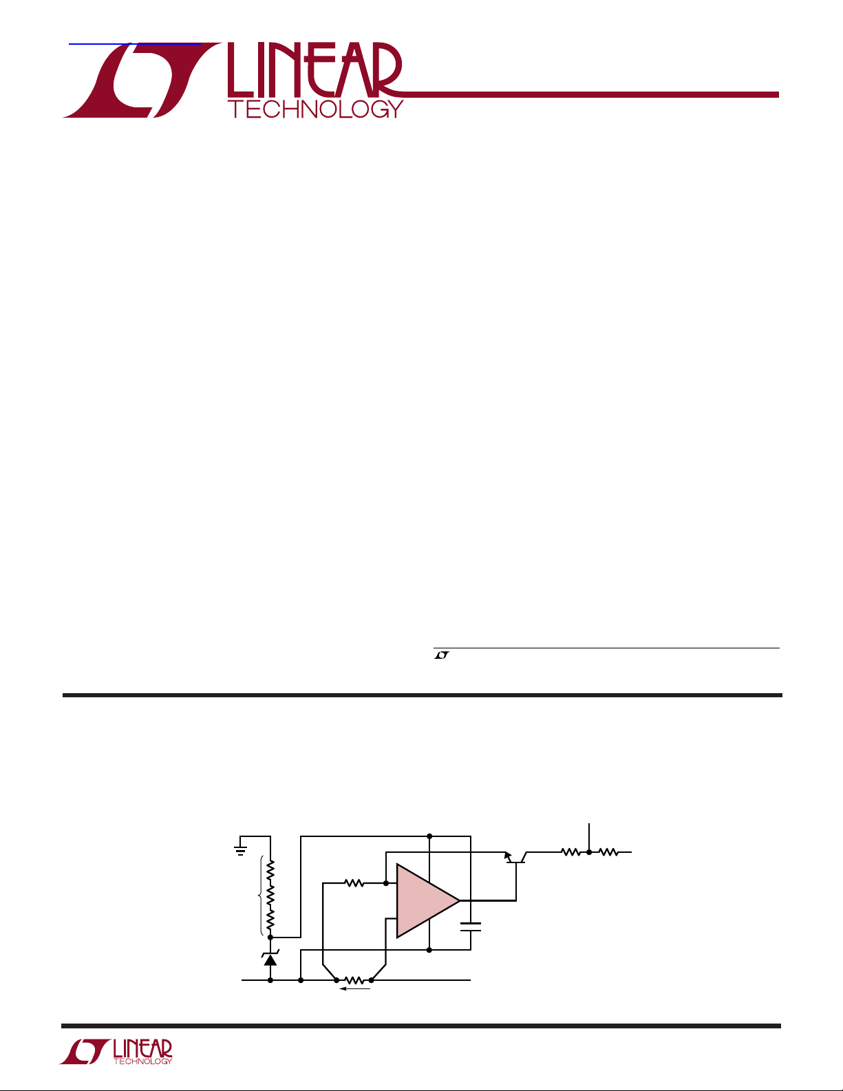
TYPICAL APPLICATION
3.3k
0805
×3
BZX84C6V8
V
= 6.8V
Z
–48V SUPPLY
(–42V TO –56V)
U
Fast Compact –48V Current Sense
FMMT493
30.1Ω
1%
0.003Ω
1% 3W
I
SENSE
–
LT1797
+
0.1µF
–48V LOAD
+–
1797 TA01
= 3V – 0.1Ω • I
V
OUT
I
= 0A TO 30A
SENSE
ACCURACY ≈ 3%
V
OUT
Q1
R1
4.7k
R1 REDUCES Q1 DISSIPATION
SETTLES TO 1% IN 2µs,
1V OUTPUT STEP
1%
SENSE
1k
V
= 3V
S
1
LT1797
WWWU
ABSOLUTE AXI U RATI GS
PACKAGE/ORDER I FOR ATIO
UU
W
(Note 1)
Total Supply Voltage (V+ to V–) ........................... 12.6V
Input Differential Voltage ..................................... 12.6V
Input Current ..................................................... ±10mA
Output Short-Circuit Duration (Note 2)........ Continuous
Operating Temperature Range
(Note 3)
Specified Temperature Range.................
............................................. – 40°C to 85°C
–40°C to 85°C
Junction Temperature........................................... 150°C
TOP VIEW
1
OUT
–
2
+IN
V
T
JMAX
+
3
S5 PACKAGE
5-LEAD PLASTIC SOT-23
= 150°C, θJA = 250°C/W
+
5
V
–
–IN
4
ORDER PART
NUMBER
LT1797CS5
LT1797IS5
S5 PART MARKING
LTLM
LTTL
Storage Temperature Range ................ –65°C to 150°C
Lead Temperature (Soldering, 10 sec)................. 300°C
Consult factory for parts specified with wider operating temperature ranges.
ELECTRICAL CHARACTERISTICS
The ● denotes specifications which apply over the specified temperature range, otherwise specifications are TA = 25°C.
VS = 3V, 0V; VS = 5V, 0V, VCM = V
SYMBOL PARAMETER CONDITIONS MIN TYP MAX UNITS
V
OS
I
B
I
OS
e
n
i
n
R
IN
C
IN
CMRR Common Mode Rejection Ratio VCM = 0V to VS – 1.2V ● 88 96 dB
A
VOL
Input Offset Voltage 1 1.5 mV
Input Offset Voltage Drift (Note 4) ● 520µV/°C
Input Bias Current VCM = V
Input Bias Current Drift ● 0.1 nA/°C
Input Offset Current VCM = V
Input Noise Voltage 0.1Hz to 10Hz 1.5 µV
Input Noise Voltage Density f = 10kHz 20 nV/√Hz
Input Noise Current Density f = 10kHz 0.23 pA/√Hz
Input Resistance Differential 200 330 kΩ
Input Capacitance 4pF
Input Voltage Range ● 0V
Large-Signal Voltage Gain VS = 3V, VO = 0.5V to 2.5V, RL = 10k 200 1000 V/mV
= half supply, pulse power tested, unless otherwise specified. (Note 3)
OUT
≤ 70°C ● 2.5 mV
0°C ≤ T
A
–40°C ≤ T
V
CM
V
CM
f = 10kHz, V
Common Mode, V
V
CM
VS = 5V, VO = 0.5V to 4.5V, RL = 10k 400 1000 V/mV
≤ 85°C ● 3.0 mV
A
–
+
= V
–
+
= V
CM
= 0V to V
= VCC – 0.3V 0.15 pA/√Hz
= 0V to VS – 1.2V 100 MΩ
CM
S
● –300 –150 nA
● 50 100 nA
● 10 25 nA
● 10 25 nA
● 64 72 dB
● 150 V/mV
● 300 V/mV
P-P
S
V
2

LT1797
ELECTRICAL CHARACTERISTICS
The ● denotes specifications which apply over the specified temperature range, otherwise specifications are TA = 25°C.
VS = 3V, 0V; VS = 5V, 0V, VCM = V
SYMBOL PARAMETER CONDITIONS MIN TYP MAX UNITS
PSRR Power Supply Rejection Ratio VS = 2.7V to 12V, VCM = VO= 1V ● 80 90 dB
Minimum Supply Voltage ● 2.5 2.7 V
V
OL
V
OH
I
SC
I
S
GBW Gain Bandwidth Product (Note 5) f = 100kHz 6.0 10 MHz
SR Slew Rate (Note 5) AV = –1 1.3 2.25 V/µs
t
r
t
f
t
S
THD Distortion VS = 3V, V
FPBW Full-Power Bandwidth (Note 6) V
Output Voltage Swing LOW No Load, Input Overdrive = 30mV ● 815 mV
Output Voltage Swing HIGH No Load, Input Overdrive = 30mV ● VS – 0.14 VS – 0.05 V
Short-Circuit Current VS = 5V 25 45 mA
Supply Current 1.1 1.5 mA
Output Rise Time 10% to 90%, 0.1V Step, RL = 10k 55 ns
Output Fall Time 10% to 90%, 0.1V Step, RL = 10k 55 ns
Settling Time VS = 5V, ∆V
= half supply, pulse power tested, unless otherwise specified. (Note 3)
OUT
I
= 5mA ● 80 160 mV
SINK
= 10mA ● 150 250 mV
I
SINK
= 5mA ● VS – 0.30 VS – 0.2 V
I
SOURCE
= 10mA ● VS – 0.39 VS – 0.3 V
I
SOURCE
V
= 3V 15 25 mA
S
● 2.0 mA
≤ 70°C ● 5.0 MHz
0°C ≤ T
A
–40°C ≤ T
0°C ≤ T
–40°C ≤ T
OUT
≤ 85°C ● 4.5 MHz
A
≤ 70°C ● 1.1 V/µs
A
≤ 85°C ● 1.0 V/µs
A
= 2V to 0.1%, AV = –1 1.6 µs
OUT
= 2V
OUT
P-P
= 1.8V
, AV = 1, RL = 10k, f = 1kHz 0.001 %
P-P
360 kHz
The ● denotes specifications which apply over the specified temperature range, otherwise specifications are TA = 25°C.
VS = ±5V, VCM = 0V, V
SYMBOL PARAMETER CONDITIONS MIN TYP MAX UNITS
V
OS
I
B
I
OS
e
n
i
n
R
IN
C
IN
Input Offset Voltage 1 1.5 mV
Input Offset Voltage Drift (Note 4) ● 520µV/°C
Input Bias Current VCM = V
Input Bias Current Drift ● 0.1 nA/°C
Input Offset Current VCM = V
Input Noise Voltage 0.1Hz to 10Hz 1 µV
Input Noise Voltage Density f = 10kHz 20 nV/√Hz
Input Noise Current Density f = 10kHz 0.23 pA/√Hz
Input Resistance Differential 200 330 kΩ
Input Capacitance 4pF
Input Voltage Range ● –5 5 V
= 0V, pulse power tested unless otherwise specified. (Note 3)
OUT
≤ 70°C ● 2.5 mV
0°C ≤ T
A
–40°C ≤ T
V
CM
V
CM
f = 10kHz, V
Common Mode, V
≤ 85°C ● 3.0 mV
A
–
+
= V
–
+
= V
= 4.7V 0.15 pA/√Hz
CM
= –5V to 3.8V 100 MΩ
CM
● –300 –150 nA
● 50 100 nA
● 10 25 nA
● 10 25 nA
P-P
3
LT1797
ELECTRICAL CHARACTERISTICS
The ● denotes specifications which apply over the specified temperature range, otherwise specifications are TA = 25°C.
VS = ±5V, VCM = 0V,V
SYMBOL PARAMETER CONDITIONS MIN TYP MAX UNITS
CMRR Common Mode Rejection Ratio VCM = –5V to 3.8V ● 83 96 dB
A
VOL
V
OL
V
OH
I
SC
PSRR Power Supply Rejection Ratio VS = ±1.35V to ±6V ● 80 90 dB
I
S
GBW Gain Bandwidth Product f = 100kHz 6.5 11 MHz
SR Slew Rate AV = –1, RL = ∞, VO = ±4V, Measured at VO = ±2V 1.50 2.50 V/µs
t
r
t
f
t
S
FPBW Full-Power Bandwidth (Note 6) V
Note 1: Absolute Maximum Ratings are those values beyond which the life
of a device may be impaired.
Note 2: A heat sink may be required to keep the junction temperature
below absolute maximum.
Note 3: The LT1797C is guaranteed to meet 0°C to 70°C specifications
and is designed, characterized and expected to meet the extended
temperature limits, but is not tested at –40°C and 85°C. The LT1797I is
guaranteed to meet specified performance from –40°C to 85°C.
Large-Signal Voltage Gain VO = ±4V, RL = 10k 400 1000 V/mV
Output Voltage Swing LOW No Load, Input Overdrive = 30mV ● –4.99 – 4.98 V
Output Voltage Swing HIGH No Load, Input Overdrive = 30mV ● 4.84 4.95 V
Short-Circuit Current (Note 2) Short to GND 30 50 mA
Supply Current 1.40 2.25 mA
Output Rise Time 10% to 90%, 0.1V Step, RL = 10k 55 ns
Output Fall Time 10% to 90%, 0.1V Step, RL = 10k 55 ns
Settling Time ∆V
= 0V, pulse power tested unless otherwise specified. (Note 3)
OUT
= –5V to 5V ● 66 76 dB
V
CM
I
= 5mA ● –4.92 –4.87 V
SINK
= 10mA ● –4.85 –4.79 V
I
SINK
= 5mA ● 4.70 4.80 V
I
SOURCE
I
= 10mA ● 4.61 4.70 V
SOURCE
0°C ≤ T
≤ 70°C ● 5.5 MHz
A
–40°C ≤ T
0°C ≤ T
–40°C ≤ T
OUT
≤ 85°C ● 5.0 MHz
A
≤ 70°C ● 1.25 V/µs
A
≤ 85°C ● 1.10 V/µs
A
= 4V to 0.1%, AV = 1 2.6 µs
OUT
= 8V
P-P
Note 4: This parameter is not 100% tested.
Note 5: V
= 3V limit guaranteed by correlation to 5V tests.
S
Note 6: Full-power bandwidth is calculated from the slew rate:
FPBW = SR/2πV
● 300 V/mV
● 2.70 mA
100 kHz
P
4

UW
COMMON MODE VOLTAGE (V)
–200
INPUT BIAS CURRENT (nA)
–100
0
100
–150
–50
50
1.0 2.0 3.0 4.0
1797 G03
5.00.50 1.5 2.5 3.5 4.5
VS = 5V, 0V
TA = 25°C
T
A
= 125°C
TA = –55°C
TYPICAL PERFOR A CE CHARACTERISTICS
Supply Current vs Supply Voltage Minimum Supply Voltage
–100
–200
INPUT OFFSET VOLTAGE CHANGE (µV)
–300
300
200
100
0
TA = 125°C
TA = 25°C
1.0 1.5 2.0 3.0 4.0
TOTAL SUPPLY VOLTAGE (V)
TA = –55°C
1.8
1.6
1.4
1.2
1.0
0.8
0.6
SUPPLY CURRENT (mA)
0.4
0.2
0
12345 101112
0
TA = 125°C
6789
TOTAL SUPPLY VOLTAGE (V)
TA = 25°C
TA = –55°C
1797 G01
LT1797
Input Bias Current
vs Common Mode Voltage
5.00.50 2.5 3.5 4.5
1797 G02
Output Saturation Voltage
vs Load Current (Output High)
1
VS = ±2.5V
V
OD
0.1
TA = 125°C
TA = –55°C
OUTPUT SATURATION VOLTAGE (V)
0.01
1µ
Output Short-Circuit Current
vs Temperature 0.1Hz to 10Hz Noise Voltage
50
VS = ±2.5V
45
40
35
30
OUTPUT CURRENT (mA)
25
20
–50
= 30mV
TA = 25°C
SOURCING LOAD CURRENT (A)
–25 0
100µ10µ 10m1m
SOURCING CURRENT
SINKING CURRENT
TEMPERATURE (°C)
50 100 125
25 75
1797 G04
1797 G07
Output Saturation Voltage
vs Load Current (Output Low)
1
VS = ±2.5V
V
= 30mV
OD
0.1
TA = 125°C
0.01
TA = 25°C
OUTPUT SATURATION VOLTAGE (V)
0.001
1µ 100µ 1m 10m
10µ
SINKING LOAD CURRENT (A)
VS = ±5V
NOISE VOLTAGE (1µV/DIV)
2468
TIME (SEC)
TA = –55°C
1797 G05
1797 G08
10103579
Output Saturation Voltage
vs Input Overdrive
150
140
130
120
110
100
90
80
70
60
50
40
30
20
OUTPUT SATURATION VOLTAGE (mV)
10
0
0
30 50 100
10 20
INPUT OVERDRIVE (mV)
40
OUTPUT HIGH
OUTPUT LOW
60 70 80 90
Input Noise Voltage Density
vs Frequency
100
VS = ±2.5V
80
60
40
20
INPUT NOISE VOLTAGE DENSITY (nV/√Hz)
0
10 1k 10k 100k
100
FREQUENCY (Hz)
VS = ±2.5V
I
= 0
OUT
1797 G06
1797 G09
5

LT1797
TEMPERATURE (°C)
–50
GAIN BANDWIDTH PRODUCT (MHz)
11.5
25
1797 G12
10.0
9.0
–25 0 50
8.5
8.0
12.0
11.0
10.5
9.5
75 100 125
VS = ±5V
VS = ±2.5V
f = 100kHz
UW
TYPICAL PERFOR A CE CHARACTERISTICS
Input Noise Current Density
vs Frequency
1.2
1.0
0.8
0.6
0.4
0.2
INPUT NOISE CURRENT DENSITY (pA/√Hz)
0
10 1k 10k 100k
100
FREQUENCY (Hz)
Slew Rate vs Temperature
3.5
VS = ±2.5V
3.0
2.5
2.0
SLEW RATE (V/µs)
1.5
1.0
–50 –25
RISING
FALLING
50
25
0
TEMPERATURE (°C)
75
VS = ±2.5V
1797 G10
100
1797 G13
Gain and Phase Shift
vs Frequency
70
60
50
40
30
20
GAIN (dB)
10
0
–10
–20
–30
10k 1M 10M 100M
100k
Gain Bandwidth Product and
Phase Margin vs Supply Voltage
f = 100kHz
= RG = 1k
R
F
13
12
11
10
GAIN BANDWIDTH PRODUCT (MHz)
125
GAIN BANDWIDTH PRODUCT
9
8
0
3
2
TOTAL SUPPLY VOLTAGE (V)
GAIN
FREQUENCY (Hz)
PHASE MARGIN
5 7 9 11 12
468
VS = ±2.5V
PHASE
101
1797 G11
1797 G14
100
80
60
40
PHASE (DEG)
20
0
–20
–40
–60
–80
–100
60
55
50
PHASE MARGIN (DEG)
45
40
35
30
14
13
12
GAIN BANDWIDTH PRODUCT (MHz)
11
10
1k
Gain Bandwidth Product
vs Temperature
Gain Bandwidth Product and
Phase Margin vs RF and R
VS = ±5V
PHASE MARGIN
GAIN BANDWIDTH PRODUCT
10k 100k
RF = RG = (Ω)
G
1797 G15
60
50
40
PHASE MARGIN (DEG)
30
20
10
PSRR vs Frequency CMRR vs Frequency
90
80
70
60
50
POSITIVE SUPPLY
40
30
20
10
0
POWER SUPPLY REJECTION RATIO (dB)
–10
1k 100k 1M 10M
6
10k
NEGATIVE SUPPLY
FREQUENCY (Hz)
VS = ±2.5V
1797 G16
110
100
90
80
70
60
50
40
30
20
COMMON MODE REJECTION RATIO (dB)
10
1k 100k 1M 10M
10k
FREQUENCY (Hz)
VS = ±2.5V
1797 G17
Output Impedance vs Frequency
100
VS = ±2.5V
10
1
0.1
OUTPUT IMPEDANCE (Ω)
0.01
100 1k
GAIN = 100
GAIN = 10
10k 100k 1M 10M
FREQUENCY (Hz)
1797 G18

UW
LOAD RESISTANCE TO GROUND (kΩ)
0.01
THD + NOISE (%)
0.1
1
10
1 10 100
1797 G24
0.001
0.1
VS = 3V, 0V
V
IN
= 1.8V
P-P
VCM = 1.5V
VS = 3V, 0V
V
IN
= 1.8V
P-P
VCM = 1V
V
S
= 3V TOTAL
A
V
= 1
f = 1kHz
TYPICAL PERFOR A CE CHARACTERISTICS
LT1797
Open-Loop Gain
RL = 50k
RL = 10k
RL = 2k
CHANGE IN INPUT OFFSET VOLTAGE (50µV/DIV)
–5
–4 –3 –2 –1
012
OUTPUT VOLTAGE (V)
345
Undistorted Output Swing
vs Frequency
12
AV = 1
11
10
9
)
P-P
8
7
6
5
4
OUTPUT SWING (V
3
2
1
0
100 10k 100k 1M
VS = ±5V
VS = ±1.5V
1k
FREQUENCY (Hz)
VS = ±5V
1797 G19
1797 G22
Settling Time
to 0.1% vs Output Step
4
VS = ±5V
3
AV = 1
2
1
0
–1
OUTPUT STEP (V)
–2
–3
– 4
AV = 1
1.4 1.8 2.2 3.02.41.2 1.6 2.0 2.8
1.0
SETTLING TIME (µs)
= –1
A
V
AV = –1
Total Harmonic Distortion + Noise
vs Frequency
1
RL = 10k
= 3V, 0V
V
S
= 1.8V
V
OUT
VCM = 1V
0.1
0.01
THD + NOISE (%)
0.001
0.0001
10 100
P-P
AV = –1
AV = 1
1k 10k 100k
FREQUENCY (Hz)
2.6
1797 G20
1797 G23
Capacitive Load Handling
Overshoot vs Capacitive Load
50
VS = ±2.5V
45
40
35
30
25
20
OVERSHOOT (%)
15
10
5
0
10
AV = 1
AV = 5
AV = 10
100 1000 10000
CAPACITIVE LOAD (pF)
AV = 2
Total Harmonic Distortion + Noise
vs Load Resistance
1797 G21
Total Harmonic Distortion + Noise
vs Output Voltage Amplitude
10
1
AV = –1
= 3V, 0V
V
S
0.1
THD + NOISE (%)
0.01
0.001
023
OUTPUT VOLTAGE (V
AV = 1
= 3V, 0V
V
S
1
AV = 1
= ±1.5V
V
S
f = 1kHz
= HALF SUPPLY
V
CM
= 10k
R
L
V
P-P
AV = –1
= ±1.5V
S
)
1797 G25
Large-Signal Response
VS = ±2.5V
A
= 1
V
1797 G26
Small-Signal Response
V
= ±2.5V
S
= 1
A
V
R
= 10k
L
1797 G27
7

LT1797
WUUU
APPLICATIO S I FOR ATIO
Supply Voltage
The positive supply pin of the LT1797 should be bypassed
with a small capacitor (about 0.1µF) within an inch of the
pin. When driving heavy loads an additional 4.7µF electro-
lytic capacitor should be used. When using split supplies
the same is true for the negative supply pin.
Inputs
The LT1797 is fully functional for an input signal range
from the negative supply to the positive supply. Figure 1
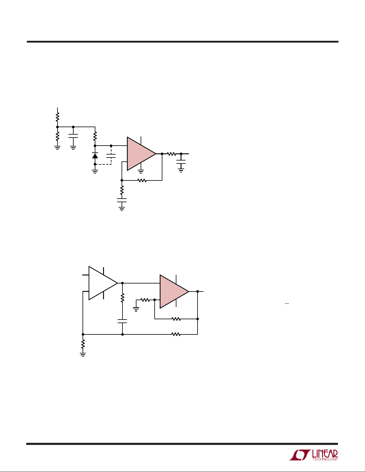
shows a simplified schematic of the amplifier. The input
stage consists of two differential amplifiers, a PNP stage
Q3/Q4 and an NPN stage Q1/Q2 that are active over
different ranges of input common mode voltage. The PNP
differential pair is active for input common mode voltages
VCM between the negative supply to approximately 1.2V
below the positive supply. As VCM moves closer toward
the positive supply, the transistor QB1 will steer the tail
current I1 to the current mirror Q5/Q6, activating the NPN
differential pair and the PNP pair becomes inactive for the
rest of the input common mode range up to the positive
supply.
The input offset voltage and the input bias current are
dependent on which input stage is active. The input offset
voltage is trimmed on a single 5V supply with the common
mode at 1/2 supply and is typically 1mV with the PNP stage
active. The input offset of the NPN stage is untrimmed and
is typically 1.5mV. The input bias current polarity depends
on the input common mode voltage. When the PNP
differential pair is active, the input bias currents flow out
of the input pins. They flow in the opposite direction when
the NPN input stage is active. The offset error due to the
input bias currents can be minimized by equalizing the
noninverting and inverting source impedance.
The input stage of the LT1797 incorporates phase reversal
protection to prevent false outputs from occurring when
the inputs are driven up to 5V beyond the rails. Protective
resistors are included in the input leads so that current
does not become excessive when the inputs are forced
beyond the supplies or when a large differential signal is
applied.
Output
The output is configured with a pair of complementary
common emitter stages Q19/Q20, which enable the output to swing from rail-to-rail. The output voltage swing of
the LT1797 is affected by input overdrive as shown in the
Typical Performance Characteristics. When monitoring
input voltages within 50mV of V+ or within 8mV of V–,
some gain should be taken to keep the output from
clipping. The output of the LT1797 can deliver large load
currents; the short-circuit current limit is typically 50mA at
±5V. Take care to keep the junction temperature of the IC
below the absolute maximum rating of 150°C. The output
of the amplifier has reverse biased diodes to each supply.
If the output is forced beyond either supply, unlimited
current will flow through these diodes.
The LT1797 can drive capacitive loads up to 200pF on a
single 5V supply in a unity gain configuration. When there
is a need to drive larger capacitive loads, a resistor of a
couple hundred ohms should be connected between the
output and the capacitive load. The feedback should still be
taken from the output so that the resistor isolates the
capacitive load to ensure stability. The low input bias
current of the LT1797 makes it possible to use high value
feedback resistors to set the gain. However, care must be
taken to insure that the pole formed by the feedback
resistors and the total capacitance at the inverting input
does not degrade stability.
8

WUUU
APPLICATIO S I FOR ATIO
LT1797
Distortion
There are two main contributors to distortion in op amps:
output crossover distortion as the output transitions from
sourcing to sinking current and distortion caused by
nonlinear common mode rejection. If the op amp is
operating in the inverting mode, there is no common mode
induced distortion. If the op amp is operating in the PNP
input stage (input is not within 1.2V of V+), the CMRR is
I1
BIAS
–IN
+IN
R1
QB1
R5
D1
R6
D2
Q1
R2
Q13
Q2
Q3 Q4
very good, typically 95dB. When the LT1797 switches
between input stages there is significant nonlinearity in the
CMRR. Lower load resistance increases the output crossover distortion, but has no effect on the input stage
transition distortion. For lowest distortion the LT1797
should be operated single supply, with the output always
sourcing current and with the input voltage swing between
ground and (V+ – 1.2V). See the Typical Performance
Characteristic curves.
Q9
1/2 SUPPLY
Q14
Q10
Q18
Q15
I3I2
+1 +1
Q17
Q16
I7
R7 R8
Q19
C2
CM
OUT
I4 I5
Q8
Q7
Q11
Q5
Q6
R3 R4
Q12
C1
Q20
I6
1797 F01
Figure 1. Simplified Schematic
9
LT1797
TYPICAL APPLICATIO S
3V
R2
1k
R3
10k
C1
0.1µF
PHOTODIODE
SFH213FA
R1
100k
C
*
P
U
Single Supply Hi-Gain 80kHz Photodiode Amplifier
*CP = SUM OF PHOTODIODE CAPACITANCE, PARASITIC LAYOUT
CAPACITANCE AND LT1797 INPUT CAPACITANCE ≅10pF.
TRANSIMPEDANCE GAIN: A
R6, C3 LIMIT THE NOISE BANDWIDTH TO 500kHz.
C3
1000pF
1797 TA02
OUTPUT NOISE ≅1.8mV
R1, C
AND LT1797 GBW SET UPPER LIMIT ON BANDWIDTH.
P
R4, C2 SET LOWER 1.6kHz LIMIT ON GAIN OF 101.
R4
1k
+
LT1797
–
C2
0.1µF
3V
R5
100k
R6
330Ω
RMS
= 10MΩ.
Z
.
Ultra-Low Noise, ±5V Supply, Rail-to-Rail Output Amplifier
5V
+
–
5V
LT1797
–5V
R1
10k
R3
4.99k
OUT
TOTAL INPUT VOLTAGE NOISE ≅ 0.94nV/√Hz
(INCLUDING 10Ω RESISTOR)
BANDWIDTH ≅ 40kHz
= 500
A
V
1797 TA03
+
IN
LT1028
–
–5V
R4
10Ω
R5
1k
C1
2200pF
R2
4.99k
10

PACKAGE DESCRIPTIO
LT1797
U
Dimensions in inches (millimeters) unless otherwise noted.
S5 Package
5-Lead Plastic SOT-23
(LTC DWG # 05-08-1633)
2.80 – 3.00
(0.110 – 0.118)
(NOTE 3)
1.90
2.60 – 3.00
(0.102 – 0.118)
1.50 – 1.75
(0.059 – 0.069)
0.35 – 0.55
(0.014 – 0.022)
NOTE:
1. DIMENSIONS ARE IN MILLIMETERS
2. DIMENSIONS ARE INCLUSIVE OF PLATING
3. DIMENSIONS ARE EXCLUSIVE OF MOLD FLASH AND METAL BURR
4. MOLD FLASH SHALL NOT EXCEED 0.254mm
5. PACKAGE EIAJ REFERENCE IS SC-74A (EIAJ)
0.09 – 0.20
(0.004 – 0.008)
(NOTE 2)
(0.074)
REF
0.00 – 0.15
(0.00 – 0.006)
0.35 – 0.50
(0.014 – 0.020)
FIVE PLACES (NOTE 2)
0.95
(0.037)
REF
0.90 – 1.45
(0.035 – 0.057)
0.90 – 1.30
(0.035 – 0.051)
S5 SOT-23 0599
Information furnished by Linear Technology Corporation is believed to be accurate and reliable.
However, no responsibility is assumed for its use. Linear Technology Corporation makes no representation that the interconnection of its circuits as described herein will not infringe on existing patent rights.
11

LT1797
TYPICAL APPLICATIO
1MHz Photodiode Transimpedance Amplifier
U
Response of Photodiode Amplifier
PHOTODIODE
SFH213FA
SIEMENS/INFINEON
–
+
3pF
100k
V
LT1797
V
+
–
= ±1.5V TO ±5V
V
S
1797 TA04
100mV/DIV
2µs/DIV
Rise Time vs Supply Voltage (600mV Output Step)
Supply Voltage 10% to 90% Rise Time
±1.5V 830ns
±2.5V 800ns
±5V 700ns
RELATED PARTS
PART NUMBER DESCRIPTION COMMENTS
LT1630/LT1631 Dual/Quad 30MHz, 10V/µs Rail-to-Rail Input High DC Accuracy, 525µV V
and Output Op Amps Current, Max Supply Current 4.4mA per Amp
LT1638/LT1639 Dual/Ouad 1.2MHz, 0.4V/µs, Over-The-TopTM Micropower 170µA Supply Current, Single Supply Input Range –0.4V to 44V,
Rail-to-Rail Input and Output Op Amps Rail-to-Rail Input and Output.
LT1783 Micropower Over-The-Top SOT-23 Rail-to-Rail Input SOT-23 Package, Micropower 220µA per Amplifier,
and Output Op Amp Rail-to-Rail Input and Output, 1.2MHz Gain Bandwidth
LT1880 SOT-23 Rail-to-Rail Output, Picoamp Input Current 150mV Maximum Offset Voltage, 900pA Maximum Bias Current,
Precision Op Amp 1.1MHz Gain Bandwidth, –40°C to 85°C Temperature Range
Over-The-Top is a trademark of Linear Technology Corporation.
OS(MAX)
, 70mA Output
12
Linear Technology Corporation
1630 McCarthy Blvd., Milpitas, CA 95035-7417
(408) 432-1900 ● FAX: (408) 434-0507
●
www.linear-tech.com
1797f LT/TP 0401 4K • PRINTED IN USA
LINEAR TECHNOLOGY CORPORATION 2000
 Loading...