

Linear Technology LT1795 Datasheet
FEATURES
LT1795
Dual 500mA/50MHz
Current Feedback Line Driver
Amplifier
U
DESCRIPTIO
■
500mA Output Drive Current
■
50MHz Bandwidth, AV = 2, RL = 25
■
900V/µs Slew Rate, AV = 2, RL = 25
■
Low Distortion: –75dBc at 1MHz
■
High Input Impedance, 10MΩ
■
Wide Supply Range, ±5V to ±15V
■
Full Rate, Downstream ADSL Supported
■
Power Enhanced Small Footprint Packages
Ω
Ω
TSSOP-20, S0-20 Wide
■
Low Power Shutdown Mode
■
Power Saving Adjustable Supply Current
■
Stable with CL = 10,000pF
U
APPLICATIO S
■
ADSL HDSL2, G.lite Drivers
■
Buffers
■
Test Equipment Amplifiers
■
Video Amplifiers
■
Cable Drivers
U
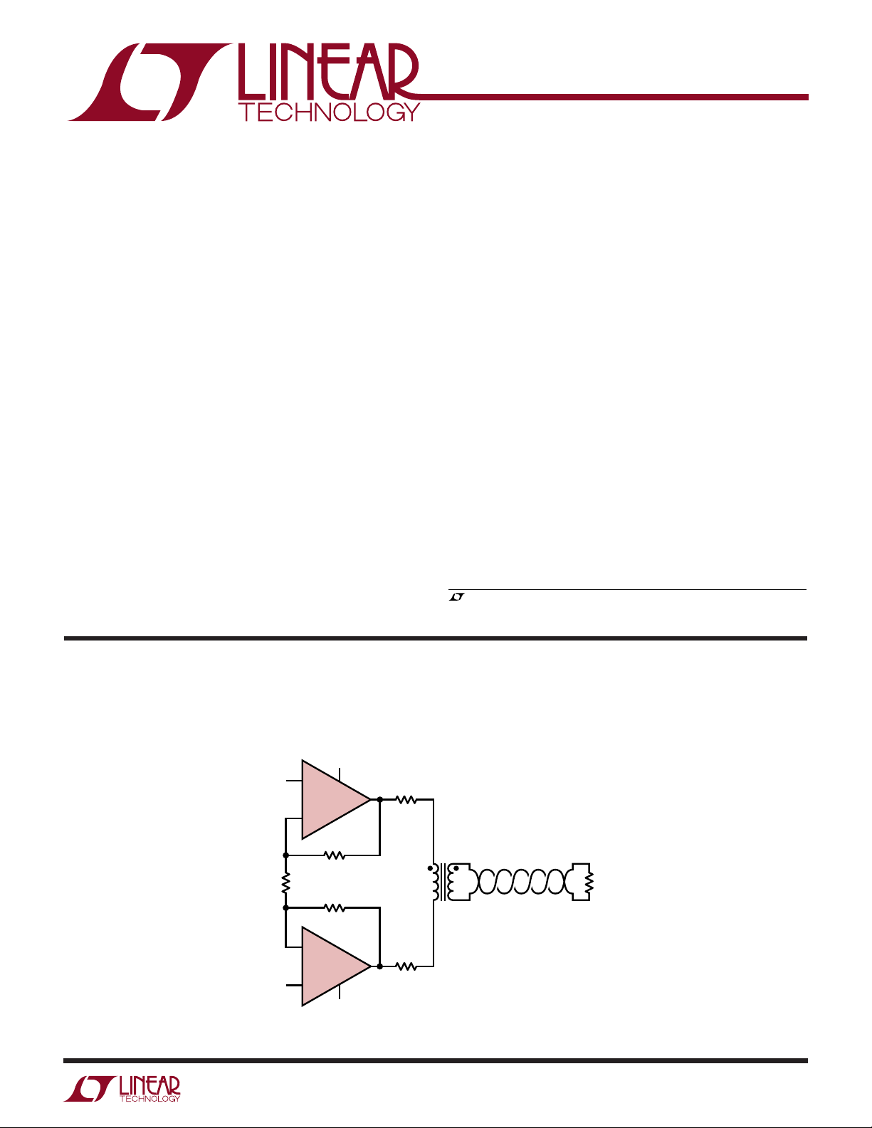
TYPICAL APPLICATION
The LT®1795 is a dual current feedback amplifier with high
output current and excellent large signal characteristics.
The combination of high slew rate, 500mA output drive
and up to ±15V operation enables the device to deliver
significant power at frequencies in the 1MHz to 2MHz
range. Short-circuit protection and thermal shutdown
insure the device’s ruggedness. The LT1795 is stable with
large capacitive loads and can easily supply the large
currents required by the capacitive loading. A shutdown
feature switches the device into a high impedance, low
current mode, reducing power dissipation when the device is not in use. For lower bandwidth applications, the
supply current can be reduced with a single external
resistor.
The LT1795 comes in the very small, thermally enhanced,
20-lead TSSOP package for maximum port density in line
driver applications.
, LTC and LT are registered trademarks of Linear Technology Corporation.
Low Loss, High Power Central Office ADSL Line Driver
+
V
+IN
+
1/2
LT1795
–
1k
165Ω
1k
–
1/2
–IN
* MIDCOM 50215 OR EQUIVALENT
LT1795
+
–
V
12.5Ω
1:2*
12.5Ω
100Ω
1795 TA01
1

LT1795
WW
W
ABSOLUTE AXI U RATI GS
U
(Note 1)
Supply Voltage ...................................................... ±18V
Input Current ...................................................... ±15mA
Output Short-Circuit Duration (Note 2)............ Indefinite
Operating Temperature Range ................ –40°C to 85°C
UUW
PACKAGE/ORDER I FOR ATIO
–IN
+IN
SHDN
SHDNREF
+IN
–IN
TOP VIEW
–
1
V
2
NC
3
4
5
6
7
8
9
NC
–
10
V
FE PACKAGE
20-LEAD PLASTIC TSSOP
T
= 150° C, θJA = 40°C/W (Note 4)
JMAX
–
20
V
19
NC
18
OUT
+
17
V
16
COMP
15
COMP
+
14
V
13
OUT
12
NC
–
11
V
ORDER PART
NUMBER
LT1795CFE
LT1795IFE
Specified Temperature Range (Note 3)... – 40°C to 85°C
Junction Temperature........................................... 150°C
Storage Temperature Range ................. –65°C to 150°C
Lead Temperature (Soldering, 10 sec).................. 300°C
TOP VIEW
1
COMP
+
2
V
3
OUT
–
4
V
–
5
V
–
6
V
–
7
V
8
–IN
9
+IN
10
SHDN
S PACKAGE
20-LEAD PLASTIC SW
T
= 150° C, θJA ≈ 40°C/W (Note 4)
JMAX
20
19
18
17
16
15
14
13
12
11
COMP
+
V
OUT
–
V
–
V
–
V
–
V
–IN
+IN
SHDNREF
ORDER PART
NUMBER
LT1795CSW
LT1795ISW
Consult factory for Military grade parts.
ELECTRICAL CHARACTERISTICS
The ● denotes the specifications which apply over the full specified temperature range, otherwise specifications are at TA = 25°C.
VCM = 0V, ±5V ≤ VS ≤ ±15V, pulse tested, V
SYMBOL PARAMETER CONDITIONS MIN TYP MAX UNITS
V
I
I
e
+i
–i
OS
+
IN
–
IN
n
n
n
Input Offset Voltage ±3 ±13 mV
Input Offset Voltage Matching ±1 ±3.5 mV
Input Offset Voltage Drift ● 10 µV/°C
Noninverting Input Current ±2 ±5 µA
Noninverting Input Current Matching ±0.5 ±2 µA
Inverting Input Current ±10 ±70 µA
Inverting Input Current Matching ±10 ±30 µA
Input Noise Voltage Density f = 10kHz, RF =1k, RG = 10Ω, RS = 0Ω 3.6 nV/√Hz
Input Noise Current Density f = 10kHz, RF =1k, RG = 10Ω, RS = 10kΩ 2 pA/√Hz
Input Noise Current Density f = 10kHz, RF =1k, RG = 10Ω, RS = 10kΩ 30 pA/√Hz
SHDN
= 2.5V, V
SHDNREF
= 0V unless otherwise noted. (Note 3)
● ±4.5 ±17 mV
● ±1.5 ±5.0 mV
● ±8 ±20 µA
● ±1.5 ±7 µA
● ±20 ±100 µA
● ±20 ±50 µA
2
LT1795
ELECTRICAL CHARACTERISTICS
The ● denotes the specifications which apply over the full specified temperature range, otherwise specifications are at TA = 25°C.
VCM = 0V, ±5V ≤ VS ≤ ±15V, pulse tested, V
SYMBOL PARAMETER CONDITIONS MIN TYP MAX UNITS
+
R
IN
+
C
IN
CMRR Common Mode Rejection Ratio VS = ±15V, VCM = ±12V ● 55 62 dB
PSRR Power Supply Rejection Ratio VS = ±5V to ±15V ● 60 77 dB
A
V
R
OL
V
OUT
I
OUT
I
S
HD2, HD
3
SR Slew Rate (Note 7) AV = 4, RL = 400Ω 400 900 V/µs
BW Small-Signal BW AV = 2, VS = ±15V, Peaking ≤ 1.5dB 65 MHz
Input Resistance VIN = ±12V, VS = ±15V ● 1.5 10 MΩ
Input Capacitance VIN = ±15V 2 pF
Input Voltage Range (Note 5) VS = ±15V ● ±12 ±13.5 V
Inverting Input Current VS = ±15V, VCM = ±12V ● 110µA/V
Common Mode Rejection V
Noninverting Input Current VS = ±5V to ±15V ● 30 500 nA/V
Power Supply Rejection
Inverting Input Current VS = ±5V to ±15V ● 15µA/V
Power Supply Rejection
Large-Signal Voltage Gain VS = ±15V, V
Transresistance, ∆V
OUT
/∆I
–
IN
Maximum Output Voltage Swing VS = ±15V, RL = 25Ω±11.5 ±12.5 V
Maximum Output Current VS = ±15V, RL = 1Ω ● 0.5 1 A
Supply Current Per Amplifier VS = ±15V, V
Supply Current Per Amplifier, VS = ±15V 15 20 mA
= 51k, (Note 6) ● 25 mA
R
SHDN
Positive Supply Current, Shutdown VS = ±15V, V
Output Leakage Current, Shutdown VS = ±15V, V
Channel Separation VS = ±15V, V
2nd and 3rd Harmonic Distortion f = 1MHz, VO = 20V
Differential Mode
Slew Rate AV = 4, RL = 25Ω 900 V/µs
SHDN
= 2.5V, V
SHDNREF
= 0V unless otherwise noted. (Note 3)
V = ±2V, VS = ±5V ● 0.5 5 MΩ
VS = ±5V ● ±2 ±3.5 V
VS = ±5V, VCM = ±2V ● 50 60 dB
= ±5V, VCM = ±2V ● 110µA/V
S
= ±10V, RL = 25Ω ● 55 68 dB
= ±5V, V
V
S
VS = ±15V, V
VS = ±5V, V
OUT
= ±2V, RL = 12Ω ● 55 68 dB
OUT
= ±10V, RL = 25Ω ● 75 200 kΩ
OUT
= ±2V, RL = 12Ω ● 75 200 kΩ
OUT
● ±10.0 ±11.5 V
VS = ±5V, RL = 12Ω±2.5 ±3V
● ±2.0 ±3V
= 2.5V 29 34 mA
SHDN
= 0.4V ● 1 200 µA
SHDN
= 0.4V 1 10 µA
SHDN
= ±10V, RL = 25Ω 80 110 dB
OUT
, RL = 50, AV = 2 –75 dBc
P-P
● 42 mA
RF = RG = 910Ω, RL = 100Ω
AV = 2, VS = ±15V, Peaking ≤ 1.5dB 50 MHz
= RG = 820Ω, RL = 25Ω
R
F
Note 1: Absolute Maximum Ratings are those values beyond which the life
of a device may be impaired.
Note 2: Applies to short-circuits to ground only. A short-circuit between
the output and either supply may permanently damage the part when
operated on supplies greater than ±10V.
Note 3: The LT1795C is guaranteed to meet specified performance from
0°C to 70°C and is designed, characterized and expected to meet these
extended temperature limits, but is not tested at –40°C and 85°C. The
LT1795I is guaranteed to meet the extended temperature limits.
Note 4: Thermal resistance varies depending upon the amount of PC board
metal attached to the device. If the maximum dissipation of the package is
exceeded, the device will go into thermal shutdown and be protected.
Note 5: Guaranteed by the CMRR tests.
Note 6: R
is connected between the SHDN pin and V+.
SHDN
Note 7: Slew rate is measured at ±5V on a ±10V output signal while
operating on ±15V supplies with R
R
= 400Ω.
L
= 1k, RG = 333Ω (AV = +4) and
F
3
LT1795
W
UU
SMALL-SIGNAL BANDWIDTH
RSD = 0Ω, IS = 30mA per Amplifer, VS = ±15V,
Peaking ≤ 1dB, RL = 25Ω
A
V
R
F
–1 976 976 44
1 1.15k — 53
2 976 976 48
10 649 72 46
R
G
–3dB BW
(MHz)
RSD = 51kΩ, IS = 15mA per Amplifer, VS = ±15V,
Peaking ≤ 1dB, RL = 25Ω
A
V
–1 976 976 30
1 1.15k — 32
2 976 976 32
10 649 72 27
UW
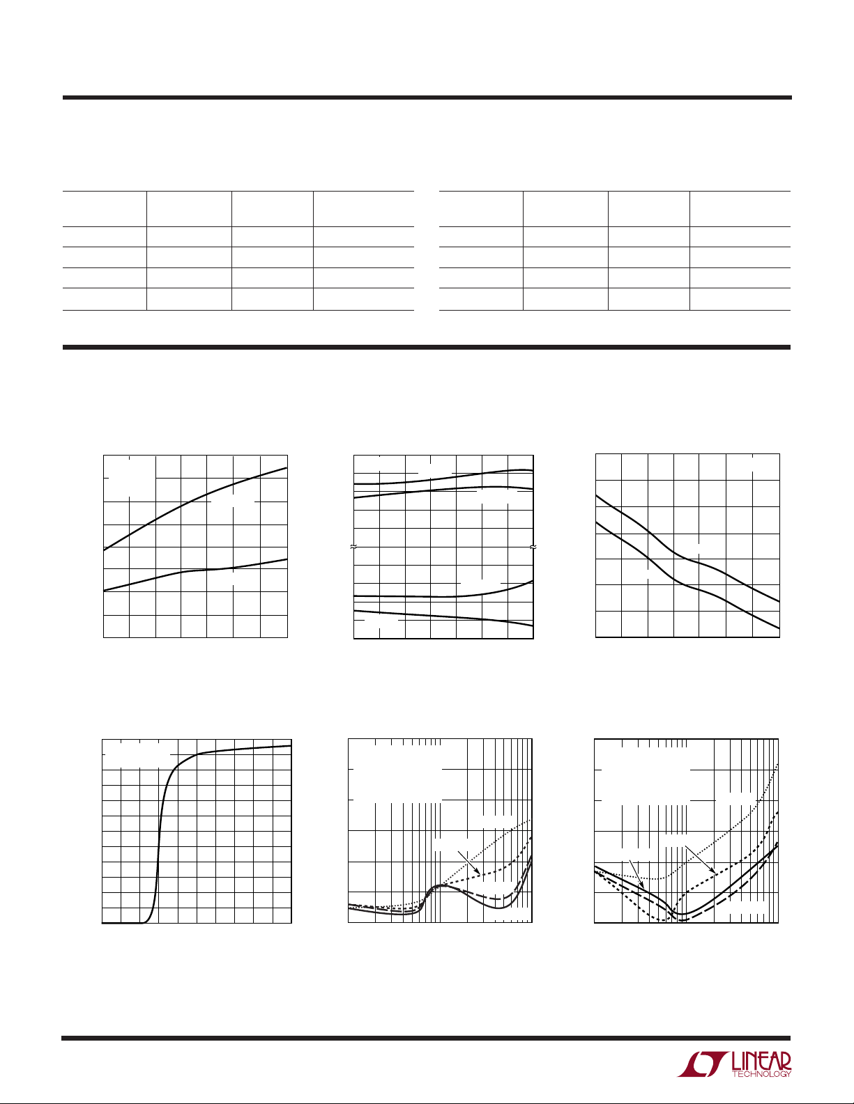
TYPICAL PERFOR A CE CHARACTERISTICS
Supply Current vs Ambient
Temperature
40
VS = ±15V
= 1
A
35
V
= ∞
R
L
30
25
20
15
10
5
SUPPLY CURRENT PER AMPLIFIER (mA)
0
–50
–25 0
TEMPERATURE (°C)
RSD = 0Ω
RSD = 51kΩ
50 100 125
25 75
LT1795 G01
Output Saturation Voltage vs
Junction Temperature
+
V
VS = ±15V
–1
–2
–3
–4
4
3
2
OUTPUT SATURATION VOLTAGE (V)
1
RL = 2k
–
V
–50
–25
RL = 2k
50
25
0
TEMPERATURE (°C)
RL = 25Ω
RL = 25Ω
75
100
LT1795 G02
125
R
F
R
G
Output Short-Circuit Current vs
Junction Temperature
2.0
1.8
1.6
1.4
1.2
–50
SINKING
–25 0
1.0
0.8
OUTPUT SHORT-CIRCUIT CURRENT (A)
0.6
SOURCING
25 75
TEMPERATURE (°C)
–3dB BW
(MHz)
VS = ±15V
50 100 125
LT1795 G03
SHDN Pin Current vs Voltage
0.6
VS = ±15V
= 0V
V
SHDNREF
0.5
0.4
0.3
0.2
CURRENT INTO SHDN PIN (mA)
0.1
0
0
1 2 3 4 5
VOLTAGE APPLIED AT SHDN PIN (V)
4
1795 G04
Second Harmonic Distortion vs
Frequency
–40
AV = 2 DIFFERENTIAL
= 20V
V
OUT
–50
VS = ±15V
R
I
Q
–60
–70
–80
DISTORTION (dBc)
–90
–100
10k
P-P
= 50Ω
LOAD
PER AMPLIFIER
FREQUENCY (Hz)
IQ = 10mA
100k 1M
IQ = 5mA
IQ = 15mA
IQ = 20mA
LT1795 G05
Third Harmonic Distortion vs
Frequency
–40
AV = 2 DIFFERENTIAL
V
= 20V
OUT
–50
VS = ±15V
R
I
Q
–60
–70
–80
DISTORTION (dBc)
–90
–100
10k
P-P
= 50Ω
LOAD
PER AMPLIFIER
IQ = 20mA
FREQUENCY (Hz)
IQ = 10mA
100k 1M
IQ = 5mA
IQ = 15mA
LT1795 G06
 Loading...