

Linear Technology LT1783 Datasheet
FEATURES
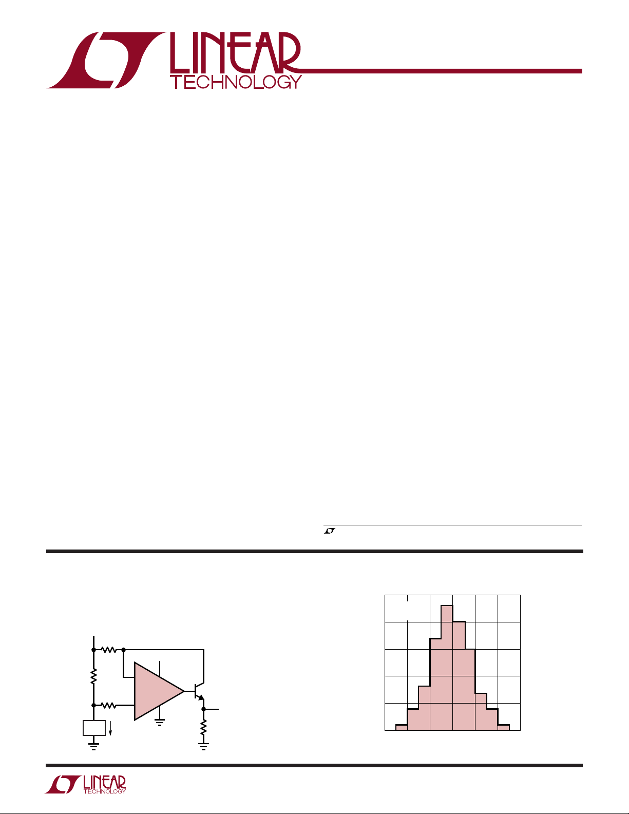
–900 –600 –300 0 300 600 900
PERCENTAGE OF AMPLIFIERS
INPUT OFFSET VOLTAGE (µV)
1782 G25
25
20
15
10
5
0
VS = 5V, 0V
V
CM
= 2.5V
LT1783
1.25MHz, Over-The-Top
Micropower, Rail-to-Rail
Input and Output Op Amp in SOT-23
U
DESCRIPTIO
■
Operates with Inputs Above V
■
Rail-to-Rail Input and Output
■
Micropower: 300µA Supply Current Max
■
Small SOT-23 Package
■
Gain Bandwidth product: 1.25MHz
■
Slew Rate: 0.42V/µs
■
Low Input Offset Voltage: 800µV Max
■
Single Supply Input Range: 0V to 18V
■
High Output Current: 18mA Min
■
Specified on 3V, 5V and ±5V Supplies
■
Output Shutdown on 6-Lead Version
■
Reverse Battery Protection to 18V
■
High Voltage Gain: 1500V/mV
■
Operating Temperature Range: –40°C to 85°C
+
U
APPLICATIO S
■
Portable Instrumentation
■
Battery- or Solar-Powered Systems
■
Sensor Conditioning
■
Supply Current Sensing
■
Battery Monitoring
■
MUX Amplifiers
■
4mA to 20mA Transmitters
The LT®1783 is a 1.25MHz op amp available in the small
SOT-23 package that operates on all single and split
supplies with a total voltage of 2.5V to 18V. The amplifier
draws less than 300µA of quiescent current and has
reverse battery protection, drawing negligible current for
reverse supply voltages up to 18V.
The input range of the LT1783 includes ground, and a
unique feature of this device is its Over-The-TopTM operation capabilitity with either or both of its inputs above the
positive rail. The inputs handle 18V both differential and
common mode, independent of supply voltage. The input
stage incorporates phase reversal protection to prevent
false outputs from occurring even when the inputs are 9V
below the negative supply.
The LT1783 can drive loads up to 18mA and still maintain
rail-to-rail capability. A shutdown feature on the 6-lead
version can disable the part, making the output high
impedance and reducing quiescent current to 5µA. The
LT1783 op amp is available in the 5- and 6-lead
SOT-23 packages. For applications requiring lower power,
refer to the LT1782.
, LTC and LT are registered trademarks of Linear Technology Corporation.
Over-The-Top is a trademark of Linear Technology Corporation.
TYPICAL APPLICATIO
Positive Supply Rail Current Sense
+
V
5V TO 18V
LOAD
200Ω
0.2Ω
200Ω
I
LOAD
+
LT1783
–
U
Distribution of Input Offset Voltage
5V
2N3904
V
0V TO 4.3V
2k
OUT
1783 TA01
= 2Ω(I
LOAD
)
1
LT1783
WW
W
ABSOLUTE MAXIMUM RATINGS
Total Supply Voltage (V+ to V–) .............................. 18V
Input Differential Voltage ........................................ 18V
Input Pin Voltage to V–............................... +24V/– 10V
Shutdown Pin Voltage Above V–............................ 18V
Shutdown Pin Current ....................................... ±10mA
U
(Note 1)
Operating Temperature Range (Note 10) –40°C to 85°C
Specified Temperature Range ......................
Junction Temperature........................................... 150°C
Storage Temperature Range ................ –65°C to 150°C
Lead Temperature (Soldering, 10 sec)................. 300°C
Output Short-Circuit Duration (Note 2) ........... Indefinite
U
W
U
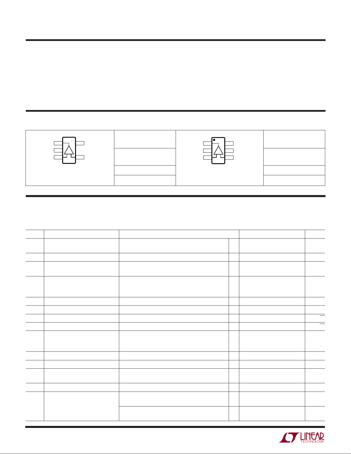
PACKAGE/ORDER INFORMATION
TOP VIEW
+
1
OUT
–
2
V
+IN
T
JMAX
Consult factory for Industrial and Military grade parts.
+
3
S5 PACKAGE
5-LEAD PLASTIC SOT-23
= 150°C, θJA = 250°C/ W
5
V
–
–IN
4
ORDER PART
LT1783CS5
S5 PART MARKING S6 PART MARKING
NUMBER
LTLF
OUT
+IN
TOP VIEW
1
–
2
V
6-LEAD PLASTIC SOT-23
T
JMAX
+
3
–
S6 PACKAGE
= 150°C, θJA = 230°C/ W
+
ORDER PART
V
6
SHDN
5
–IN
4
NUMBER
LT1783CS6
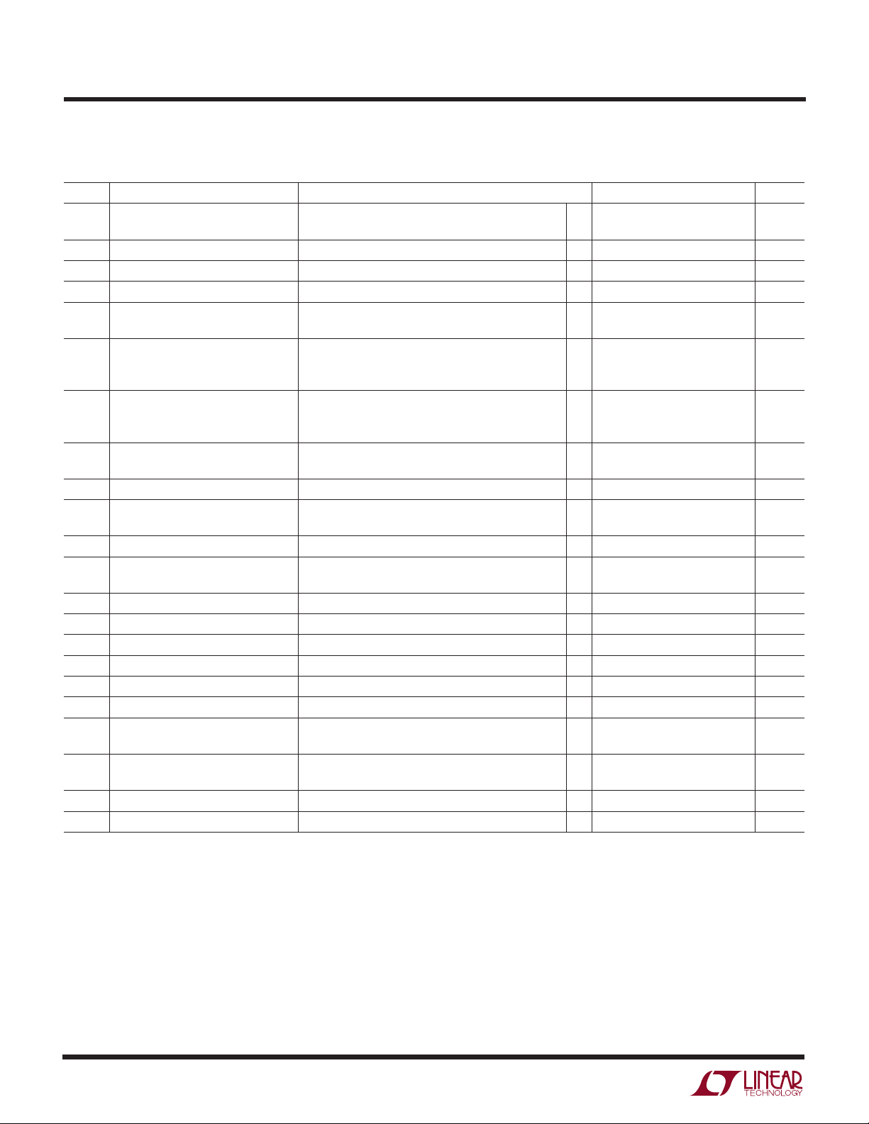
ELECTRICAL CHARACTERISTICS
The ● denotes specifications which apply over the specified temperature range, otherwise specifications are TA = 25°C.
VS = 3V, 0V; VS = 5V, 0V, VCM = V
= half supply, for the 6-lead part V
OUT
= 0V, pulse power tested unless otherwise specified.
PIN5
0°C to 70°C
LTIU
SYMBOL PARAMETER CONDITIONS MIN TYP MAX UNITS
V
OS
I
OS
I
B
e
n
i
n
R
IN
C
IN
CMRR Common Mode Rejection Ratio VCM = 0V to VCC – 1V ● 90 100 dB
PSRR Power Supply Rejection Ratio VS = 3V to 12.5V, VCM = VO = 1V ● 90 100 dB
A
VOL
Input Offset Voltage T
Input Offset Voltage Drift (Note 7) 0°C ≤ TA ≤ 70°C ● 25µV/°C
Input Offset Current ● 48 nA
Input Bias Current ● 45 80 nA
Input Bias Current Drift 0°C ≤ TA ≤ 70°C ● 0.06 nA/°C
Input Noise Voltage 0.1Hz to 10Hz 0.6 µV
Input Noise Voltage Density f = 1kHz 20 nV/√Hz
Input Noise Current Density f = 1kHz 0.14 pA/√Hz
Input Resistance Differential 0.65 1.3 MΩ
Input Capacitance 5pF
Input Voltage Range ● 018V
(Note 3) V
Large-Signal Voltage Gain VS = 3V, VO = 500mV to 2.5V, RL = 10k 200 1500 V/mV
= 25°C 400 800 µV
A
≤ 70°C ● 950 µV
0°C ≤ T
A
= 18V (Note 3) ● 7 µA
V
CM
V
= 18V (Note 3) ● 35 60 µA
CM
SHDN or V
Common Mode, V
Common Mode, V
CM
V
= 3V, 0°C ≤ TA ≤ 70°C ● 133 V/mV
S
VS = 5V, VO = 500mV to 4.5V, RL = 10k 400 1500 V/mV
V
= 5V, 0°C ≤ TA ≤ 70°C ● 250 V/mV
S
= 0V, VCM = 0V to 18V 0.1 nA
S
P-P
= 0V to (V
CM
= 0V to 18V 0.3 0.5 MΩ
CM
= 0V to 18V (Note 6) ● 68 80 dB
– 1V) 1 GΩ
CC
2

LT1783
ELECTRICAL CHARACTERISTICS
The ● denotes specifications which apply over the specified temperature range, otherwise specifications are TA = 25°C.
VS = 3V, 0V; VS = 5V, 0V, VCM = V
SYMBOL PARAMETER CONDITIONS MIN TYP MAX UNITS
V
OL
V
OH
I
SC
I
S
I
SHDN
V
L
V
H
t
ON
t
OFF
GBW Gain Bandwidth Product f = 5kHz 750 1250 kHz
SR Slew Rate AV = –1, R
FPBW Full-Power Bandwidth (Note 9) V
t
S
THD Distortion VS = 3V, VO = 2V
Output Voltage Swing LOW No Load ● 38 mV
Output Voltage Swing HIGH VS = 3V, No Load ● 2.91 2.94 V
Short-Circuit Current (Note 2) VS = 3V, Short to GND 5 10 mA
Minimum Supply Voltage ● 2.5 2.7 V
Reverse Supply Voltage I
Supply Current 210 300 µA
(Note 4)
Supply Current, SHDN V
Shutdown Pin Current V
Shutdown Output Leakage Current V
Maximum Shutdown Pin Current V
Shutdown Pin Input Low Voltage (Note 8) ● 0.3 V
Shutdown Pin Input High Voltage (Note 8) ● 2V
Turn-On Time V
Turn-Off Time V
(Note 3) 0°C ≤ T
(Note 5) 0°C ≤ T
Settling Time V
= half supply, for the 6-lead part V
OUT
= 5mA ● 200 400 mV
I
SINK
V
= 5V, I
S
= 3V, I
V
S
= 10mA ● 330 600 mV
SINK
= 5mA ● 2.6 2.8 V
SOURCE
VS = 5V, No Load ● 4.91 4.94 V
= 5V, I
V
S
V
= 3V, Short to V
S
= 10mA ● 4.5 4.74 V
SOURCE
CC
VS = 5V, Short to GND 15 30 mA
V
= 5V, Short to V
S
= –100µA ● 18 V
S
= 2V, No Load (Note 8) ● 518 µA
PIN5
= 0.3V, No load (Note 8) ● 0.5 nA
PIN5
= 2V, No Load (Note 8) ● 28 µA
V
PIN5
= 5V, No Load (Note 8) 5 µA
V
PIN5
= 2V, No Load (Note 8) ● 0.05 1 µA
PIN5
= 18V, No Load (Note 8) ● 10 30 µA
PIN5
= 5V to 0V, R
PIN5
= 0V to 5V, R
PIN5
≤ 70°C ● 600 kHz
A
≤ 70°C ● 0.21 V/µs
A
= 2V
OUT
P-P
= 5V, ∆V
S
CC
= 10k (Note 8) 25 µs
L
= 10k (Note 8) 3 µs
L
= ∞ 0.24 0.42 V/µs
L
= 2V to 0.1%, A
OUT
, AV = 1, RL = 10k, f = 1kHz 0.001 %
P-P
= 0V, pulse power tested unless otherwise specified.
PIN5
15 30 mA
20 40 mA
● 350 µA
66 kHz
= –1 12 µs
V
V
= ±5V, V
S
V
OS
I
OS
I
B
e
n
i
n
= 0V,V
CM
= 0V, for the 6-lead part V
OUT
Input Offset Voltage T
SHDN
= 25°C 500 900 µV
A
0°C ≤ T
≤ 70°C ● 1050 µV
A
= V
–
Input Offset Voltage Drift (Note 7) 0°C ≤ TA ≤ 70°C ● 25µV/°C
Input Offset Current ● 48 nA
Input Bias Current ● 40 80 nA
Input Bias Current Drift 0°C ≤ TA ≤ 70°C ● 0.06 nA/°C
Input Noise Voltage 0.1Hz to 10Hz 1 µV
P-P
Input Noise Voltage Density f = 1kHz 20 nV/√Hz
Input Noise Current Density f = 1kHz 0.14 pA/√Hz
3
LT1783
ELECTRICAL CHARACTERISTICS
The ● denotes specifications which apply over the specified temperature range, otherwise specifications are TA = 25°C.
V
= ±5V, V
S
SYMBOL PARAMETER CONDITIONS MIN TYP MAX UNITS
R
IN
C
IN
CMRR Common Mode Rejection Ratio VCM = –5V to 13V ● 68 80 dB
A
VOL
V
OL
V
OH
I
SC
PSRR Power Supply Rejection Ratio V
I
S
I
SHDN
V
L
V
H
t
ON
t
OFF
GBW Gain Bandwidth Product f = 5kHz 800 1300 kHz
SR Slew Rate AV = –1, R
FPBW Full-Power Bandwidth (Note 9) V
t
S
Note 1: Absolute Maximum Ratings are those values beyond which the life
of a device may be impaired.
Note 2: A heat sink may be required to keep the junction temperature
below absolute maximum.
Note 3: V
= ±5V or VS = ±9V tests.
V
S
Note 4: VS = 3V limits are guaranteed by correlation to VS = 5V and
= ±5V or VS = ±9V tests.
V
S
Note 5: Guaranteed by correlation to slew rate at V
= 3V and V
V
S
= 0V,V
CM
= 0V, for the 6-lead part V
OUT
= V–, unless otherwise specified.
SHDN
Input Resistance Differential ● 0.65 1.3 MΩ
Common Mode, V
= –5V to 13V ● 0.3 0.5 MΩ
CM
Input Capacitance 5pF
Input Voltage Range ● –5 13 V
Large-Signal Voltage Gain V
= ±4V, R
O
0°C ≤ T
= 10k 70 160 V/mV
L
≤ 70°C ● 50 V/mV
A
Output Voltage Swing LOW No Load ● –4.997 –4.992 V
= 5mA ● –4.8 –4.6 V
I
SINK
= 10mA ● –4.67 –4.4 V
I
SINK
Output Voltage Swing HIGH No Load ● 4.91 4.94 V
I
= 5mA ● 4.6 4.8 V
SOURCE
= 10mA ● 4.5 4.74 V
I
SOURCE
Short-Circuit Current (Note 2) Short to GND 18 30 mA
≤ 70°C ● 15 mA
0°C ≤ T
A
= ±1.5V to ±9V ● 90 100 dB
S
Supply Current 230 325 µA
● 375 µA
Supply Current, SHDN V
Shutdown Pin Current V
Maximum Shutdown Pin Current V
Shutdown Output Leakage Current V
Shutdown Pin Input Low Voltage V
Shutdown Pin Input High Voltage V
Turn-On Time V
Turn-Off Time V
Settling Time ∆V
= –3V, V
PIN5
= –4.7V, V
PIN5
V
= –3V, V
PIN5
= 9V, V
PIN5
= –7V, V
PIN5
= ±5V (Note 8) ● –4.7 V
S
= ±5V (Note 8) ● –2.8 V
S
= 0V to –5V, R
PIN5
= –5V to 0V, R
PIN5
0°C ≤ T
0°C ≤ T
= 8V
OUT
= 4V to 0.1%, A
OUT
= ±5V, No Load (Note 8) ● 620 µA
S
= ±5V, No load (Note 8) ● 0.5 nA
S
= ±5V, No Load (Note 8) ● 28 µA
S
= ±9V (Note 8) ● 10 30 µA
S
= ±9V, No Load (Note 8) ● 0.05 1 µA
S
= 10k (Note 8) ● 25 µs
L
= 10k (Note 8) ● 3 µs
L
≤ 70°C ● 700 kHz
A
= ∞, VO = ±4V, Measured at VO = ±2V 0.26 0.45 V/µs
L
≤ 70°C ● 0.23 V/µs
A
P-P
= 1 10 µs
V
18 kHz
Note 6: This specification implies a typical input offset voltage of 1.8mV at
= 18V and a maximum input offset voltage of 7.2mV at VCM = 18V.
V
CM
Note 7: This parameter is not 100% tested.
Note 8: Specifications apply to 6-lead SOT-23 with shutdown.
= 5V limits are guaranteed by correlation to VS = 3V and
S
Note 9: Full-power bandwidth is calculated from the slew rate.
FPBW = SR/2πV
.
P
Note 10: The LT1783 is guaranteed functional over the operating
temperature range –40°C to 85°C.
= ±5V, and GBW at
= ±5V tests.
S
S
4
 Loading...