

Linear Technology LT1777 Datasheet
FEATURES
LT1777
Low Noise Step-Down
Switching Regulator
U
DESCRIPTIO
■
Programmable dI/dt Limit
■
Internally Limited dV/dt
■
High Input Voltage: 48V Max
■
700mA Peak Switch Rating
■
True Current Mode Control
■
100kHz Fixed Operating Frequency
■
Synchronizable to 250kHz
■
Low Supply Current in Shutdown: 30µA
■
Low Thermal Resistance 16-Pin SO Package
U
APPLICATIO S
■
Automotive Cellular and GPS Receivers
■
Telecom Power Supplies
■
Industrial Instrument Power Supplies
U
TYPICAL APPLICATIO
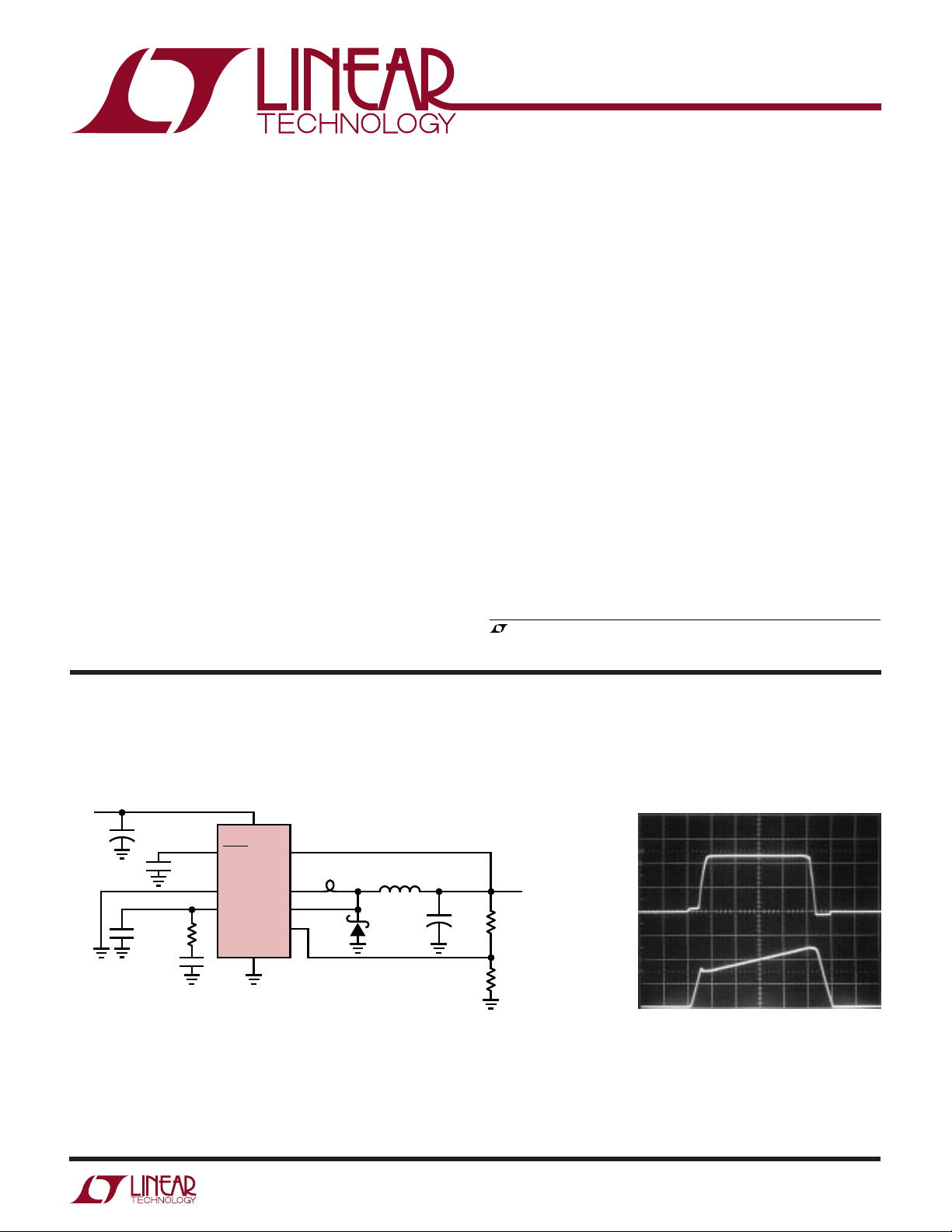
The LT®1777 is a Buck (step-down) regulator designed for
noise sensitive applications. It contains a dI/dt limiting
circuit programmed via a small external inductor in the
switching path. Internal circuitry also generates controlled
dV/dt ramp rates.
The monolithic die includes all oscillator, control and
protection circuitry. The part can accept operating input
voltages as high as 48V, and contains an output switch
rated at 700mA peak current. Current mode control offers
excellent dynamic input supply rejection and short-circuit
protection. The internal control circuitry is normally powered via the VCC pin, thereby minimizing power drawn
directly from the VIN supply (see Applications Information). The fused-lead SO16 package and 100kHz switching frequency allow for minimal PC board area
requirements.
, LTC and LT are registered trademarks of Linear Technology Corporation.
V
IN
24V
+
*PROGRAMS dI/dT
39µF
63V
100pF
2200pF
100pF
12k
VSW Switching WaveformsLow Noise 5V Step-Down Supply
10
V
IN
3
SHDN
LT1777
12
SYNC
14
V
C
SGND
4
V
CC
1µH*
6
V
SW
5
V
D
13
FB
7
220µH
MBRS1100
V
OUT
5V
+
100µF
10V
36.5k
1%
12.1k
1%
1777 TA01
400mA
V
SW
VOLTAGE
10V/DIV
V
SW
CURRENT
200mA/DIV
500ns/DIV
1777 TA02
1
LT1777
TOP VIEW
S PACKAGE
16-LEAD PLASTIC SO
1
2
3
4
5
6
7
8
16
15
14
13
12
11
10
9
GND*
NC
SHDN
V
CC
V
D
V
SW
SGND
GND*
GND*
NC
V
C
FB
SYNC
NC
V
IN
GND*
WW
W
ABSOLUTE MAXIMUM RATINGS
U
PACKAGE
/
O
RDER I FOR ATIO
WU
(Note 1)
Supply Voltage ....................................................... 48V
Switch Voltage (VIN – VSW) (Note 4) ...................... 51V
ORDER PART
NUMBER
SHDN, SYNC Pin Voltage.......................................... 7V
VCC Pin Voltage ...................................................... 30V
FB Pin Voltage ........................................................ 3.0V
LT1777CS
LT1777IS
Operating Junction Temperature Range
LT1777C............................................... 0°C to 125°C
LT1777I ........................................... –40°C to 125°C
Storage Temperature Range ................ –65°C to 150°C
Lead Temperature (Soldering, 10 sec)................. 300°C
T
= 125°C, θJA = 50°C/W*
JMAX
Consult factory for Military grade parts.
*FOUR CORNER PINS ARE
FUSED TO INTERNAL DIE
ATTACH PADDLE FOR HEAT
SINKING. CONNECT THESE
FOUR PINS TO EXPANDED PC
LANDS FOR PROPER HEAT
SINKING.
ELECTRICAL CHARACTERISTICS
The ● denotes specifications which apply over the full operating temperature range, otherwise specifications are at TJ = 25°C.
VIN = 24V, VSW Open, VCC = 5V, VC = 1.4V unless otherwise noted.
U
SYMBOL PARAMETER CONDITIONS MIN TYP MAX UNITS
Power Supplies
V
IN(MIN)
I
VIN
I
VCC
V
VCC
Feedback Amplifier
V
REF
I
IN
g
m
I
, I
SRC
V
CL
2
Minimum Input Voltage 6.7 7.0 V
● 7.4 V
VIN Supply Current VC = 0V 620 800 µA
● 900 µA
VCC Supply Current VC = 0V 2.5 3.5 mA
● 4.5 mA
VCC Dropout Voltage (Note 2) ● 2.8 3.1 V
Shutdown Mode I
Reference Voltage 1.225 1.240 1.255 V
FB Pin Input Bias Current 600 1500 nA
Feedback Amplifier Transconductance ∆IC = ±10µA 400 650 1000 µmho
Feedback Amplifier Source or Sink Current 60 100 170 µA
SNK
Feedback Amplifier Clamp Voltage 2.0 V
Reference Voltage Line Regulation 12V ≤ VIN ≤ 48V ● 0.01 %/V
Voltage Gain 200 600 V/V
VIN
V
= 0V 30 50 µA
SHDN
● 75 µA
● 1.215 1.265 V
● 200 1500 µmho
● 45 220 µA
LT1777
ELECTRICAL CHARACTERISTICS
The ● denotes specifications which apply over the full operating temperature range, otherwise specifications are at TJ = 25°C.
VIN = 24V, VSW Open, VCC = 5V, VC = 1.4V unless otherwise noted.
SYMBOL PARAMETER CONDITIONS MIN TYP MAX UNITS
Output Switch
R
ON
I
LIM
Current Amplifier
Timing
f Switching Frequency 90 100 110 kHz
Sync Function
SHDN Pin Function
V
SHDN
I
SHDN
Output Switch On Voltage ISW = 0.5A 1.0 1.5 V
Switch Current Limit (Note 3) ● 0.55 0.70 1.0 A
Output dl/dt Sense Voltage 1.3 V
● 0.6 2.0 V
Control Pin Threshold Duty Cycle = 0% 0.9 1.1 1.25 V
Control Voltage to Switch Transconductance 2 A/V
● 85 115 kHz
Maximum Switch Duty Cycle ● 85 90 %
Minimum Sync Amplitude ● 1.5 2.2 V
Synchronization Range ● 130 250 kHz
SYNC Pin Input R 40 kΩ
Shutdown Mode Threshold 0.5 V
● 0.2 0.8 V
Upper Lockout Threshold Switching Action On 1.260 V
Lower Lockout Threshold Switching Action Off 1.245 V
Shutdown Pin Current V
= 0V 12 20 µA
SHDN
V
= 1.25V 2.5 10 µA
SHDN
Note 1: Absolute Maximum Ratings are those values beyond which the life
of a device may be impaired.
Note 2: Control circuitry powered from V
Note 3: Switch current limit is DC trimmed and tested in production.
Inductor dI/dt rate will cause a somewhat higher current limit in actual
application.
CC
.
Note 4: During normal operation the V
below ground. However, the LT1777 may not be used in an inverting
DC/DC configuration.
pin may fly as much as 3V
SW
3
LT1777
UW
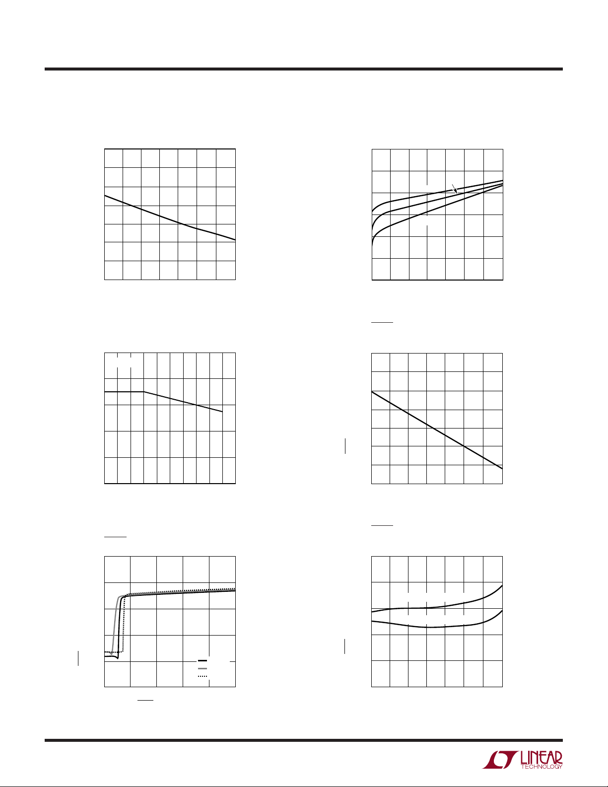
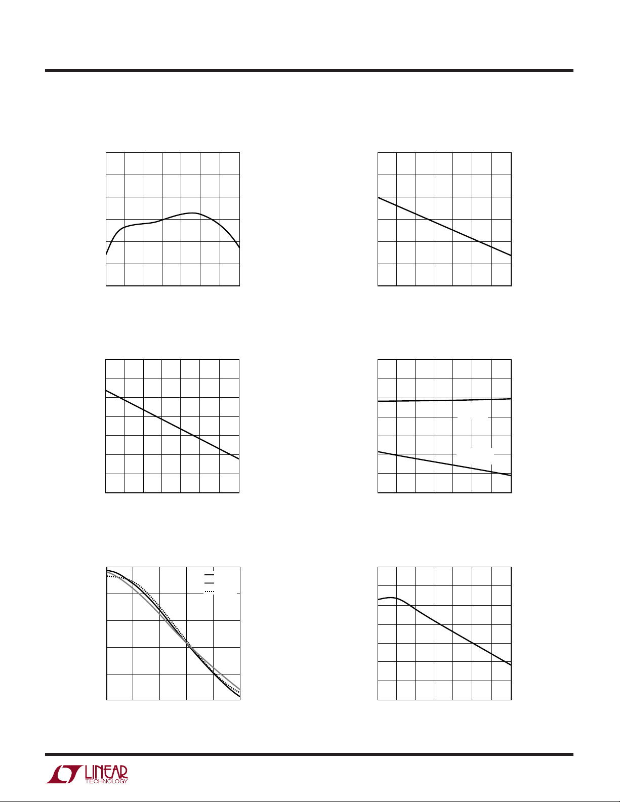
TYPICAL PERFOR A CE CHARACTERISTICS
Minimum Input Voltage
vs Temperature
7.4
7.2
7.0
6.8
6.6
INPUT VOLTAGE (V)
6.4
6.2
6.0
–50
–25 0
TEMPERATURE (°C)
Switch Current Limit
vs Duty Cycle
1000
TA = 25°C
800
600
50 100 125
25 75
1777 G01
Switch On Voltage
vs Switch Current
1.50
1.25
1.00
0.75
0.50
SWITCH VOLTAGE (V)
0.25
0
0
100 200
SWITCH CURRENT (mA)
–55°C
125°C
25°C
400 600 700
300 500
SHDN Pin Shutdown Threshold
vs Temperature
900
800
700
600
1777 G02
400
200
SWITCH CURRENT LIMIT (mA)
0
2010 30 50 70 90
0
40
DUTY CYCLE (%)
SHDN Pin Current vs Voltage
5
0
–5
–10
–15
SHDN PIN INPUT CURRENT (µA)
–20
1
0
2
SHDN PIN VOLTAGE (V)
500
400
SHDN PIN VOLTAGE (mV)
300
60
80
100
1777 G03
200
–50
–25 0
50 100 125
25 75
TEMPERATURE (°C)
1777 G04
SHDN Pin Lockout Thresholds
vs Temperature
1.30
1.28
UPPER THRESHOLD
1.26
LOWER THRESHOLD
1.24
25°C
125°C
–55°C
3
4
5
1777 G05
SHDN PIN VOLTAGE (V)
1.22
1.20
–50
–25 0
TEMPERATURE (°C)
50 100 125
25 75
1777 G06
4
UW
TYPICAL PERFOR A CE CHARACTERISTICS
LT1777
Switching Frequency
vs Temperature
106
104
102
100
98
SWITCHING FREQUENCY (kHz)
96
94
–50 25 75
–25 0
TEMPERATURE (°C)
Output dI/dt Sense Voltage
vs Temperature
2.0
1.8
1.6
1.4
50 100 125
1777 G07
Minimum Synchronization
Voltage vs Temperature
2.25
2.00
1.75
1.50
1.25
1.00
MINIMUM SYNCHRONIZATION VOLTAGE (V)
0.75
–50 25 75
–25 0
TEMPERATURE (°C)
50 100 125
VC Pin Switching Threshold,
Clamp Voltage vs Temperature
2.2
2.0
1.8
1.6
CLAMP
VOLTAGE
1777 G08
1.2
1.0
dI/dt SENSE VOLTAGE (V)
0.8
0.6
–50 25 75
–25 0
TEMPERATURE (°C)
Feedback Amplifier Output
Current vs FB Pin Voltage
100
50
0
–50
–100
FEEDBACK AMPLIFIER OUTPUT CURRENT (µA)
–150
1.0
1.1
1.2
FB PIN VOLTAGE (V)
50 100 125
1777 G09
25°C
125°C
–55°C
1.3
1.4
1777 G11
1.5
1.4
PIN VOLTAGE (V)
C
V
1.2
1.0
0.8
–50
–25 0
TEMPERATURE (°C)
SWITCHING
THRESHOLD
50 100 125
25 75
Error Amplifier Transconductance
vs Temperature
750
700
650
600
550
500
TRANSCONDUCTANCE (µmho)
450
400
–50
–25 0
TEMPERATURE (°C)
50 100 125
25 75
1777 G10
1777 G12
5
LT1777
PIN FUNCTIONS
UUU
GND (Pins 1, 8, 9, 16): These corner package pins are
mechanically connected to the die paddle and thus aid in
conducting away internally generated heat. As these are
electrically connected to the die substrate, they must be
held at ground potential. A direct connection to the local
ground plane is recommended.
NC (Pins 2, 11, 15): Package Pins 2, 11 and 15 are
unconnected.
SHDN (Pin 3): When pulled below the shutdown mode
threshold, nominally 0.5V, this pin turns off the regulator
and reduces VIN input current to a few tens of microamperes (shutdown mode).
When this pin is held above the shutdown mode threshold,
but below the lockout threshold, the part will be operational with the exception that output switching action will
be inhibited (lockout mode). A user-adjustable undervoltage lockout can be implemented by driving this pin from
an external resistor divider to VIN. This action is logically
“ANDed” with the internal UVLO, nominally set at 6.7V,
such that minimum VIN can be increased above 6.7V, but
not decreased (see Applications Information).
If unused, this pin should be left open. However, the high
impedance nature of this pin renders it susceptible to
coupling from the VSW node, so a small capacitor to
ground, typically 100pF or so is recommended when the
pin is left open.
VCC: (Pin 4): Pin to power the internal control circuitry
from the switching supply output. Proper use of this pin
enhances overall power supply efficiency. During start-up
conditions, internal control circuitry is powered directly
from VIN. If the output capacitor is located more than an
inch from the VCC pin, a separate 0.1µF bypass capacitor
to ground may be required right at the pin.
VD (Pin 5): This pin is used in conjunction with a small
external sense inductor to limit power path dI/dt. The
sense inductor is placed between the VSW output node and
the cathode of the freewheeling (power) diode, and the V
pin is connected to the diode. As the voltage across the
inductor reaches ±2VBE, drive to the output transistor is
D
removed or supplied accordingly to limit dI/dt (see Applications Information).
VSW (Pin 6): This is the emitter node of the output switch
and has large currents flowing through it. Keep the traces
to the switching components as short as possible to
minimize electromagnetic radiation and voltage spikes.
SGND (Pin 7): This is the device signal ground pin. The
internal reference and feedback amplifier are referred to it.
Keep the ground path connection to the FB divider and the
VC compensation capacitor free of large ground currents.
VIN (Pin 10): This is the high voltage supply pin for the
output switch. It also supplies power to the internal control
circuitry during start-up conditions or if the VCC pin is left
open. A high quality bypass capacitor which meets the
input ripple current requirements is needed here (see
Applications Information).
SYNC (Pin 12): Pin to synchronize internal oscillator to
external frequency reference. It is directly logic compatible and can be driven with any signal between 10% and
90% duty cycle. The sync function is internally disabled if
the FB pin voltage is low enough to cause oscillator
slowdown. If unused, this pin should be grounded.
FB (Pin 13): This is the inverting input to the feedback
amplifier. The noninverting input of this amplifier is internally tied to the 1.24V reference. This pin also slows down
the frequency of the internal oscillator when its voltage is
abnormally low, e.g. 2/3 of normal or less. This feature
helps maintain proper short-circuit protection. Coupling
from high speed noise to this pin can cause irregular
operation. (See Switch Node Considerations section.)
VC (Pin 14): This is the control voltage pin which is the
output of the feedback amplifier and the input of the
current comparator. Frequency compensation of the overall loop is effected by placing a capacitor (or in most cases
a series R/C combination) between this node and ground.
Coupling from high speed noise to this pin can cause
irregular operation. (See Switch Node Considerations
section.)
6
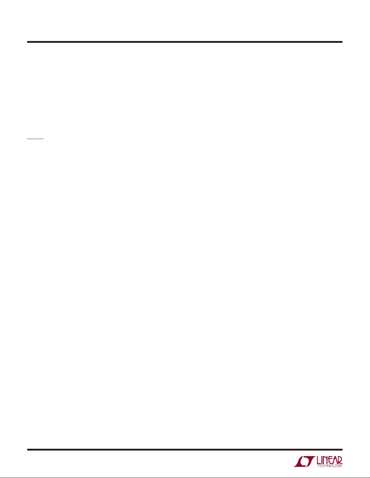
BLOCK DIAGRA
LT1777
W
V
CC
4
V
V
BG
LOGIC
FEEDBACK
AMP
g
m
B
SWDR
SWON
SHDN
3
SYNC
12
SGND
7
V
C
14
FB
13
OSC
V
BG
BIAS
R1
I
I
2
WW
OUTPUT STAGE SI PLIFIED SCHE ATIC
I
COMP
V
IN
10
R
SENSE
–dV/dt
LIMITER
Q2
Q1
V
SW
6
I
1
I
V
±dI/dt
LIMITER
1777 BD
D
5
V
C1
Q3Q2
R1
Q4
R2
Q6
Q1
I
1
SWITCH ON
I
SIGNAL
R3
Q5
R4
IN
L
V
SW
SENSE
L
MAIN
V
OUT
+
V
D
1777 SS
NOTE: R3 = R4
7

LT1777
OPERATIO
U
The LT1777 is a current mode step-down switcher regulator IC designed for low noise operation. The Block
Diagram shows an overall view of the system. The individual blocks are straightforward and similar to those
found in traditional designs, including: Internal Bias Regulator, Oscillator, Logic, and Feedback Amplifier. The novel
portion includes a specialized Output Switch section including circuits to limit the dI/dt and dV/dt switching rates.
The LT1777 operates much the same as traditional current
mode switchers, the major difference being its specialized
output switch section. Due to space constraints, this
discussion will not reiterate the basics of current mode
switcher/controllers and the “buck” topology. A good
source of information on these topics is Application Note
AN19.
A straightforward output stage is provided by current
source I1 driving the base of PNP transistor Q2. The
collector of Q2 in turn drives the base of NPN output device
Q1. The considerable base/collector capacitance of PNP
Q2 acts to limit dV/dt rate during switch turn-on. However,
when the switch is to be turned off, the only natural limit
to voltage slew rate would be the collector/base capacitance of Q1 providing drive for the same device. While
dependent upon output load level and Q1’s β, the turn-off
voltage slew rate would be typically much faster than the
turn-on rate. To limit the voltage slew rate on switch turnoff, an extra function is supplied. This is denoted by the
block labeled “–dV/dt Limiter.”
The details of the – dV/dt Limiter can be seen in the Output
Stage Simplified Schematic. Transistors Q3 and Q4 are
connected in a Darlington configuration whose input is
coupled with small-valued capacitor C1 to the VIN supply
rail. The product of negative voltage slew rate times this
capacitor value equals current, and when this current
through emitter/base resistor R1 exceeds a diode drop, Q3
and then Q4 turn on supplying base drive to output device
Q1 to limit –dV/dt rate.
In addition to voltage rates, the current slew rate also
needs to be controlled for reduced noise behavior. This is
provided by the section in the Block Diagram labeled
“±dI/dt Limiter.” The details of this circuit can be seen in
the Output Stage Simplified Schematic. Note that an extra,
small-valued inductor, termed the “sense inductor” has
been added to the classic buck topology. As this inductor
is external to the LT1777, its value can be chosen by the
user allowing for optimization on a per application basis.
Operation of the current slew limiter is as follows: The
product of the sense inductor times the dI/dt through it
generates a voltage according to the well known formula
V = (L)(dI/dt). The remainder of the circuit is configured
such that when the voltage across the sense inductor
reaches ±2VBE, drive current will be supplied or removed
as necessary to limit current slew rate. The actual sensing
is performed between the output node labeled VSW and a
new node labeled VD.
In the case of switch turn-on, current drive is provided by
PNP Q2. If the voltage at VSW reaches 2VBE above that at
VD, transistor Q5 turns on and removes a portion of Q2’s
drive from Q1’s base. Similarly for turn-off, as the V
node goes 2VBE below VD, transistor Q6 then turns on to
drive Q1’s base as needed. The net effect is that of limiting
the switch node dI/dt in both directions at a rate inversely
proportional to the external sense inductor value.
SW
8
 Loading...