

Linear Technology LT1776 Datasheet
FEATURES
■
Wide Input Range: 7.4V to 40V
■
Tolerates Input Transients to 60V
■
700mA Peak Switch Rating
■
Adaptive Switch Drive Maintains Efficiency at High
Load Without Pulse Skipping at Light Load
■
True Current Mode Control
■
200kHz Fixed Operating Frequency
■
Synchronizable to 400kHz
■
Low Supply Current in Shutdown: 30µA
■
Available in 8-Pin SO and PDIP Packages
U
APPLICATIO S
■
Automotive DC/DC Converters
■
Cellular Phone Battery Charger Accessories
■
IEEE 1394 Step-Down Converters
LT1776
Wide Input Range,
High Efficiency, Step-Down
Switching Regulator
U
DESCRIPTIO
The LT®1776 is a wide input range, high efficiency Buck
(step-down) switching regulator. The monolithic die includes all oscillator, control and protection circuitry. The
part can accept input voltages as high as 60V and contains
an output switch rated at 700mA peak current. Current
mode control delivers excellent dynamic input supply
rejection and short-circuit protection.
The LT1776 contains several features to enhance efficiency. The internal control circuitry is normally powered
via the VCC pin, thereby minimizing power drawn directly
from the VIN supply (see Applications Information). The
action of the LT1776 switch circuitry is also load dependent. At medium to high loads, the output switch circuitry
maintains fast rise time for good efficiency. At light loads,
rise time is deliberately reduced to avoid pulse skipping
behavior.
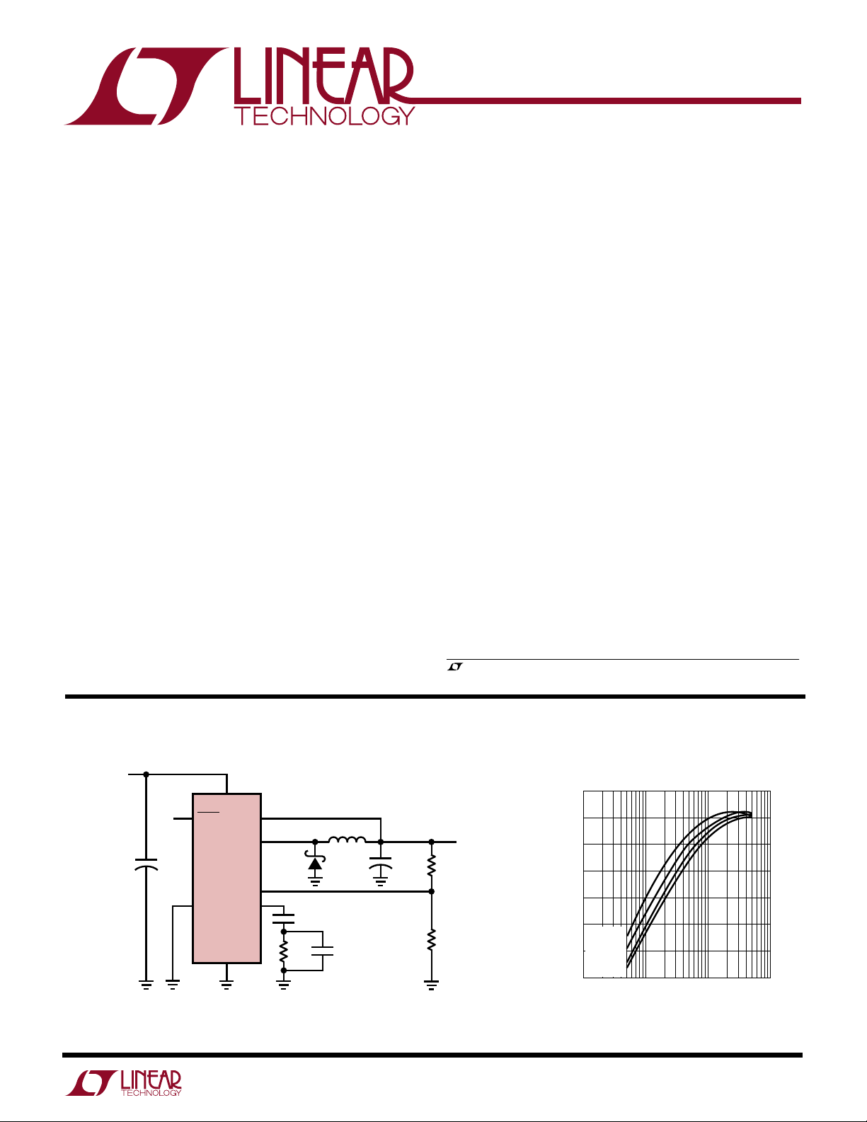
TYPICAL APPLICATIO
V
IN
8V TO 40V
1
+
39µF
63V
6
SHDN
SYNC
V
IN
LT1776
GND
5
4
V
CC
V
SW
FB
V
C
Figure 1
U
2
3
7
8
2200pF
22k
*43T #30 ON MAGNETICS
MPP #55030
100µH*
MBR160
100pF
The available SO-8 package and 200kHz switching frequency allow for minimal PC board area requirements.
, LTC and LT are registered trademarks of Linear Technology Corporation.
Efficiency vs VIN and I
90
80
5V
+
100µF
10V
36.5k
1%
12.1k
1%
1776 F01
400mA
70
60
50
EFFICIENCY (%)
40
VIN = 10V
V
= 20V
IN
30
VIN = 30V
V
= 40V
IN
20
1
10 100 1000
LOAD CURRENT (mA)
LOAD
1776 TA01
1
LT1776
1
2
3
4
8
7
6
5
TOP VIEW
V
C
FB
SYNC
V
IN
SHDN
V
CC
V
SW
GND
N8 PACKAGE
8-LEAD PDIP
S8 PACKAGE
8-LEAD PLASTIC SO
WW
W
ABSOLUTE MAXIMUM RA TIN GS
U
U
W
PACKAGE/ORDER INFORMA TION
(Note 1)
Supply Voltage (Note 5) .......................................... 60V
Switch Voltage (Note 5)........................................... 60V
SHDN, SYNC Pin Voltage........................................... 7V
VCC Pin Voltage ....................................................... 30V
FB Pin Voltage ........................................................... 3V
Operating Junction Temperature Range
LT1776C................................................0°C to 125°C
LT1776I............................................ –40°C to 125°C
Storage Temperature Range................. –65°C to 150°C
Lead Temperature (Soldering, 10 sec)..................300°C
T
= 125°C, θJA = 130°C/W (N8)
JMAX
T
= 125°C, θJA = 110°C/W (S8)
JMAX
Consult factory for Military grade parts.
ORDER PART
NUMBER
LT1776CN8
LT1776CS8
LT1776IN8
LT1776IS8
S8 PART MARKING
1776
1776I
ELECTRICAL CHARACTERISTICS
The ● denotes specifications which apply over the full operating temperature range, otherwise specifications are TA = 25°C.
VIN = 40V, VSW open, VCC = 5V, VC = 1.4V unless otherwise noted.
SYMBOL PARAMETER CONDITIONS MIN TYP MAX UNITS
Power Supplies
V
IN(MIN)
I
VIN
I
VCC
V
VCC
Feedback Amplifier
V
REF
I
IN
g
m
I
, I
SRC
V
CL
Output Switch
V
ON
I
LIM
Current Amplifier
2
Minimum Input Voltage 6.7 7.0 V
● 7.4 V
Thermally Limited Continuous Operating Voltage ● 40 V
VIN Supply Current VC = 0V 620 800 µA
● 900 µA
VCC Supply Current VC = 0V 3.2 4.0 mA
● 5.0 mA
VCC Dropout Voltage (Note 2) 2.8 3.1 V
Shutdown Mode I
Reference Voltage 1.225 1.240 1.255 V
FB Pin Input Bias Current 600 1500 nA
Feedback Amplifier Transconductance ∆lc = ±10µA 400 650 1000 µmho
Feedback Amplifier Source or Sink Current 60 100 170 µA
SNK
Feedback Amplifier Clamp Voltage 2.0 V
Reference Voltage Line Regulation 12V ≤ VIN ≤ 60V ● 0.01 %/V
Voltage Gain 200 600 V/V
Output Switch On Voltage ISW = 0.5A 1.0 1.5 V
Switch Current Limit (Note 3) ● 0.55 0.70 1.0 A
Control Pin Threshold Duty Cycle = 0% 0.9 1.1 1.25 V
Control Voltage to Switch Transconductance 2 A/V
VIN
V
= 0V 30 50 µA
SHDN
● 75 µA
● 1.215 1.265 V
● 200 1500 µmho
● 45 220 µA
U
LT1776
ELECTRICAL CHARACTERISTICS
The ● denotes specifications which apply over the full operating temperature range, otherwise specifications are TA = 25°C.
VIN = 40V, VSW open, VCC = 5V, VC = 1.4V unless otherwise noted.
SYMBOL PARAMETER CONDITIONS MIN TYP MAX UNITS
Timing
f Switching Frequency 180 200 220 kHz
● 170 230 kHz
Maximum Switch Duty Cycle ● 85 90 %
t
ON(MIN)
Boost Operation
Sync Function
SHDN Pin Function
V
SHDN
I
SHDN
Note 1: Absolute Maximum Ratings are those values beyond which the life
of a device may be impaired.
Note 2: Control circuitry powered from V
Note 3: Switch current limit is DC trimmed and tested in production.
Inductor dl/dt rate will cause a somewhat higher current limit in actual
application.
Note 4: Minimum switch on time is production tested with a 39Ω resistive
load to ground.
Minimum Switch On Time High dV/dt Mode, RL = 39Ω (Note 4) 300 ns
VC Pin Boost Threshold 1.35 V
dV/dt Below Threshold 0.2 V/ns
dV/dt Above Threshold 1.6 V/ns
Minimum Sync Amplitude ● 1.5 2.2 V
Synchronization Range (Note 6) ● 250 400 kHz
SYNC Pin Input R 40 kΩ
Shutdown Mode Threshold 0.5 V
● 0.2 0.8 V
Upper Lockout Threshold Switching Action On 1.260 V
Lower Lockout Threshold Switching Action Off 1.245 V
Shutdown Pin Current V
.
CC
= 0V 12 20 µA
SHDN
= 1.25V 2.5 10 µA
V
SHDN
Note 5: Parts are guaranteed to survive 60V on VIN and VSW. However,
thermal constraints will limit V
on maximum output current and switching frequency. See Applications
section for more information.
Note 6: Internal oscillator is guaranteed to sync up to 400kHz. However,
thermal constraints and/or controllability issues may place a lower limit on
switching frequency in actual usage. See Applications section for more
information.
in some applications, depending primarily
IN
3
LT1776
UW
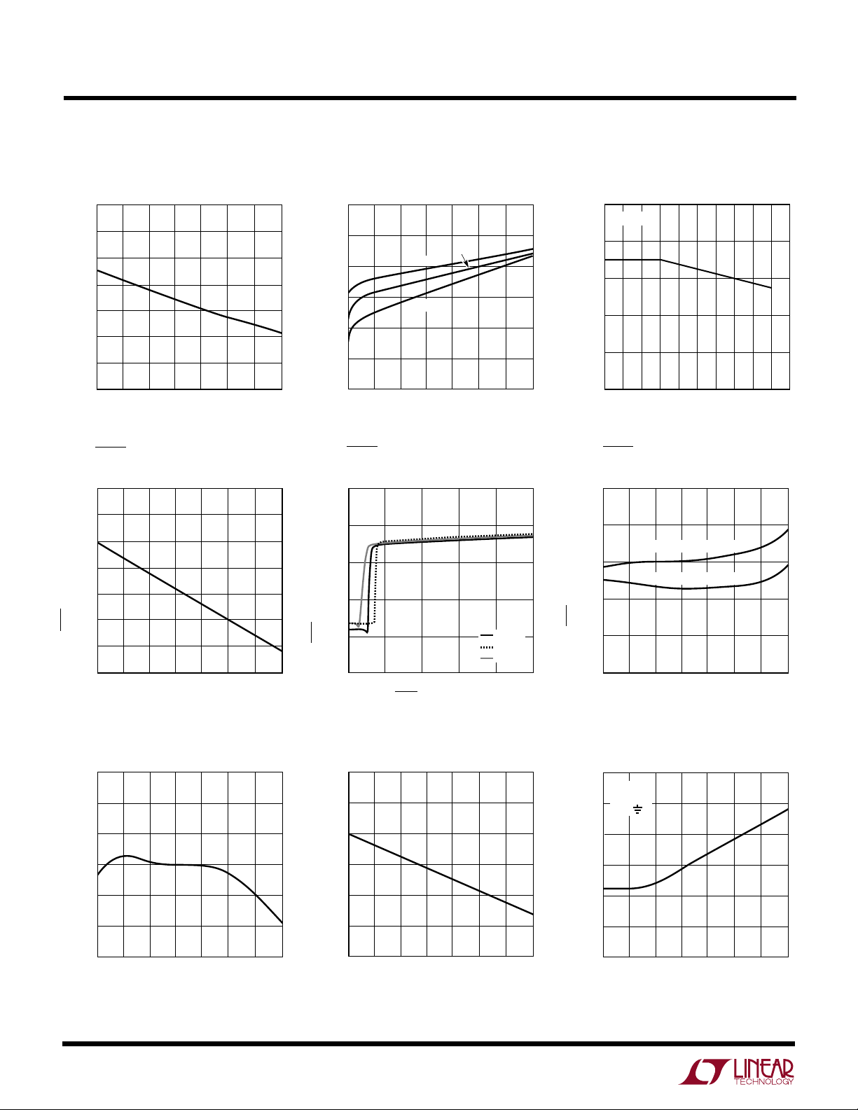
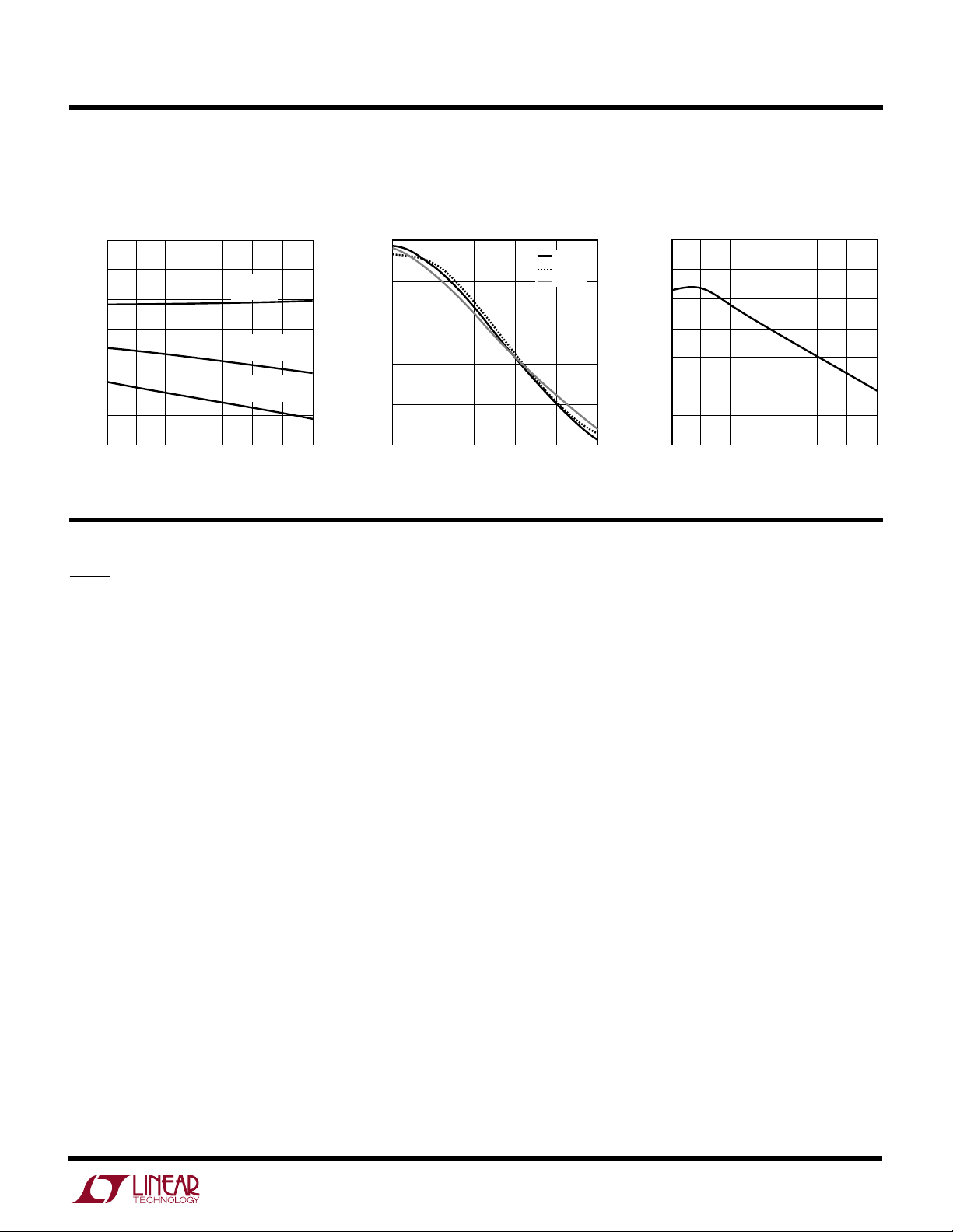
TYPICAL PERFORMANCE CHARACTERISTICS
Minimum Input Voltage vs
Temperature
7.4
7.2
7.0
6.8
6.6
INPUT VOLTAGE (V)
6.4
6.2
6.0
–50
–25 0
TEMPERATURE (°C)
50 100 125
25 75
SHDN Pin Shutdown Threshold
vs Temperature
900
800
700
600
500
400
SHDN PIN VOLTAGE (mV)
300
200
–50
–25 0
TEMPERATURE (°C)
50 100 125
25 75
1776 G01
LT1776 G04
Switch-On Voltage vs
Switch Current
1.50
1.25
1.00
0.75
0.50
SWITCH VOLTAGE (V)
0.25
0
0
–55°C
125°C
100 200
SWITCH CURRENT (mA)
SHDN Pin Input Current
vs Voltage
5
0
–5
–10
–15
SHDN PIN INPUT CURRENT (µA)
–20
1
0
SHDN PIN VOLTAGE (V)
25°C
400 600 700
300 500
3
2
25°C
–55°C
125°C
4
1776 G02
1776 G05
Switch Current Limit vs
Duty Cycle
1000
TA = 25°C
800
600
400
200
SWITCH CURRENT LIMIT (mA)
0
2010 30 50 70 90
0
DUTY CYCLE (%)
60
80
40
100
1776 G03
SHDN Pin Lockout Thresholds
vs Temperature
1.30
1.28
UPPER THRESHOLD
1.26
LOWER THRESHOLD
1.24
SHDN PIN VOLTAGE (V)
1.22
5
1.20
–50
–25 0
TEMPERATURE (°C)
50 100 125
25 75
LT1776 G06
Switching Frequency
vs Temperature
215
210
205
200
195
SWITCHING FREQUENCY (kHz)
190
185
–50 25 75
–25 0
TEMPERATURE (°C)
4
50 100 125
1776 G07
Minimum Synchronization Voltage
vs Temperature
2.25
2.00
1.75
1.50
1.25
1.00
MINIMUM SYNCHRONIZATION VOLTAGE (V)
0.75
–50 25 75
–25 0
TEMPERATURE (°C)
50 100 125
1776 G08
Switch Minimum On-Time
vs Temperature
600
V
= 40V
IN
= 39Ω
R
L
500
FB =
400
300
200
100
SWITCH MINIMUM ON-TIME (ns)
0
–50 25 75
–25 0
TEMPERATURE (°C)
50 100 125
1776 G09
UW
TYPICAL PERFORMANCE CHARACTERISTICS
VC Pin Switching Threshold,
Boost Threshold, Clamp Voltage
vs Temperature
2.2
2.0
1.8
1.6
1.4
PIN VOLTAGE (V)
C
V
1.2
1.0
0.8
–50
–25 0
25 75
TEMPERATURE (°C)
CLAMP
VOLTAGE
THRESHOLD
SWITCHING
THRESHOLD
50 100 125
BOOST
LT1776 G10
Feedback Amplifier Output
Current vs FB Pin Voltage
100
50
0
–50
–100
FEEDBACK AMPLIFIER OUTPUT CURRENT (µA)
–150
1.0
1.1
1.2
FB PIN VOLTAGE (V)
1.3
1.4
UUU
PIN FUNCTIONS
25°C
–55°C
125°C
1776 G11
1.5
LT1776
Error Amplifier Transconductance
vs Temperature
750
700
650
600
550
500
TRANSCONDUCTANCE (µmho)
450
400
–50
–25 0
TEMPERATURE (°C)
50 100 125
25 75
LT1776 G12
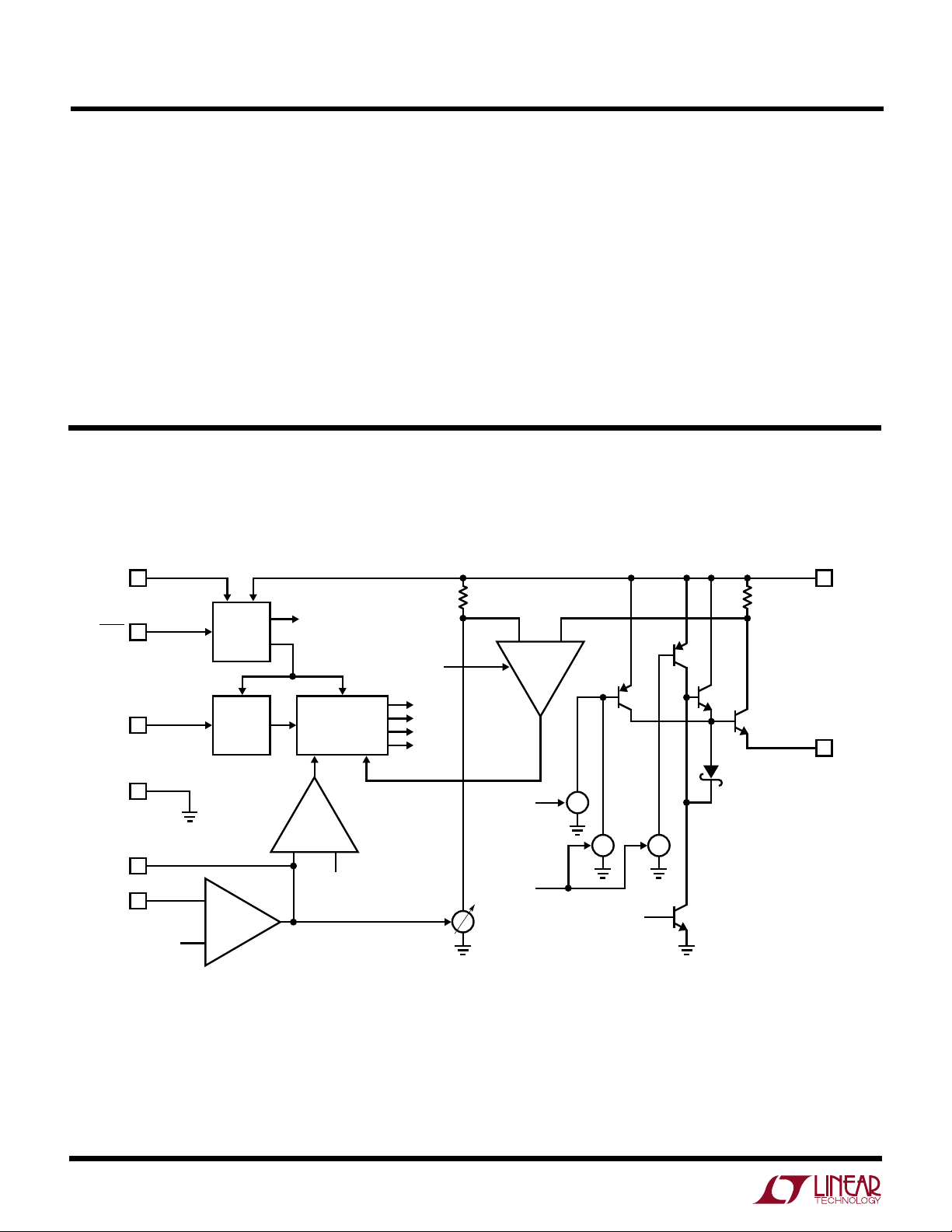
SHDN (Pin 1): When pulled below the shutdown mode
threshold, nominally 0.30V, this pin turns off the regulator
and reduces VIN input current to a few tens of microamperes (shutdown mode).
When this pin is held above the shutdown mode threshold,
but below the lockout threshold, the part will be operational with the exception that output switching action will
be inhibited (lockout mode). A user-adjustable undervoltage lockout can be implemented by driving this pin from
an external resistor divider to VIN. This action is logically
“ANDed” with the internal UVLO, set at nominally 6.7V,
such that minimum VIN can be increased above 6.7V, but
not decreased (see Applications Information).
If unused, this pin should be left open. However, the high
impedance nature of this pin renders it susceptible to
coupling from the high speed VSW node, so a small
capacitor to ground, typically 100pF or so is recommended when the pin is left “open”.
VCC (Pin 2): This pin is used to power the internal control
circuitry off of the switching supply output. Proper use of
this pin enhances overall power supply efficiency. During
start-up conditions, internal control circuitry is powered
directly from VIN.
If the output capacitor is located more than one inch from
the VCC pin, a separate 0.1µF bypass capacitor to ground
may be required right at the pin.
VSW (Pin 3): This is the emitter node of the output switch
and has large currents flowing through it. This node
moves at a high dV/dt rate, especially when in “boost”
mode. Keep the traces to the switching components as
short as possible to minimize electromagnetic radiation
and voltage spikes.
GND (Pin 4): This is the device ground pin. The internal
reference and feedback amplifier are referred to it. Keep
the ground path connection to the FB divider and the V
C
compensation capacitor free of large ground currents.
VIN (Pin 5): This is the high voltage supply pin for the
output switch. It also supplies power to the internal control
circuitry during start-up conditions or if the VCC pin is left
open. A high quality bypass capacitor which meets the
input ripple current requirements is needed here. (See
Applications Information).
SYNC (Pin 6): Pin used to synchronize internal oscillator
to the external frequency reference. It is directly logic
compatible and can be driven with any signal between
5
LT1776
SWDR
SWDR
SWON
SWON
BOOST
1776 BD
BOOST
SWOFF
SWOFF
LOGICOSC
BIAS
V
TH
V
B
V
BG
V
BG
FB
V
C
GND
SYNC
SHDN
V
CC
FB
AMP
BOOST
COMP
gm
I
I
I I
R1 R
SENSE
I
COMP
Q4
Q3
Q2
Q1
Q5
V
SW
D1
V
IN
5
3
2
1
6
4
8
7
UUU
PIN FUNCTIONS
10% and 90% duty cycle. The sync function is internally
disabled if the FB pin voltage is low enough to cause
oscillator slowdown. If unused, this pin should be grounded.
FB (Pin 7): This is the inverting input to the feedback
amplifier. The noninverting input of this amplifier is internally tied to the 1.24V reference. This pin also slows down
the frequency of the internal oscillator when its voltage is
W
BLOCK DIAGRA
abnormally low, e.g., 2/3 of normal or less. This feature
helps maintain proper short-circuit protection.
VC (Pin 8): This is the control voltage pin which is the
output of the feedback amplifier and the input of the
current comparator. Frequency compensation of the overall loop is effected by placing a capacitor, (or in most cases
a series RC combination) between this node and ground.
6
 Loading...