

Page 1

FEATURES
■
Wide Input Range: 3.6V to 25V
■
5V at 400mA from 7V to 25V Input
■
3.3V at 400mA from 4.7V to 25V Input
■
Fixed Frequency 1.4MHz Operation
■
Uses Tiny Capacitors and Inductors
■
Internally Compensated
■
Low Shutdown Current: <1µA
■
Low V
■
Tiny 6-Lead SOT-23 Package
Switch: 220mV at 300mA
CESAT
U
APPLICATIO S
■
Wall Transformer Regulation
■
Local Logic Supply Conversion:
12V to 5V
12V or 5V to 3.3V, 2.5V or 1.8V
■
Distributed Supply Regulation
■
Digital Cameras
■
Battery-Powered Equipment
LT1616
600mA, 1.4MHz Step-Down
Switching Regulator
in SOT-23
U
DESCRIPTIO
The LT®1616 is a current mode PWM step-down DC/DC
converter with internal 0.6A power switch, packaged in a
tiny 6-lead SOT-23. The wide input range of 3.6V to 25V
makes the LT1616 suitable for regulating a wide variety of
power sources, from 4-cell batteries and 5V logic rails to
unregulated wall transformers and lead-acid batteries. Its
high operating frequency allows the use of tiny, low cost
inductors and ceramic capacitors. With its internal compensation eliminating additional components, a complete
400mA step-down regulator fits onto 0.15 square inches
of PC board area.
The constant frequency current mode PWM architecture
and stable operation with ceramic capacitors results in
low, predictable output ripple. Current limiting provides
protection against shorted outputs. The low current (<1µ A)
shutdown provides complete output disconnect, enabling
easy power management in battery-powered systems.
, LTC and LT are registered trademarks of Linear Technology Corporation.
TYPICAL APPLICATIO
3.3V Step-Down Converter
V
4.5V TO 25V
OFF ON
IN
5
V
IN
LT1616
4
SHDN SW
GND FB
23
C1
1µF
C1: TAIYO-YUDEN TMK316BJ105
C2: TAIYO-YUDEN JMK316BJ106ML
D1: ON SEMICONDUCTOR MBR0530
D2: 1N4148
L1: SUMIDA CR43-100
BOOST
1
6
R1
16.5k
R2
10k
U
C3
0.01µF
D1
Efficiency
D2
L1
10µH
V
OUT
3.3V
300mA: V
400mA: V
C2
10µF
1616 TA01
= 4.5V TO 25V
IN
= 4.7V TO 25V
IN
100
90
80
70
60
EFFICIENCY (%)
50
40
30
0
VIN = 5V
100 200 500
LOAD CURRENT (mA)
VIN = 12V
VIN = 20V
300 400
1616 G02
1
Page 2
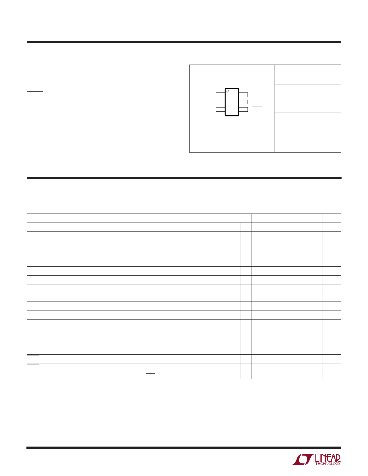
LT1616
PACKAGE/ORDER I FOR ATIO
UU
W
BOOST 1
GND 2
FB 3
6 SW
5 V
IN
4 SHDN
TOP VIEW
S6 PACKAGE
6-LEAD PLASTIC SOT-23
WWWU
ABSOLUTE AXI U RATI GS
(Note 1)
Input Voltage (VIN) ................................................. 25V
BOOST Pin Voltage ................................................. 35V
ORDER PART
NUMBER
BOOST Pin Above SW Pin ...................................... 25V
SHDN Pin ............................................................... 25V
LT1616ES6
FB Voltage ................................................................ 6V
Current Into FB Pin ...............................................±1mA
Operating Temperature Range (Note 2) .. – 40°C to 85°C
Maximum Junction Temperature ..........................125°C
Storage Temperature Range ................. –65°C to 150°C
T
= 125°C, θJA = 250°C/ W
JMAX
S6 PART MARKING
LTNB
Lead Temperature (Soldering, 10 sec).................. 300°C
Consult factory for parts specified with wider operating temperature ranges.
ELECTRICAL CHARACTERISTICS
The ● denotes specifications which apply over the full operating temperature range, otherwise specifications are at TA = 25°C.
VIN = 10V, V
= 15V, unless otherwise noted. (Note 2)
BOOST
PARAMETER CONDITIONS MIN TYP MAX UNITS
Undervoltage Lockout 3.35 3.6 V
Feedback Voltage ● 1.225 1.25 1.275 V
FB Pin Bias Current VFB = Measured V
Quiescent Current Not Switching 1.9 2.5 mA
Quiescent Current in Shutdown V
Reference Line Regulation VIN = 5V to 25V 0.005 %/V
Switching Frequency VFB = 1.1V ● 1 1.4 1.8 MHz
Frequency Shift Threshold on FB Pin fSW = 700kHz 0.44 V
Maximum Duty Cycle ● 80 87 %
Switch Current Limit (Note 3) 630 850 mA
Switch V
CESAT
Switch Leakage Current 10 µA
Minimum Boost Voltage Above Switch ISW = 300mA 1.6 2.5 V
BOOST Pin Current ISW = 300mA 7 12 mA
SHDN Input Voltage High 1.8 V
SHDN Input Voltage Low 0.4 V
SHDN Bias Current V
Note 1: Absolute Maximum Ratings are those values beyond which the life
of the device may be impaired.
Note 2: The LT1616E is guaranteed to meet performance specifications
from 0°C to 70°C. Specifications over the –40°C to 85°C operating
temperature range are assured by design, characterization and correlation
with statistical process controls.
= 0V 0.01 2 µA
SHDN
ISW = 300mA 220 350 mV
= 3V 8 15 µA
SHDN
= 0V 0.01 0.1 µA
V
SHDN
+ 10mV ● 150 600 nA
REF
Note 3: Current limit guaranteed by design and/or correlation to static test.
Slope compensation reduces current limit at higher duty cycle.
2
Page 3
UW
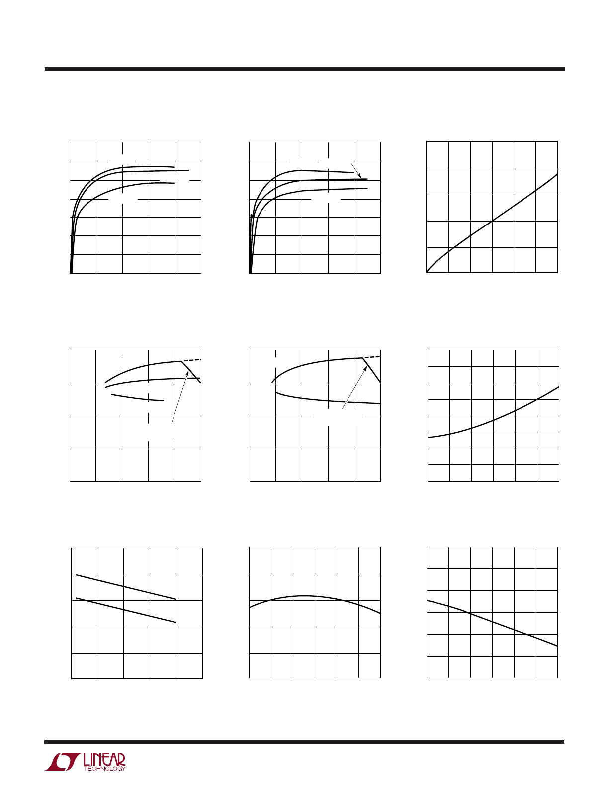
TYPICAL PERFOR A CE CHARACTERISTICS
LT1616
Efficiency, V
100
90
80
70
60
EFFICIENCY (%)
50
40
30
0
VIN = 8V
VIN = 24V
100 200 500
LOAD CURRENT (mA)
Maximum Load Current
at V
= 5V BOOST Pin Current
OUT
500
L = 15µH
400
300
LOAD CURRENT (mA)
200
100
5
0
INPUT VOLTAGE (V)
OUT
10
= 5V
L = 6.8µH
300 400
L = 10µH
OUTPUT LIMITED
BY DISSIPATION
15
VIN = 12V
20
1616 G01
1616 G04
Efficiency, V
100
90
80
70
60
EFFICIENCY (%)
50
40
30
0
100 200 500
= 3.3V Switch Voltage Drop
OUT
VIN = 5V
LOAD CURRENT (mA)
VIN = 12V
VIN = 20V
300 400
1616 G02
500
400
300
200
SWITCH VOLTAGE (mV)
100
0
0
200 400
SWITCH CURRENT (mA)
600
1616 G03
Maximum Load Current
at V
= 3.3V
OUT
500
L = 10µH
400
300
LOAD CURRENT (mA)
200
100
25
0
L = 4.7µH
5
10
INPUT VOLTAGE (V)
OUTPUT LIMITED
BY DISSIPATION
15
20
25
1616 G05
16
14
12
10
8
6
4
BOOST PIN CURRENT (mA)
2
0
0
200 400
SWITCH CURRENT (mA)
600
1616 G06
Switch Current Limit
1000
800
600
400
200
SWITCH CURRENT LIMIT (mA)
0
20
0
TYPICAL
40
DUTY CYCLE (%)
MINIMUM
60
Feedback Pin Voltage
1.27
1.26
1.25
1.24
FEEDBACK PIN VOLTAGE (V)
1.23
1.22
80
100
1616 G07
–50
02550
–25
TEMPERATURE (°C)
75 100
1616 G08
Undervoltage Lockout
3.7
3.6
3.5
3.4
3.3
UNDERVOLTAGE LOCKOUT (V)
3.2
3.1
–50
02550
–25
TEMPERATURE (°C)
75 100
1616 G11
3
Page 4
LT1616
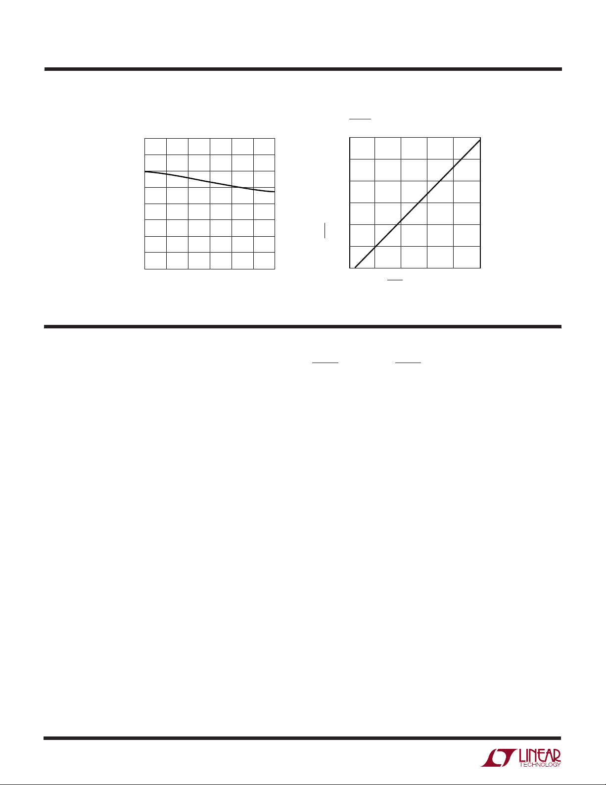
SHDN PIN VOLTAGE
0
0
SHDN PIN CURRENT (µA)
20
40
60
80
100
120
5101520
1616 G10
25
UW
TYPICAL PERFOR A CE CHARACTERISTICS
Oscillator Frequency
2.00
1.75
1.50
1.25
1.00
0.75
0.50
SWITCHING FREQUENCY (MHz)
0.25
0
U
–25 0 50
–50
25
TEMPERATURE (°C)
UU
100
75
1616 G09
PI FU CTIO S
BOOST (Pin 1): The BOOST pin is used to provide a drive
voltage, higher than the input voltage, to the internal
bipolar NPN power switch.
GND (Pin 2): Tie the GND pin to a local ground plane below
the LT1616 and the circuit components. Return the feedback divider to this pin.
FB (Pin 3): The LT1616 regulates its feedback pin to 1.25V.
Connect the feedback resistor divider tap to this pin. Set
the output voltage according to V
A good value for R2 is 10k.
= 1.25V (1 + R1/R2).
OUT
SHDN Pin Current
SHDN (Pin 4): The SHDN pin is used to put the LT1616 in
shutdown mode. Tie to ground to shut down the LT1616.
Tie to 2V or more for normal operation. If the shutdown
feature is not used, tie this pin to the VIN pin.
VIN (Pin 5): The VIN pin supplies current to the LT1616’s
internal regulator and to the internal power switch. This pin
must be locally bypassed.
SW (Pin 6): The SW pin is the output of the internal power
switch. Connect this pin to the inductor, catch diode and
boost capacitor.
4
Page 5
BLOCK DIAGRA
5
V
IN
INT REG
4
SHDN
AND
UVLO
W
LT1616
BOOST
1
SLOPE
COMP
OSC
FREQUENCY
FOLDBACK
Σ
2
GND
R
S
V
C
g
m
U
OPERATIO
The LT1616 is a constant frequency, current mode Buck
regulator. The 1.4MHz oscillator enables an RS flip-flop,
turning on the internal 600mA power switch Q1. An amplifier and comparator monitor the current flowing between
the VIN and SW pins, turning the switch off when this current
reaches a level determined by the voltage at VC. An error
amplifier measures the output voltage through an external
resistor divider tied to the FB pin. This amplifier servos the
switch current to regulate the FB pin voltage to 1.25V. An
active clamp on the VC node provides current limit.
An internal regulator provides power to the control circuitry. This regulator includes an undervoltage lockout to
prevent switching when VIN is less than ~3.5V. The
(Refer to Block Diagram)
Q
Q
1.25V
3
1616BD
FB
DRIVER
Q1
SW
6
SHDN pin is used to place the LT1616 in shutdown,
disconnecting the output and reducing the input current
to less than 1µA.
The switch driver operates from either the input or from
the BOOST pin. An external capacitor and diode are used
to generate a voltage at the BOOST pin that is higher than
the input supply. This allows the driver to fully saturate the
internal bipolar NPN power switch for efficient operation.
The oscillator reduces the LT1616’s operating frequency
when the voltage at the FB pin is low. This frequency
foldback helps to control the output current during startup and overload.
5
Page 6

LT1616
WUUU
APPLICATIO S I FOR ATIO
The LT1616 efficiently converts power from an input voltage source to a lower output voltage using an inductor for
energy storage. The LT1616 uses its internal power switch
and an external catch diode (D1 of the application circuit
on the first page of this data sheet) to produce a pulsewidth modulated square wave. Inductor L1 and output
capacitor C2 filter this square wave to produce a DC output
voltage. An error amplifier regulates the output by comparing the output (divided by the feedback resistor string
R1 and R2) to an internal reference. The LT1616 uses
current mode control; instead of directly modulating the
pulse width, the error amplifier controls the peak current
in the switch and inductor. Current mode control has several advantages, including simplified loop compensation
and cycle-by-cycle current limiting.
Figure 1 shows several waveforms of the application circuit on the front page of this data sheet. The circuit is
converting a 12V input to 3.3V at 300mA. The first trace is
the voltage at the SW pin. When the internal switch is on,
the SW pin voltage is near the 12V input. This applies a
voltage across inductor L1, and the current in the switch
(second trace) and the inductor (third trace) increases.
When the switch turns off, the switch current immediately
drops to zero and the inductor current flows through the
catch diode D1, which clamps the switch node 0.4V below
ground. The voltage across the inductor in this state has
the opposite sense and is equal to the output voltage plus
the catch diode drop, so the inductor current begins to
decrease. The fourth trace shows the output voltage ripple.
At light loads, the inductor current may reach zero on each
pulse. The diode will turn off, and the switch voltage will
ring, as shown in Figure 2. This is discontinuous mode operation, and is normal behavior for the switching regulator. The LT1616 will also skip pulses when the load is light.
V
SW
5V/DIV
I
L1
0.2A/DIV
V
SW
5V/DIV
I
SW
0.2A/DIV
200ns/DIV
I
L1
0.2A/DIV
V
OUT
5mV/DIV
200ns/DIV
Figure 1. Operating Waveforms of the LT1616
Converting 12V to 3.3V at 300mA
1616 F01a
1616 F01b
VIN = 12V 500ns/DIV
= 5V
V
OUT
I
= 18mA
OUT
Figure 2. Discontinuous Mode Operation
1616 F02
If the output is shorted to ground, the output voltage will
collapse and there will be very little voltage to reset the
current in the inductor. The LT1616 can sense this condition at its FB pin. In order to control the current, the LT1616
reduces its operating frequency, allowing more time for
the catch diode to reset the inductor current.
The input and output voltages determine the duty cycle of
the switch. The inductor value combined with these voltages determines the ripple current in the inductor. Along
with the switch current limit, the inductor ripple current
determines the maximum load current that the circuit can
supply. At minimum, the input and output capacitors are
required for stable operation. Specific values are chosen
based on allowable ripple and desired transient performance. The rest of the applications information is mainly
concerned with choosing these and the other components
in an LT1616 application.
6
Page 7

WUUU
APPLICATIO S I FOR ATIO
LT1616
Inductor Selection and Maximum Output Current
The duty cycle of the internal switch is:
DC = (V
where VD is the forward voltage drop of the catch diode
(D1) and VSW is the voltage drop of the internal switch.
Usually one is interested in DC at full load current, so you
can use VD = VSW = 0.4V. Note that the LT1616 has a
maximum guaranteed duty cycle of 0.8. This will limit the
minimum input voltage for a particular output voltage.
When the switch is off, the inductor sees the output
voltage plus the catch diode drop. This gives the peak-topeak ripple current in the inductor:
∆IL = (1 – DC)(V
where f is the switching frequency of the LT1616 and L is
the value of the inductor. The average inductor current is
equal to the output current, so the peak inductor current
will be the output current plus one half of the ripple
current:
I
= I
LPK
To maintain output regulation, this peak current must be
less than the LT1616’s switch current limit I
least 630mA at low duty cycles, decreasing to 430mA at
80% duty cycle. The maximum output current is a function
of the chosen inductor value:
+ VD)/(VIN – VSW + VD)
OUT
+ VD)/(L • f)
OUT
+ ∆IL/2.
OUT
LIM
. I
LIM
is at
If your application calls for output current less than
400mA, you may be able to relax the value of the inductor
and operate with higher ripple current. This may allow you
to pick a physically smaller inductor or one with a lower DC
resistance. Be aware that these equations assume continuous inductor current. If the inductor value is low or the
load current is light, then the inductor current may become
discontinuous. This occurs when ∆IL = 2I
of discontinuous mode operation, see Linear Technology
Application Note AN44. Also, high duty cycle operation
may require slightly higher inductor values to avoid subharmonic oscillations. See AN19.
The maximum load current as a function of input voltage
is plotted in the Typical Performance Characteristics section of this data sheet. Maximum load current for 3.3V and
5V outputs is shown for several values of L. At the highest
input voltages, the load current is limited by power dissipation in the LT1616.
Choose an inductor that is intended for power applications. Table 1 lists several manufacturers and inductor
series. The saturation current of the inductor should be
above 0.5A. The RMS current rating should be equal to or
greater than output current. For indefinite operation into a
short circuit, the RMS current rating should be greater
than 0.7A. The DC resistance should be less than 0.5Ω in
order maintain circuit efficiency.
. For details
OUT
I
OUT(MAX)
If the inductor value is chosen so that the ripple current is
small, then the available output current will be near the
switch current limit. A good approach is to choose the
inductor so that the peak-to-peak inductor ripple is equal
to one third of the switch current limit. This leads to:
L = 3(1 – DC)(V
and
I
OUT(MAX)
These expressions depend on duty cycle and therefore on
input voltage. Pick a nominal input voltage to calculate L,
then check the maximum available output current at the
minimum and maximum input voltages.
= I
– ∆IL/2.
LIM
OUT
= (5/6)I
+ VD)/(I
.
LIM
LIM •
f)
Capacitor Selection
A Buck regulator draws from its input a square wave of
current with peak-to-peak amplitude as high as the switch
current limit. The input capacitor (C1) must supply the AC
component of this current. An RMS current rating of
250mA is adequate for LT1616 circuits. The input capacitor must bypass the LT1616 internal control circuitry and
any other circuitry that operates from the input source. A
1µ F ceramic capacitor will satisfy both of these requirements. If the impedance of the input source is high (due to
long wires or filter components), additional bulk input
capacitance may be required. In high duty cycle applications (5VIN to 3.3V
capacitor to 2.2µ F. It may be possible to achieve lower cost
by using an electrolytic capacitor (tantalum or aluminum)
, for example), increase the input
OUT
7
Page 8

LT1616
WUUU
APPLICATIO S I FOR ATIO
Table 1. Inductor Vendors
Vendor Phone URL Part Series Comments
Murata (404) 426-1300 www.murata.com LQH3C Small, Low Cost, 2mm Height
Sumida (847) 956-0666 www.sumida.com CR43
Coilcraft (847) 639-6400 www.coilcraft.com DO1607C
Coiltronics (407) 241-7876 www.coiltronics.com CTXxx-1 1:1 Coupled Toroid
Toko www.tokoam.com 3DF
Table 2. Capacitor Vendors
Vendor Phone URL Part Series Comments
Taiyo-Yuden (408) 573-4150 www.t-yuden.com Ceramic Caps X5R Dielectric
AVX (803) 448-9411 www.avxcorp.com Ceramic Caps
Murata (404) 436-1300 www.murata.com Ceramic Caps
CLS62 1:1 Coupled
CLQ61 1.5mm Height
DO1608C
DT1608C
TP1 1.8mm Height
D52LC
Tantalum Caps
in combination with a 0.1µ F ceramic capacitor. However,
input voltage ripple will be higher, and you may want to
include an additional 0.1µ F ceramic a short distance away
from the LT1616 circuit in order to filter the high frequency
ripple. The input capacitor should be rated for the maximum input voltage.
The output capacitor has two essential functions. Along
with the inductor, it filters the square wave generated by
the LT1616 to produce the DC output. In this role it
determines the output ripple. The second function is to
store energy in order to satisfy transient loads and stabilize the LT1616’s control loop.
In most switching regulators the output ripple is determined by the equivalent series resistance (ESR) of the
output capacitor. Because the LT1616’s control loop doesn’t
depend on the output capacitor’s ESR for stable operation,
you are free to use ceramic capacitors to achieve very low
output ripple and small circuit size. You can estimate
output ripple with the following equations:
V
= ∆IL • ESR for electrolytic capacitors (tantalum
RIPPLE
and aluminum)
V
= ∆IL/(2π • f • C
RIPPLE
) for ceramic capacitors
OUT
Another constraint on the output capacitor is that it must
have greater energy storage than the inductor; if the stored
energy in the inductor is transferred to the output, you
would like the resulting voltage step to be small compared
to the regulation voltage. For a 5% overshoot, this requirement becomes
C
OUT
> 10 • L(I
LIM/VOUT
2
)
Finally, there must be enough capacitance for good transient performance. The last equation gives a good starting
point. Alternatively, you can start with one of the designs
in this data sheet and experiment to get the desired
performance. Figure 3 illustrates some of the trade-off
between different output capacitors. Figure 4 shows the
test circuit. The lowest trace shows total output current,
which jumps from 100mA to 250mA. The other traces
show the output voltage ripple and transient response
with different output capacitors. The capacitor value, size
and type are listed. Note that the time scale at 50µs per
divison is much larger than the switching period, so you
can’t see the output ripple at the switching frequency. The
output ripple appears as vertical broadening of the trace.
The first trace (C
= 4.7µF) has peak-to-peak output
OUT
ripple of ~ 6mV, while the third trace shows peak-to-peak
ripple of ~15mV.
8
Page 9

WUUU
APPLICATIO S I FOR ATIO
LT1616
C
= 4.7µF CERAMIC, CASE SIZE 0805
OUT
C
= 10µF CERAMIC, CASE SIZE 1206
OUT
C
= 47µF, ESR ≅ 0.080Ω (SANYO POSCAP 6TPA47M)
OUT
C CASE
C
= 100µF, ESR ≅ 0.150Ω (TANTALUM AVX
OUT
TPSC107M006R0150) C CASE
V
10V
5
IN
VINBOOST
LT1616
4
SHDN SW
GND FB
23
1
6
10µH
V
OUT
3.3V
22Ω
33Ω
C
OUT
1616 F04
Figure 4. Circuit Used for Transient Load Test Shown in Figure 3
Regardless of which capacitor or combination of capacitors you choose, you should do transient load tests to
evaluate the circuit’s stability. Avoid capacitors or combinations that result in a ringing response. Problems may
occur if the output capacitance is very low or if a high value
inductor is used in combination with a large value, low
ESR capacitor.
The high performance (low ESR), small size and robustness of ceramic capacitors make them the preferred type
for LT1616 applications. However, all ceramic capacitors
are not the same. Many of the higher value capacitors use
poor dielectrics with high temperature and voltage
coefficients. In particular, Y5V types should be regarded
with suspicion. Stick with X7R and X5R types. Don’t be
afraid to run them at their rated voltage. Table 2 lists
several capacitor manufacturers.
Catch Diode
V
OUT
20mV/DIV
I
LOAD
100mA/DIV
0
C
= 100µF TANTALUM AND 2.2µF CERAMIC
OUT
Figure 3. Transient Load Response of the LT1616
A 0.5A Schottky diode is recommended for the catch diode
D1. The ON Semiconductor MBR0530 is a good choice; it
is rated for 0.5A forward current and a maximum reverse
voltage of 30V. For circuits with VIN less than 20V, the
MBR0520L can be used. Other suitable diodes are the
Zetex ZHCS500TR and ZHCS750TR, and various versions
of the 1N5818.
9
Page 10

LT1616
LOAD CURRENT (mA)
1
INPUT VOLTAGE (V)
6
7
10 100 500
1616 F06a
5
4
3
BOOST DIODE
TIED TO OUTPUT
V
OUT
= 3.3V
D
BOOST
= BAT54
BOOST DIODE
TIED TO INPUT
V TO START
V TO RUN
LOAD CURRENT (mA)
1
INPUT VOLTAGE (V)
7
8
9
10 100 500
1616 F06b
6
5
4
BOOST DIODE
TIED TO OUTPUT
V
OUT
= 5V
D
BOOST
= BAT54
V TO START
V TO RUN
BOOST DIODE
TIED TO INPUT
WUUU
APPLICATIO S I FOR ATIO
BOOST Pin Considerations
Capacitor C3 and diode D2 are used to generate a boost
voltage that is higher than the input voltage. In most cases
a 0.01µ F capacitor and fast switching diode (such as the
1N4148 or 1N914) will work well. Figure 5 shows two
ways to arrange the boost circuit. The BOOST pin must be
more than 2.5V above the SW pin for best efficiency. For
outputs of 3.3V and above, the standard circuit (Figure 5a)
is best. For outputs between 2.8V and 3.3V, use a 0.033µ F
capacitor and a small Schottky diode (such as the
BAT-54). For lower output voltages the boost diode can be
tied to the input (Figure 5b). The circuit in Figure 5a is more
efficient because the BOOST pin current comes from a
lower voltage source. You must also be sure that the
maximum voltage rating of the BOOST pin is not exceeded.
The minimum operating voltage of an LT1616 application
is limited by the undervoltage lockout (<3.6V) and by the
maximum duty cycle as outlined above. For proper startup, the minimum input voltage is also limited by the boost
circuit. If the input voltage is ramped slowly, or the LT1616
is turned on with its SHDN pin when the output is already
in regulation, then the boost capacitor may not be fully
charged. Because the boost capacitor is charged with the
energy stored in the inductor, the circuit will rely on some
minimum load current to get the boost circuit running
properly. This minimum load will depend on input and
output voltages, and on the arrangement of the boost
circuit. The minimum load generally goes to zero once the
circuit has started. Figure 6 shows a plot of minimum load
to start and to run as a function of input voltage. In many
cases the discharged output capacitor will present a load
to the switcher which will allow it to start. The plots show
the worst-case situation where VIN is ramping very slowly.
Use a Schottky diode (such as the BAT-54) for the lowest
start-up voltage.
Minimum Input Voltage V
OUT
= 3.3V
10
D2
C3
V
OUT
Minimum Input Voltage V
1616 F05a
C3
V
OUT
1616 F05b
OUT
= 5V
V
IN
V
BOOST
MAX V
V
IN
V
BOOST
MAX V
V
IN
– VSW ≅ V
BOOST
D2
V
IN
– VSW ≅ V
BOOST
BOOST
LT1616
GND
≅ VIN + V
BOOST
LT1616
GND
≅ 2V
SW
OUT
OUT
(5a)
SW
IN
IN
(5b)
Figure 5. Two Circuits for Generating the Boost Voltage Figure 6. The Minimum Input Voltage Depends
on Output Voltage, Load Current and Boost Circuit
Page 11

WUUU
APPLICATIO S I FOR ATIO
LT1616
Shorted Input Protection
If the inductor is chosen so that it won’t saturate excessively, an LT1616 buck regulator will tolerate a shorted
output. There is another situation to consider in systems
where the output will be held high when the input to the
LT1616 is absent. This may occur in battery charging
applications or in battery backup systems where a battery
or some other supply is diode OR-ed with the LT1616’s
output. If the VIN pin is allowed to float and the SHDN pin
is held high (either by a logic signal or because it is tied to
VIN), then the LT1616’s internal circuitry will pull its
quiescent current through its SW pin. This is fine if your
system can tolerate a few mA in this state. If you ground
D4
100k
100k
5
V
IN
LT1616
4
SHDN SW
GND FB
23
V
IN
BOOST
1
6
the SHDN pin, the SW pin current will drop to essentially
zero. However, if the VIN pin is grounded while the output
is held high, then parasitic diodes inside the LT1616 can
pull large currents from the output through the SW pin and
the VIN pin. Figure 7 shows a circuit that will run only when
the input voltage is present and that protects against a
shorted or reversed input.
PCB Layout
For proper operation and minimum EMI, care must be
taken during printed circuit board layout. Figure 8 shows
the high current paths in the buck regulator circuit. Note
that large, switched currents flow in the power switch, the
V
OUT
BACKUP
D4: MBR0530
1616 F07
Figure 7. Diode D4 Prevents a Shorted Input from Discharging a
Backup Battery Tied to the Output; It Also Protects the Circuit from a
Reversed Input. The LT1616 Runs Only When the Input is Present
V
SW
IN
GND
(a)
I
C1
V
SW
IN
C1 D1 C2
GND
(c)
V
SW
IN
GND
(b)
V
L1
SW
1616 F08
Figure 8. Subtracting the Current When the Switch is On (a) from the Current When the Switch is Off (b) Reveals the Path of the High
Frequency Switching Current (c). Keep This Loop Small. The Voltage on the SW and BOOST Nodes Will Also be Switched; Keep These
Nodes as Small as Possible. Finally, Make Sure the Circuit is Shielded with a Local Ground Plane
11
Page 12

LT1616
WUUU
APPLICATIO S I FOR ATIO
catch diode (D1) and the input capacitor (C1). The loop
formed by these components should be as small as
possible. Furthermore, the system ground should be tied
to the regulator ground in only one place; this prevents the
switched current from injecting noise into the system
ground. These components, along with the inductor and
output capacitor, should be placed on the same side of the
circuit board, and their connections should be made on
that layer. Place a local, unbroken ground plane below
these components, and tie this ground plane to system
ground at one location, ideally at the ground terminal of the
output capacitor C2. Additionally, the SW and BOOST
nodes should be kept as small as possible. Finally, keep
the FB node as small as possible so that the ground pin and
ground traces will shield it from the SW and BOOST nodes.
Figure 9 shows component placement with trace, ground
plane and via locations. Include two vias near the GND pin
of the LT1616 to help remove heat from the LT1616 to the
ground plane.
Outputs Greater than 6V
For outputs greater than 6V, connect a diode (such as a
1N4148) from the SW pin to VIN to prevent the SW pin
from ringing above VIN during discontinuous mode operation. The 12V output circuit below shows the location of
this diode. Also note that for outputs above 10V, the input
voltage range will be limited by the maximum rating of the
BOOST pin. The 12V circuit shows how to overcome this
limitation using an additional Zener diode.
Other Linear Technology Publications
Application notes AN19, AN35 and AN44 contain more
detailed descriptions and design information for Buck
regulators and other switching regulators. The LT1376
data sheet has a more extensive discussion of output
ripple, loop compensation and stability testing. Design
Note DN100 shows how to generate a bipolar output
supply using a Buck regulator.
12
SHUTDOWN
V
IN
VIAS TO LOCAL GROUND PLANE
OUTLINE OF LOCAL GROUND PLANE
Figure 9. A Good PCB Layout Ensures Proper, Low EMI Operation
1616 F09
V
OUT
SYSTEM
GROUND
Page 13

TYPICAL APPLICATIO S
V
16V TO 25V
OFF ON
U
12V Output
D4
IN
5
V
4
SHDN SW
C1
1µF
25V
C1: TAIYO-YUDEN TMK316BJ105ML
C2: TAIYO-YUDEN EMK316BJ225ML
D1: ON SEMICONDUCTOR MBR0530
D2, D4: 1N4148
D3: CMPZ5234B 6.2V ZENER.
D3 LIMITS BOOST PIN VOLTAGE TO V
L1: COILCRAFT DO1608C-333
BOOST
IN
LT1616
GND FB
23
R2
10k
1
6
R1
86.6k
C3
0.01µF
D1
IN
D2
+ 6V
L1
33µH
2.2µF
16V
LT1616
D3
V
OUT
12V
300mA
C2
GND
1616 TA03
V
3.6V TO 12V
OFF ON
1.8V Output
D2
IN
5
V
4
SHDN SW
C1
1µF
16V
C1: TAIYO-YUDEN EMK212BJ105MG
C2: TAIYO-YUDEN JMK316BJ106ML
D1: ON SEMICONDUCTOR MBR0520L
D2: 1N4148 OR EQUIVALENT
L1: MURATA LQH3C4R7M24
BOOST
IN
LT1616
GND FB
23
R2
20k
1
6
R1
8.87k
C3
0.01µF
D1
L1
4.7µH
10µF
6.3V
V
OUT
400mA
C2
GND
1616 TA04
13
Page 14

LT1616
TYPICAL APPLICATIO S
U
2.5V Output
D2
V
3.6V TO 16V
OFF ON
V
IN
7V TO 25V
OFF ON
IN
5
V
4
SHDN SW
C1
1µF
16V
C1: TAIYO-YUDEN EMK212BJ105MG
C2: TAIYO-YUDEN JMK212BJ475MG
D1: ON SEMICONDUCTOR MBR0520
D2: 1N4148
L1: MURATA LQH3C4R7M24
BOOST
IN
LT1616
GND FB
23
5V Output
5
V
4
SHDN SW
C1
1µF
25V
C1: TAIYO-YUDEN TMK316BJ105ML
C2: TAIYO-YUDEN JMK316BJ106MG
D1: ON SEMICONDUCTOR MBR0530
D2: 1N4148
L1: TOKO A914BYW-150M
BOOST
IN
LT1616
GND FB
23
R2
10k
R2
10k
1
6
1
6
R1
30.1k
R1
10k
C3
0.01µF
C3
0.01µF
D1
L1
4.7µH
D1
C2
4.7µF
6.3V
D2
L1
15µH
1616 TA05
V
OUT
2.5V
350mA
GND
V
OUT
5V
300mA: V
400mA: V
C2
10µF
6.3V
1616 TA07
= 7V TO 25V
IN
= 8V TO 25V
IN
14
Page 15

PACKAGE DESCRIPTION
LT1616
U
Dimensions in inches (millimeters) unless otherwise noted.
S6 Package
6-Lead Plastic SOT-23
(LTC DWG # 05-08-1634)
2.80 – 3.00
(0.110 – 0.118)
(NOTE 3)
1.90
2.6 – 3.0
(0.110 – 0.118)
1.50 – 1.75
(0.059 – 0.069)
0.35 – 0.55
(0.014 – 0.022)
NOTE:
1. DIMENSIONS ARE IN MILLIMETERS
2. DIMENSIONS ARE INCLUSIVE OF PLATING
3. DIMENSIONS ARE EXCLUSIVE OF MOLD FLASH AND METAL BURR
4. MOLD FLASH SHALL NOT EXCEED 0.254mm
5. PACKAGE EIAJ REFERENCE IS SC-74A (EIAJ)
0.09 – 0.20
(0.004 – 0.008)
(NOTE 2)
(0.074)
REF
0.00 – 0.15
(0.00 – 0.006)
0.35 – 0.50
(0.014 – 0.020)
SIX PLACES (NOTE 2)
0.95
(0.037)
REF
0.90 – 1.45
(0.035 – 0.057)
0.90 – 1.30
(0.035 – 0.051)
S6 SOT-23 0898
Information furnished by Linear Technology Corporation is believed to be accurate and reliable.
However, no responsibility is assumed for its use. Linear Technology Corporation makes no representation that the interconnection of its circuits as described herein will not infringe on existing patent rights.
15
Page 16

LT1616
TYPICAL APPLICATION
U
Bipolar Output DC/DC Converter
V
IN
7.5V TO 25V
OFF ON
C1: TAIYO-YUDEN TMK316BJ105ML
C2, C4: TAIYO-YUDEN JMK316BJ106ML
C5: TAIYO-TUDEN JMK107BJ105MA
D1, D3: ON SEMICONDUCTOR MBR0530
D2: 1N4148
L1: 22µH 1:1 SUMIDA CLS62-220 OR
COILTRONICS CTX20-1
–5V LOAD SHOULD BE LESS THAN
1/2 5V LOAD, SEE DESIGN NOTE 100
5
V
IN
4
SHDN SW
GND FB
C1
1µF
25V
1
BOOST
LT1616
23
6
R1
30.1k
R2
10k
C5
1µF
6.3V
C3
0.01µF
D1
•
D3
D2
•
L1B
22µH
L1A
22µH
10µF
6.3V
C2
10µF
6.3V
C4
1616 TA06
5V
200mA
GND
–5V
100mA
RELATED PARTS
PART NUMBER DESCRIPTION COMMENTS
LTC®1474/LTC1475 0.5A Micropower Step-Down Regulator 10µA IQ, 100% Duty Cycle, 8-Lead MSOP Package
LT1676/LT1776 Wide Input Range Step-Down Switching Regulator 60V Input, 0.7A Internal Switch
LTC1701 0.5A Micropower Step-Down in SOT-23 100% Duty Cycle, High Efficiency: Up to 94%
LT1763 500mA, Low Noise, LDO Micropower Regulator 30µA IQ, 20µV
LT1767 1.5A, 1.4MHz Step-Down DC/DC Converter Higher Current, 8-Lead MSOP Package
LTC1772 Constant Frequency Step-Down Controller in SOT-23 Higher Current, High Efficiency: Up to 94%
LTC1779 0.25A Micropower Step-Down in SOT-23 Lower Current, 100% Duty Cycle
LTC1877 0.6A Synchronous Step-Down Regulator High Efficiency, No Diode Required, 8-Lead MSOP
LT1962 300mA, Low Noise, LDO Micropower Regulator 30µA IQ, 20µV
Noise
RMS
Noise, 8-Lead MSOP Package
RMS
16
Linear T echnology Corporation
1630 McCarthy Blvd., Milpitas, CA 95035-7417
(408) 432-1900 ● FAX: (408) 434-0507
●
www.linear-tech.com
sn1616 1616fs LT/TP 0201 4K • PRINTED IN USA
LINE AR TECHNOLOGY CO RP O R ATION 2000
 Loading...