

FEATURES
LT1614
Inverting 600kHz
Switching Regulator
U
DESCRIPTIO
■
Better Regulation Than a Charge Pump
■
0.1Ω Effective Output Impedance
■
–5V at 200mA from a 5V Input
■
600kHz Fixed Frequency Operation
■
Operates with VIN as Low as 1V
■
1mA Quiescent Current
■
Low Shutdown Current: 10µA
■
Low-Battery Detector
■
Low V
Switch: 295mV at 500mA
CESAT
U
APPLICATIO S
■
MR Head Bias
■
LCD Bias
■
GaAs FET Bias
■
Positive-to-Negative Conversion
U
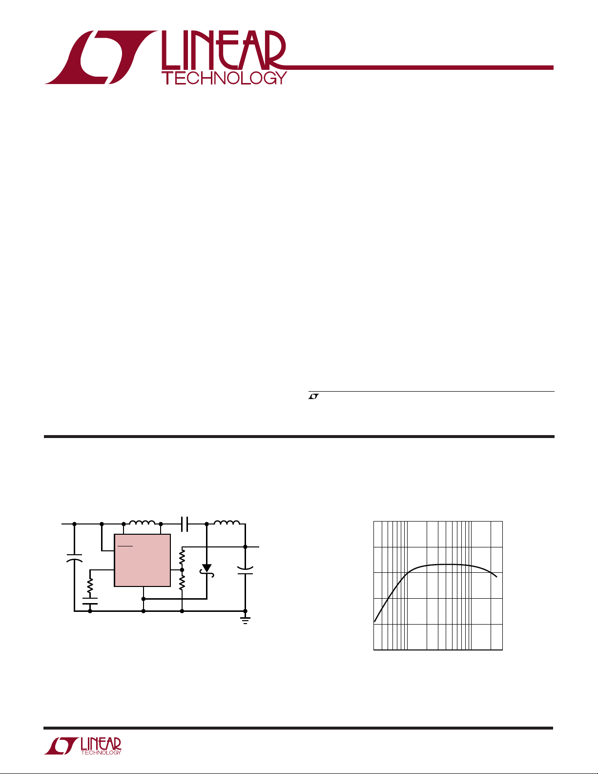
TYPICAL APPLICATIO
The LT®1614 is a fixed frequency, inverting mode switching reglator that operates from an input voltage as low as
1V. Utilizing a low noise topology, the LT1614 can generate a negative output down to – 24V from a 1V to 5V input.
Fixed frequency switching ensures a clean output free
from low frequency noise. The device contains a lowbattery detector with a 200mV reference and shuts down
to less than 10µA. No load quiescent current of the LT1614
is 1mA and the internal NPN power switch handles a
500mA current with a voltage drop of just 295mV.
High frequency switching enables the use of small inductors and capacitors. Ceramic capacitors can be used in
many applications, eliminating the need for bulky tantalum types.
The LT1614 is available in 8-lead MSOP or SO packages.
, LTC and LT are registered trademarks of Linear Technology Corporation.
V
IN
5V
+
C1
33µF
C1, C2: AVX TAJB336M010
C3: TAIYO YUDEN EMK316BJ105MF
D1: MBR0520
L1, L2: MURATA LQH3C220
SHDN
V
100k
1nF
Figure 1. 5V to –5V/200mA Converter
SW
NFB
C3
1µF
69.8k
24.9k
D1
L2
22µH
C2
+
33µF
1614 TA01
V
OUT
–5V
200mA
5V to –5V Converter Efficiency
90
80
70
60
EFFICIENCY (%)
50
40
31030
LOAD CURRENT (mA)
100 300
1614 TA02
L1
22µH
V
IN
LT1614
C
GND
1

LT1614
1
2
3
4
8
7
6
5
TOP VIEW
LBO
LBI
V
IN
SW
NFB
V
C
SHDN
GND
S8 PACKAGE
8-LEAD PLASTIC SO
A
W
O
LUTEXI TIS
S
A
WUW
U
ARB
G
VIN, SHDN, LBO Voltage ......................................... 12V
SW Voltage ............................................... –0.4V to 30V
NFB Voltage ............................................................ –3V
VC Voltage ................................................................ 2V
LBI Voltage ............................................ 0V ≤ V
LBI
≤ 1V
Current into FB Pin .............................................. ±1mA
Junction Temperature...........................................125°C
WU
/
PACKAGE
NFB
1
V
2
C
3
SHDN
4
GND
8-LEAD PLASTIC MSOP
T
JMAX
O
RDER I FOR ATIO
TOP VIEW
8
LBO
7
LBI
6
V
5
SW
MS8 PACKAGE
= 125°C, θJA = 160°C/W
ORDER PART
NUMBER
LT1614CMS8
LT1614IMS8
IN
MS8 PART MARKING
LTID
LTJB
(Note 1)
Operating Temperature Range
LT1614C................................................. 0°C to 70°C
LT1614I ............................................. – 40°C to 85°C
Extended Commercial
Temperature Range (Note 2) .................. –40°C to 85°C
Storage Temperature Range ................ –65°C to 150°C
Lead Temperature (Soldering, 10 sec)................. 300°C
U
ORDER PART
NUMBER
LT1614CS8
LT1614IS8
S8 PART MARKING
T
= 125°C, θJA = 120°C/W
JMAX
1614
1614I
Consult factory for Military grade parts.
LECTRICAL C CHARA TERIST
E
temperature range, otherwise specifications are at TA = 25°C. Commercial Grade 0°C to 70°C. VIN = 1.5V, V
otherwise noted.
PARAMETER CONDITIONS MIN TYP MAX UNITS
Quiescent Current 12mA
Feedback Voltage ● –1.21 –1.24 –1.27 V
NFB Pin Bias Current (Note 3) V
Reference Line Regulation 1V ≤ VIN ≤ 2V 0.6 1.1 %/V
Minimum Input Voltage 0.92 1 V
Maximum Input Voltage ● 6V
Error Amp Transconductance ∆I = 5µA16µmhos
Error Amp Voltage Gain 100 V/V
Switching Frequency ● 500 600 750 kHz
Maximum Duty Cycle 73 80 %
Switch Current Limit (Note 4) 0.75 1.2 A
The ● denotes the specifications which apply over the full operating
ICS
= VIN unless
SHDN
V
= 0V 5 10 µA
SHDN
= –1.24V ● –2.5 –4.5 –7 µA
NFB
2V ≤ V
≤ 6V 0.3 0.8 %/V
IN
● 70 80 %
2

LT1614
LECTRICAL C CHARA TERIST
E
temperature range, otherwise specifications are at TA = 25°C. Commercial Grade 0°C to 70°C. VIN = 1.5V, V
otherwise noted.
PARAMETER CONDITIONS MIN TYP MAX UNITS
Switch V
Shutdown Pin Current V
LBI Threshold Voltage 190 200 210 mV
LBO Output Low I
LBO Leakage Current V
LBI Input Bias Current (Note 5) V
Low-Battery Detector Gain 1MΩ Load 1000 V/V
Switch Leakage Current VSW = 5V 0.01 3 µA
CESAT
ICS
The ● denotes the specifications which apply over the full operating
= VIN unless
SHDN
ISW = 500mA (25°C, 0°C) 295 350 mV
= 500mA (70°C) 400 mV
I
SW
= V
SHDN
IN
= 0V –5 – 10 µA
V
SHDN
● 185 215 mV
= 10µA 0.1 0.25 V
SINK
= 250mV, V
LBI
= 150mV 10 50 nA
LBI
= 5V 0.01 0.1 µA
LBO
10 20 µA
Industrial Grade –40°C to 85°C. VIN = 1.5V, V
PARAMETER CONDITIONS MIN TYP MAX UNITS
Quiescent Current 12mA
Feedback Voltage ● –1.21 –1.24 –1.27 V
NFB Pin Bias Current (Note 3) V
Reference Line Regulation 1V ≤ VIN ≤ 2V 0.6 1.1 %/V
Minimum Input Voltage – 40°C 1.1 1.25 V
Maximum Input Voltage ● 6V
Error Amp Transconductance ∆I = 5µA16µmhos
Error Amp Voltage Gain 100 V/V
Switching Frequency ● 500 600 750 kHz
Maximum Duty Cycle ● 70 80 %
Switch Current Limit (Note 4) 0.75 1.2 A
Switch V
Shutdown Pin Current V
LBI Threshold Voltage ● 180 200 220 mV
LBO Output Low I
LBO Leakage Current V
LBI Input Bias Current (Note 5) V
Low-Battery Detector Gain 1MΩ Load 1000 V/V
Switch Leakage Current VSW = 5V 0.01 3 µA
Note 1: Absolute Maximum Ratings are those values beyond which the life
of a device may be impaired.
Note 2: The LT1614C is guaranteed to meet specified performance from
0°C to 70°C and is designed, characterized and expected to meet these
extended temperature limits, but is not tested at –40°C and 85°C. The
LT1614I is guaranteed to meet the extended temperature limits.
CESAT
= VIN unless otherwise noted.
SHDN
= 0V 5 10 µA
V
SHDN
= –1.24V ● –2 – 4.5 –7.5 µA
NFB
≤ 6V 0.3 0.8 %/V
2V ≤ V
IN
85°C 0.8 1.0 V
ISW = 500mA (–40°C) 250 350 mV
= 500mA (85°C) 330 400 mV
I
SW
= V
SHDN
IN
= 0V –5 – 10 µA
V
SHDN
= 10µA 0.1 0.25 V
SINK
= 250mV, V
LBI
= 150mV 5 30 nA
LBI
Note 3: Bias current flows out of NFB pin.
Note 4: Switch current limit guaranteed by design and/or correlation to
static tests. Duty cycle affects current limit due to ramp generator.
Note 5: Bias current flows out of LBI pin.
10 20 µA
= 5V 0.1 0.3 µA
LBO
3
LT1614
UW
TYPICAL PERFOR A CE CHARACTERISTICS
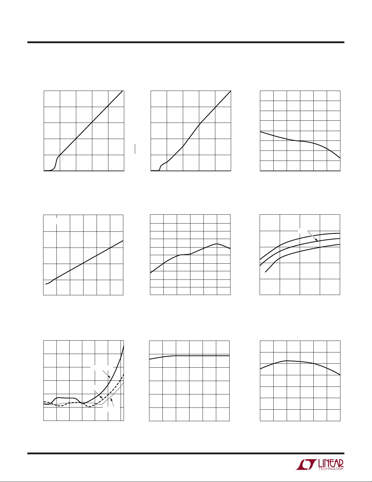
Shutdown Pin Bias Current vs
Input Voltage
10
8
6
4
QUIESCENT CURRENT (µA)
2
0
012345
INPUT VOLTAGE (V)
500
400
300
(mV)
CESAT
200
V
100
Switch V
TA = 25°C
0
0
100
vs Current
CESAT
200 300 400
SWITCH CURRENT (mA)
500 600
1614 G01
1614 G04
10
8
6
4
SHDN BIAS CURRENT (µA)
2
0
012345
INPUT VOLTAGE (V)
210
208
206
204
202
200
198
196
REFERENCE VOLTAGE (mV)
194
192
190
–50
–25
0
TEMPERATURE (°C)
25 50
LBI Bias Current vs TemperatureQuiescent Current in Shutdown
16
14
12
10
8
6
LBI BIAS CURRENT (nA)
4
2
0
1614 G02
–25 0 50
–50
TEMPERATURE (°C)
25
75
100
1614 G03
Oscillator Frequency vs
Input VoltageLBI Reference vs Temperature
900
800
700
600
FREQUENCY (kHz)
500
100
75
1614 G05
400
1
2
25°C
85°C
–40°C
3
INPUT VOLTAGE (V)
4
5
1614 G06
Quiescent Current vs
Temperature*
6
5
4
3
2
QUIESCENT CURRENT (mA)
1
0
–40–200 20406080
TEMPERATURE (°C)
*Includes diode leakage
VIN = 1.25V
VIN = 3V
4
VIN = 5V
1614 G07
NFB Pin Bias Current vs
Temperature
6
5
4
3
2
NFB PIN BIAS CURRENT (µA)
1
0
–50 0 50–25 25 75 100
TEMPERATURE (°C)
1614 G08
V
vs Temperature
NFB
–1.245
–1.240
–1.235
–1.230
(V)
NFB
V
–1.225
–1.220
–1.215
–1.210
–50 0 50–25 25 75 100
TEMPERATURE (°C)
1614 G09
UUU
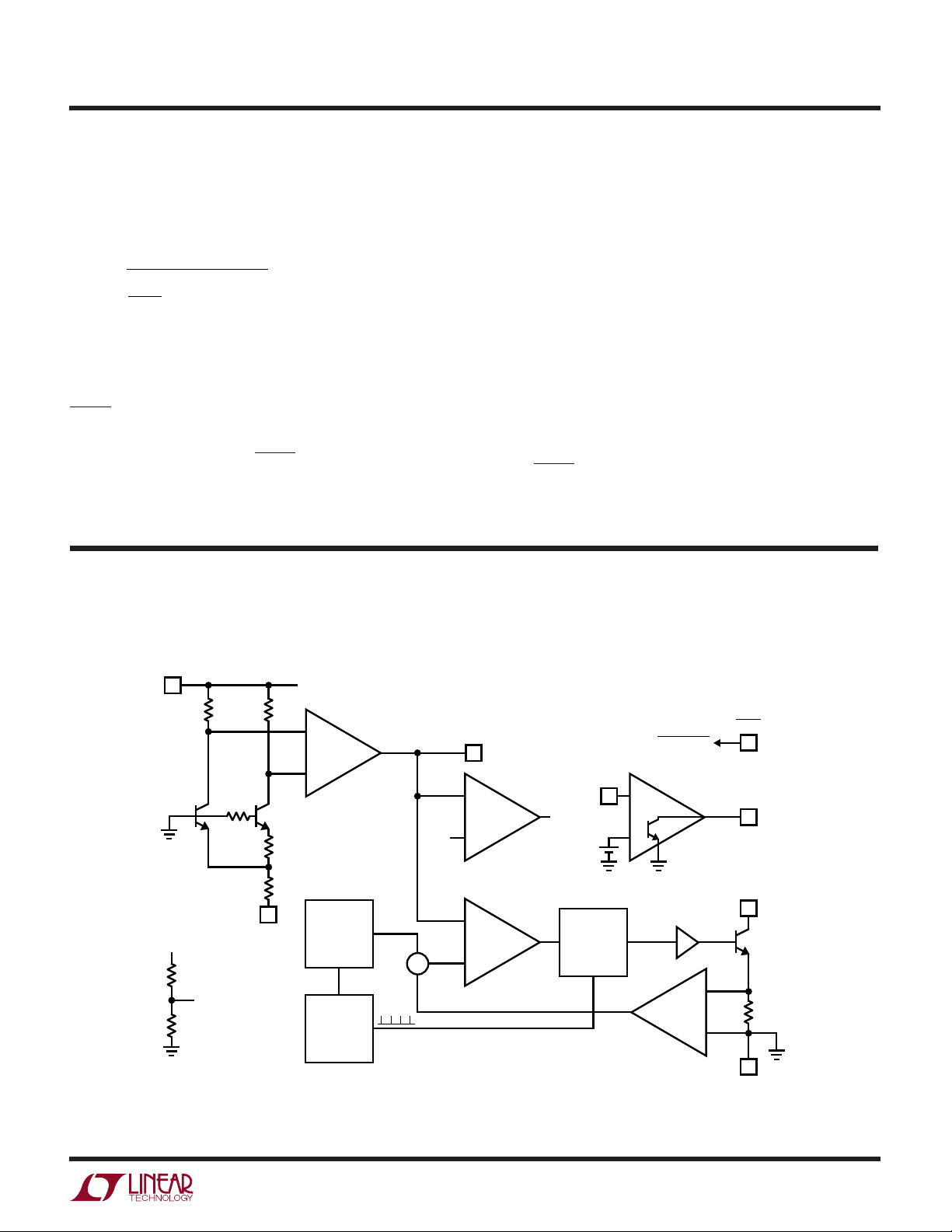
PIN FUNCTIONS
LT1614
NFB (Pin 1): Negative Feedback Pin. Reference voltage is
–1.24V. Connect resistive divider tap here. The suggested value for R2 is 24.9k. Set R1 and R2 according to:
||–.
V
.
124
R
2
OUT
+
R
1
=
124
.•
45 10
6
–
VC (Pin 2): Compensation Pin for Error Amplifier. Connect a series RC from this pin to ground. Typical values
are 100kΩ and 1nF. Minimize trace area at VC.
SHDN (Pin 3): Shutdown. Ground this pin to turn off
switcher. Must be tied to VIN (or higher voltage) to enable
switcher. Do not float the SHDN pin.
W
BLOCK DIAGRAM
GND (Pin 4): Ground. Connect directly to local ground
plane.
SW (Pin 5): Switch Pin. Minimize trace area at this pin to
keep EMI down.
VIN (Pin 6): Supply Pin. Must have 1µF ceramic bypass
capacitor right at the pin, connected directly to ground.
LBI (Pin 7): Low-Battery Detector Input. 200mV reference. Voltage on LBI must stay between ground and
700mV. Float this pin if not used.
LBO (Pin 8): Low-Battery Detector Output. Open collector, can sink 10µA. A 1MΩ pull-up is recommended. Float
this pin if not used. The low-battery detector is disabled
when SHDN is low. LBO is high-Z in this state.
V
IN
6
V
OUT
R1
(EXTERNAL)
R2
(EXTERNAL)
NFB
V
IN
NFB
1
Q2
×10
R6
40k
R3
30k
R4
140k
+
g
m
–
ERROR
AMPLIFIER
A1
RAMP
GENERATOR
600kHz
OSCILLATOR
V
C
2
LBI
+
ENABLE
BIAS
–
COMPARATOR
–
+
Σ
+
+
A2
7
200mV
FF
R
S
SHUTDOWN
+
–
A4
DRIVER
Q
A = 3
SHDN
3
LBO
8
SW
5
Q3
+
0.15Ω
–
4
1614 BD
GND
R5
40k
Q1
Figure 2. Block Diagram
5

LT1614
OPERATIO
U
The LT1614 combines a current mode, fixed frequency
PWM architecture with a –1.23V reference to directly
regulate negative outputs. Operation can be best understood by referring to the block diagram of Figure 2. Q1 and
Q2 form a bandgap reference core whose loop is closed
around the output of the converter. The driven reference
point is the lower end of resistor R4, which normally sits
at a voltage of –1.23V. As the load current changes, the
NFB pin voltage also changes slightly, driving the output
of gm amplifier A1. Switch current is regulated directly on
a cycle-to-cycle basis by A1’s output. The flip-flop is set at
the beginning of each cycle, turning on the switch. When
the summation of a signal representing switch current and
a ramp generator (introduced to avoid subharmonic oscillations at duty factors greater than 50%) exceeds the V
C
signal, comparator A2 changes stage, resetting the flipflop and turning off the switch. Output voltage decreases
(the magnitude increases) as switch current is increased.
The output, attenuated by external resistor divider R1 and
R2, appears at the NFB pin, closing the overall loop.
Frequency compensation is provided externally by a series
RC connected from the VC pin to ground. Typical values
are 100k and 1nF. Transient response can be tailored by
adjustment of these values.
As load current is decreased, the switch turns on for a
shorter period each cycle. If the load current is further
decreased, the converter will skip cycles to maintain
output voltage regulation.
C2
V
SHUTDOWN
L1
IN
+
V
C1
10Ok
1nF
IN
SHDN
V
C
LT1614
GND
1µF
SW
R1
NFB
R2
10k
D2
D1
–V
OUT
C3
+
The LT1614 can work in either of two topologies. The
simpler topology appends a capacitive level shift to a
boost converter, generating a negative output voltage,
which is directly regulated. The circuit schematic is detailed in Figure 3. Only one inductor is required, and the
two diodes can be in a single SOT-23 package. Output
noise is the same as in a boost converter, because current
is delivered to the output only during the time when the
LT1614’s internal switch is on.
If D2 is replaced by an inductor, as shown in Figure 4, a
higher performance solution results. This converter topology was developed by Professor S. Cuk of the California
Institute of Technology in the 1970s. A low ripple voltage
results with this topology due to inductor L2 in series with
the output. Abrupt changes in output capacitor current are
eliminated because the output inductor delivers current to
the output during both the off-time and the on-time of the
LT1614 switch. With proper layout and high quality output
capacitors, output ripple can be as low as 1mV
P–P
.
The operation of Cuk’s topology is shown in Figures 5
and␣ 6. During the first switching phase, the LT1614’s
switch, represented by Q1, is on. There are two current
loops in operation. The first loop begins at input capacitor
C1, flows through L1, Q1 and back to C1. The second loop
flows from output capacitor C3, through L2, C2, Q1 and
back to C3. The output current from R
L2 and C3. The voltage at node SW is V
SWX the voltage is –(VIN + |V
|). Q1 must conduct both
OUT
is supplied by
LOAD
and at node
CESAT
L1 and L2 current. C2 functions as a voltage level shifter,
with an approximately constant voltage of (VIN + |V
across it.
V
IN
L1 L2
+
V
IN
C1
10Ok
1nF
LT1614
SHDNSHUTDOWN
V
C
GND
SW
NFB
C2
1µF
D1
R1
R2
10k
OUT
C3
+
–V
|)
OUT
6
Figure 3. Direct Regulation of Negative Output
Using Boost Converter with Charge Pump
1614 F03
1614 F04
Figure 4. L2 Replaces D2 to Make Low Output Ripple
Inverting Topology. Coupled or Uncoupled Inductors Can
Be Used. Follow Phasing If Coupled for Best Results

OPERATIO
LT1614
U
When Q1 turns off during the second phase of switching,
the SWX node voltage abruptly increases to (VIN + |V
OUT
|).
The SW node voltage increases to VD (about 350mV). Now
current in the first loop, begining at C1, flows through L1,
C2, D1 and back to C1. Current in the second loop flows
from C3 through L2, D1 and back to C3. Load current
continues to be supplied by L2 and C3.
An important layout issue arises due to the chopped
nature of the currents flowing in Q1 and D1. If they are both
tied directly to the ground plane before being combined,
switching noise will be introduced into the ground plane.
It is almost impossible to get rid of this noise, once present
in the ground plane. The solution is to tie D1’s cathode to
the ground pin of the LT1614 before the combined cur-
+ V
V
CESAT
V
IN
+
C1 C3 R
L1 L2
Q1
–(V
IN
C2
SW SWX
OUT
)
D1
rents are dumped into the ground plane as drawn in
Figures 4, 5 and 6. This single layout technique can
virtually eliminate high frequency “spike” noise so often
present on switching regulator outputs.
Output ripple voltage appears as a triangular waveform
riding on V
. Ripple magnitude equals the ripple current
OUT
of L2 multiplied by the equivalent series resistance (ESR)
of output capacitor C3. Increasing the inductance of L1
and L2 lowers the ripple current, which leads to lower
output voltage ripple. Decreasing the ESR of C3, by using
ceramic or other low ESR type capacitors, lowers output
ripple voltage. Output ripple voltage can be reduced to
arbitrarily low levels by using large value inductors and
low ESR, high value capacitors.
–V
OUT
+
LOAD
1614 F05
Figure 5. Switch-On Phase of Inverting Converter. L1 and L2 Current Have Positive dI/dt
+ V
V
IN
V
IN
L1 L2
+
C1 C3 R
+ V
OUT
D
SW SWX
Q1
V
D
C2
–V
OUT
D1
+
1614 F06
LOAD
Figure 6. Switch-Off Phase of Inverting Converter. L1 and L2 Current Have Negative dI/dt
7

LT1614
OPERATIO
U
Transient Response
The inverting architecture of the LT1614 can generate a
very low ripple output voltage. Recently available high
value ceramic capacitors can be used successfully in
LT1614 designs. The addition of a phase lead capacitor,
CPL, reduces output perturbations due to load steps when
lower value ceramic capacitors are used and connected in
parallel with feedback resistor R1. Figure 7 shows an
LT1614 inverting converter with resistor loads R
L1
and
RL2. RL1 is connected across the output, while RL2 is
switched in externally via a pulse generator. Output voltage waveforms are pictured in subsequent figures, illustrating the performance of output capacitor type.
Figure 8 shows the output voltage with a 50mA to 200mA
load step, using an AVX TAJ “B” case 33µF tantalum
capacitor at the output. Output perturbation is approximately 250mV as the load changes from 50mA to 200mA.
Steady-state ripple voltage is 40mV
, due to L1’s ripple
P–P
current and C3’s ESR. Figure 9 pictures the output voltage
and switch pin voltage at 500ns per division. Note the
absence of high frequency spikes at the output. This is
easily repeatable with proper layout, described in the next
section.
In Figure 10, output capacitor C3 is replaced by a ceramic
unit. These large value capacitors have ESR of 2mΩ or less
and result in very low output ripple. A 1nF capacitor, CPL,
connected across R1 reduces output perburbation due to
load step. This keeps the output voltage within 5% of
steady-state value. Figure 11 pictures the output and
switch nodes at 500ns per division. Output ripple is about
5mV
. Again, good layout is essential to achieve this low
P-P
noise performance.
Layout
The LT1614 switches current at high speed, mandating
careful attention to layout for best performance.
not get advertised performance with careless layout.
You will
Figure␣ 12
shows recommended component placement. Follow this
closely in your printed circuit layout. The cut ground
copper at D1’s cathode is essential to obtain the low noise
achieved in Figures 10 and 11’s oscillographs. Input
bypass capacitor C1 should be placed close to the LT1614
as shown. The load should connect directly to output
capacitor C2 for best load regulation. You can tie the local
ground into the system ground plane at C3’s ground
terminal.
R1
69.8k
R2
24.9k
C2
1µF
C
1nF
PL
L1
V
IN
SHDN
V
C
C
C
22µH
SW
LT1614
NFB
GND
V
IN
5V
+
C1
R
C
C1: AVX TAJB226M010
C2: TAIYO YUDEN LMK212BJ105MG
C3: AVX TAJB336M006 OR MURATA (SEE TEXT)
D1: MBR0520
L1, L2: MURATA LQH3C220
Figure 7. Switching RL2 Provides 50mA to 200mA
Load Step for LT1614 5V to –5V Converter
D1
L2
22µH
COMPONENT SELECTION
Inductors
Each of the two inductors used with the LT1614 should
–V
OUT
R
L1
C3
100Ω
+
have a saturation current rating (where inductance is
approximately 70% of zero current inductance) of ap-
R
L2
33Ω
proximately 0.4A or greater. If the device is used in
“charge pump” mode, where there is only one inductor,
then its rating should be 0.75A or greater. DCR of the
inductors should be 0.4Ω or less. 22µH inductors are
1614 F07
called out in the applications schematics because these
Murata units are physically small and inexpensive. Increasing the inductance will lower ripple current, increasing available output current. A coupled inductor of 33µH,
such as Coiltronics CTX33-2, will provide 290mA at –5V
from a 5V input. Inductance can be reduced if operating
from a supply voltage below 3V. Table 1 lists several
inductors that will work with the LT1614, although this is
not an exhaustive list. There are many magnetics vendors
whose components are suitable.
8

OPERATIO
V
OUT
100mV/DIV
AC COUPLED
200mA
I
LOAD
50mA
Figure 8. Load Step Response of LT1614
with 33µF Tantalum Output Capacitor
U
500µs/DIV 1614 F08
LT1614
V
OUT
20mV/DIV
AC COUPLED
V
SW
5V/DIV
500ns/DIV
Figure 9. 33µF “B” Case Tantalum Capacitor Has ESR Resulting
in 40mV
Voltage Ripple at Output with 200mA Load
P-P
1614 F09
V
OUT
100mV/DIV
AC COUPLED
200mA
I
LOAD
50mA
500µs/DIV
1614 F10
Figure 10. Replacing C3 with 22µF Ceramic Capacitor
Lowers Output Voltage Ripple. 1nF Phase-Lead Capacitor
in Parallel with R1 Lowers Transient Excursion
SHUTDOWN
1
R
C
R2
GND
R1
+
C3
2
C
C
3
4
D1
L2
C2
10mV/DIV
AC COUPLED
C1
+
8
7
6
5
V
OUT
V
SW
5V/DIV
500ns/DIV
Figure 11. 22µF Ceramic Capacitor at
Output Reduces Output Ripple Voltage
V
IN
L1
1614 F12
1614 F11
V
OUT
Figure 12. Suggested Component Placement. Note: Cut in Ground Copper at D1’s Cathode
9

LT1614
OPERATIO
U
Capacitors
As described previously, ceramic capacitors can be used
with the LT1614. For lower cost applications, small tantalum units can be used. A value of 22µF is acceptable,
although larger capacitance values can be used. ESR is the
most important parameter in selecting an output capacitor. The “flying” capacitor (C2 in the schematic figures)
should be a 1µF ceramic type. An X5R or X7R dielectric
should be used to avoid capacitance decreasing severely
with applied voltage. The input bypass capacitor is less
Table 1. Inductor Vendors
VENDOR PHONE URL PART COMMENT
Sumida (847) 956-0666 www.sumida.com CLS62-22022 22µH Coupled
Murata (404) 436-1300 www.murata.com LQH3C-220 22µH, 2mm Height
Coiltronics (407) 241-7876 www.coiltronics.com CTX20-1 20µH Coupled, Low DCR
Table 2. Capacitor Vendors
VENDOR PHONE URL PART COMMENT
Taiyo Yuden (408) 573-4150 www.t-yuden.com Ceramic Caps X5R Dielectric
AVX (803) 448-9411 www.avxcorp.com Ceramic Caps
Murata (404) 436-1300 www.murata.com Ceramic Caps
critical, and either tantalum or ceramic can be used with
little trade-off in circuit performance. Some capacitor
types appropriate for use with the LT1614 are listed in
Table 2.
Diodes
A Schottky diode is recommended for use with the LT1614.
The Motorola MBR0520 is a very good choice. Where the
input to output voltage differential exceeds 20V, use the
MBR0530 ( a 30V diode).
CD43-470 47µH
Tantalum Caps
10

LT1614
U
WUU
APPLICATIONS INFORMATION
Shutdown Pin
The LT1614 has a Shutdown pin (SHDN) that must be
grounded to shut the device down or tied to a voltage equal
or greater than VIN to operate. The shutdown circuit is
shown in Figure 13.
Note that allowing SHDN to float turns on both the startup current (Q2) and the shutdown current (Q3) for VIN >
2VBE. The LT1614 doesn’t know what to do in this situation
and behaves erratically. SHDN voltage above VIN is allowed. This merely reverse-biases Q3’s base emitter junction, a benign condition. The low-battery detector is disabled when SHDN is low.
V
IN
Q3
SHDN
Q1
R2
400k
200k
SHUTDOWN
CURRENT
START-UP
CURRENT
Q2
1614 F13
3.3V
R1
R2
100k
LBI
+
–
200mV
INTERNAL
REFERENCE
GND
V
LT1614
IN
LBO
1614 F14
Figure 14. Setting Low-Battery Detector Trip Point
200k
2N3906
V
REF
200mV
10k
+
LBO
LBI
10µF
Figure 15. Accessing 200mV Reference
Coupled Inductors
1M
R1 =
V
IN
LT1614
GND
1614 F15
TO PROCESSOR
V
– 200mV
LB
2µA
Figure 13. Shutdown Circuit
Low-Battery Detector
The LT1614’s low-battery detector is a simple PNP input
gain stage with an open collector NPN output. The negative input of the gain stage is tied internally to a 200mV
reference. The positive input is the LBI pin. Arrangement
as a low-battery detector is straightforward. Figure 14
details hookup. R1 and R2 need only be low enough in
value so that the bias current of the LBI pin doesn’t cause
large errors. For R2, 100k is adequate. The 200mV reference can also be accessed as shown in Figure 15. The lowbattery detect is not operative when the device is shut
down.
The applications shown in this data sheet use two uncoupled inductors because the Murata units specified are
small and inexpensive. This topology can also be used
with a coupled inductor as shown in Figure 16. Be sure to
get the phasing right.
L1A
V
IN
SHDN
V
C
10µH
LT1614
GND
V
IN
5V
+
C1
33µF
C1, C2: AVX TAJB336M010
C3: AVX 1206CY106
D1: MBR0520
L1: COILTRONICS CTX10-1
100k
1nF
Figure 16. 5V to –5V Converter with Coupled Inductor
C3
1µF
••
SW
69.8k
NFB
24.9k
D1
L1B
10µH
C2
+
33µF
1614 F16
V
OUT
–5V
200mA
11

LT1614
U
TYPICAL APPLICATIO S
V
IN
5V
5V to –15V/80mA DC/DC Converter
SW
NFB
C1
1µF
255k
24.9k
L1
22µH
V
100k
1nF
IN
SHDN
V
C
LT1614
GND
+
22µF
D1
L2
22µH
+
10µF
25V
V
OUT
–15V
80mA
C1: 25V, Y5V
D1: MBR0520
L1, L2: MURATA LQH3C220
5V to –15V Converter Efficiency
80
75
70
65
EFFICIENCY (%)
60
55
50
1
LOAD CURRENT (mA)
1614 TA05
10 100
1614 TA06
12

U
TYPICAL APPLICATIO S
V
IN
3.3V
+
3.3V to –3.1V/200mA DC/DC Converter
SW
C1
1µF
18.7k
FB
12.7k
22µH
D1
22µF
100k
1nF
V
IN
SHDN
V
C
L1
22µH
LT1614
GND
LT1614
L2
V
OUT
–3.1V
200mA
22µF
+
C1: AVX1206CY106
D1: MBR0520
L1, L2: MURATA LQH3C220
3.3V to –3.1V Converter Efficiency
80
70
60
50
EFFICIENCY (%)
40
30
20
31030
LOAD CURRENT (mA)
1614 TA03
100 300
1614 TA04
13

LT1614
PACKAGE DESCRIPTION
0.007
(0.18)
0.021
± 0.006
(0.53 ± 0.015)
* DIMENSION DOES NOT INCLUDE MOLD FLASH, PROTRUSIONS OR GATE BURRS. MOLD FLASH,
PROTRUSIONS OR GATE BURRS SHALL NOT EXCEED 0.006" (0.152mm) PER SIDE
** DIMENSION DOES NOT INCLUDE INTERLEAD FLASH OR PROTRUSIONS.
INTERLEAD FLASH OR PROTRUSIONS SHALL NOT EXCEED 0.006" (0.152mm) PER SIDE
° – 6° TYP
0
U
Dimensions in inches (millimeters) unless otherwise noted.
MS8 Package
8-Lead Plastic MSOP
(LTC DWG # 05-08-1660)
0.118 ± 0.004*
(3.00 ± 0.102)
0.193 ± 0.006
(4.90 ± 0.15)
SEATING
PLANE
0.040
± 0.006
(1.02 ± 0.15)
0.012
(0.30)
0.0256
REF
(0.65)
0.034 ± 0.004
(0.86 ± 0.102)
0.006 ± 0.004
(0.15 ± 0.102)
BSC
8
7
12
6
5
0.118 ± 0.004**
MSOP (MS8) 1098
4
3
(3.00 ± 0.102)
14

PACKAGE DESCRIPTION
U
Dimensions in inches (millimeters) unless otherwise noted.
S8 Package
8-Lead Plastic Small Outline (Narrow 0.150)
(LTC DWG # 05-08-1610)
0.189 – 0.197*
(4.801 – 5.004)
7
8
5
6
LT1614
0.228 – 0.244
(5.791 – 6.197)
0.010 – 0.020
(0.254 – 0.508)
0.008 – 0.010
(0.203 – 0.254)
*
DIMENSION DOES NOT INCLUDE MOLD FLASH. MOLD FLASH
SHALL NOT EXCEED 0.006" (0.152mm) PER SIDE
**
DIMENSION DOES NOT INCLUDE INTERLEAD FLASH. INTERLEAD
FLASH SHALL NOT EXCEED 0.010" (0.254mm) PER SIDE
× 45°
0°– 8° TYP
0.016 – 0.050
(0.406 – 1.270)
0.053 – 0.069
(1.346 – 1.752)
0.014 – 0.019
(0.355 – 0.483)
TYP
0.150 – 0.157**
(3.810 – 3.988)
1
3
2
4
0.004 – 0.010
(0.101 – 0.254)
0.050
(1.270)
BSC
SO8 1298
Information furnished by Linear Technology Corporation is believed to be accurate and reliable.
However, no responsibility is assumed for its use. Linear Technology Corporation makes no representation that the interconnection of its circuits as described herein will not infringe on existing patent rights.
15

LT1614
U
TYPICAL APPLICATIO S
V
IN
3V TO 5V
5V to –5V Converter Uses All Ceramic Capacitors
C1
4.7µF
100k
1nF
V
IN
SHDN
V
C
L1
22µH
LT1614
GND
SW
NFB
C3
1µF
1nF
69.8k
24.9k
L2
22µH
D1
C2
10µF
V
OUT
–5V
200mA
C1: TAIYO YUDEN LMK316BJ475ML
C2: TAIYO YUDEN JMK316BJ106ML
C3: TAIYO YUDEN EMK316BJ105MF
D1: MOTOROLA MBR0520
L1, L2: MURATA LQH3C220 OR SUMIDA CD43-220
1614 TA07
Efficiency vs Load Current
80
VIN = 3V
75
70
65
60
55
EFFICIENCY (%)
50
45
40
= –5V
V
OUT
1
10 100
LOAD CURRENT (mA)
1614 TA08
RELATED PARTS
PART NUMBER DESCRIPTION COMMENTS
LTC®1174 High Efficiency Step-Down and Inverting DC/DC Converter Selectable I
LT1307 Single Cell Micropower 600kHz PWM DC/DC Converter 3.3V at 75mA from 1 Cell, MSOP Package
LT1308 Single Cell High Current Micropower 600kHz Boost Converter 5V at 1A from a Single Li-Ion Cell, SO-8 Package
LT1316 Micropower Boost DC/DC Converter Programmable Peak Current Limit, MSOP Package
LT1317 Micropower 600kHz PWM DC/DC Converter 2 Cells to 3.3V at 200mA, MSOP Package
LTC1474 Low Quiescent Current High Efficiency DC/DC Converter IQ = 10µA, Programmable Peak Current Limit, MSOP
LT1610 1.7MHz Single Cell Micropower DC/DC Converter 5V at 200mA from 3.3V, MSOP Package
LT1611 Inverting 1.4MHz Switching Regulator in 5-Lead SOT-23 –5V at 150mA from 5V Input, Tiny SOT-23 Package
LT1613 1.4MHz Switching Regulator in 5-Lead SOT-23 5V at 200mA from 3.3V Input, Tiny SOT-23 Package
LT1615 Micropower Constant Off-Time DC/DC Converter in 5-Lead SOT-23 20V at 12mA from 2.5V, Tiny SOT-23 Package
LT1617 Micropower Inverting DC/DC Converter in 5-Lead SOT-23 –15V at 12mA from 2.5V, Tiny SOT-23 Package
LT1930 1.2MHz Boost DC/DC Converter in 5-Lead SOT-23 5V at 480mA from 3.3V Input, V
LT1931 1.2MHz Inverting DC/DC Converter in 5-Lead SOT-23 –5V at 350mA from 5V Input, 1mV
= 300mA or 600mA
PEAK
Up to 34V
OUT
Output Ripple
P-P
16
Linear Technology Corporation
1630 McCarthy Blvd., Milpitas, CA 95035-7417
(408) 432-1900 ● FAX: (408) 434-0507
●
www.linear-tech.com
sn1614 1614fs LT/TP 1000 4K • PRINTED IN THE USA
LINEAR TECHNOLOGY CORPORATION 1998
 Loading...