

Linear Technology LT1507 Datasheet
FEATURES
LT1507
500kHz Monolithic
Buck Mode Switching Regulator
■
Constant 500kHz Switching Frequency
■
Uses All Surface Mount Components
■
Operates with Inputs as Low as 4V
■
Saturated Switch Design (0.3Ω)
■
Cycle-by-Cycle Current Limiting
■
Easily Synchronizable
■
Inductor Size as Low as 2µH
■
Shutdown Current: 20µA
U
APPLICATIONS
■
Portable Computers
■
Battery-Powered Systems
■
Battery Charger
■
Distributed Power
U
DESCRIPTION
The LT®1507 is a 500kHz monolithic buck mode switching
regulator, functionally identical to the LT1375 but optimized for lower input voltage applications. It will operate
over a 4V to 15V input range, compared with 5.5V to 25V
for the LT1375. A 1.5A switch is included on the die along
with all the necessary oscillator, control and logic circuitry. High switching frequency allows a considerable
reduction in the size of external components. The topology
is current mode for fast transient response and good loop
stability. Both fixed output voltage (3.3V) and adjustable
parts are available.
A special high speed bipolar process and new design
techniques allow this regulator to achieve high efficiency
at a high switching frequency. Efficiency is maintained
over a wide output current range by keeping quiescent
supply current to 4mA and by utilizing a supply boost
capacitor to allow the NPN power switch to saturate. A
shutdown signal will reduce supply current to 20µA. The
LT1507 can be externally synchronized from 570kHz to
1MHz with logic level inputs.
The LT1507 fits into standard 8-pin SO and PDIP packages. Temperature rise is kept to a minimum by the high
efficiency design. Full cycle-by-cycle short-circuit protection and thermal shutdown are provided. Standard surface
mount external parts are used including the inductor and
capacitors.
, LTC and LT are registered trademarks of Linear Technology Corporation.
U
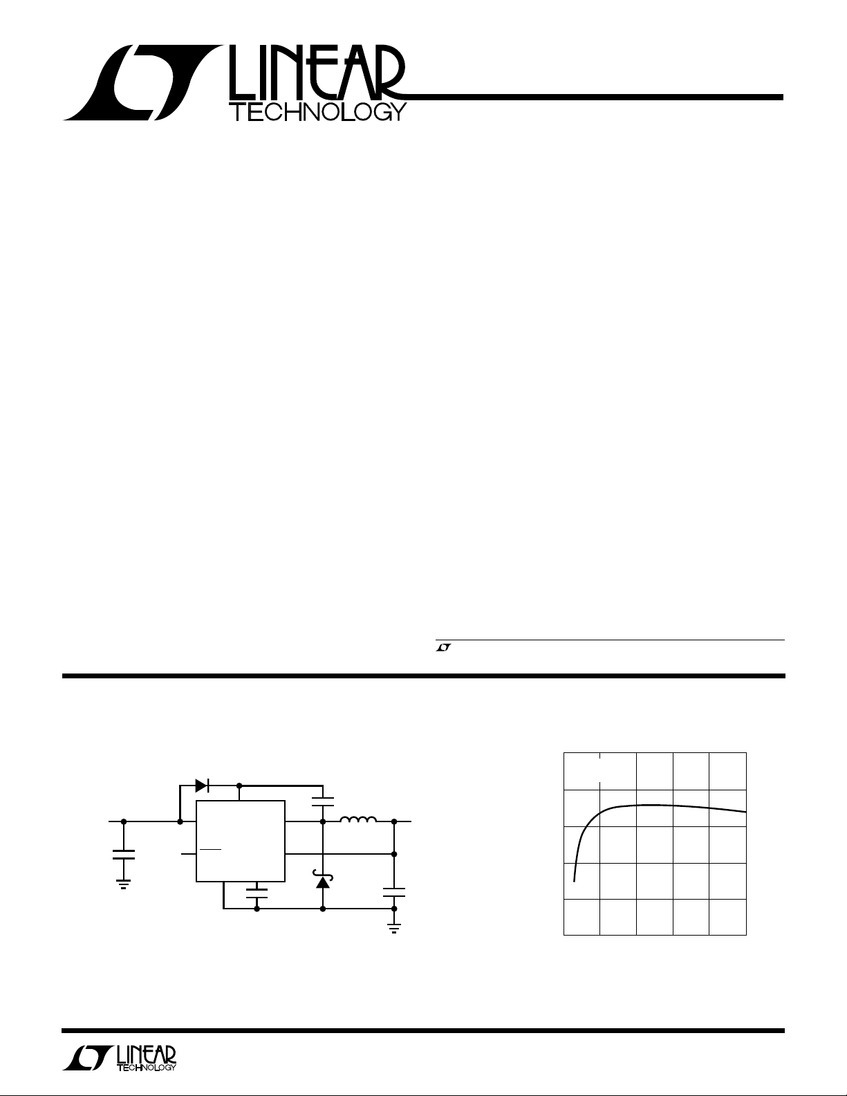
TYPICAL APPLICATION
5V to 3.3V Volt Down Converter
D2†
1N914
BOOST
= ON
V
IN
SHDN
GND V
LT1507-3.3
V
SW
SENSE
C
CC
3.3nF
5V
C3*
47µF
16V
TANTALUM
AVX TPSD477M016R0150 OR SPRAGUE 593D EQUIVALENT.
*
RIPPLE CURRENT RATING ≥ 0.6A
AVX TPSD108M010R0100 OR SPRAGUE 593D EQUIVALENT
**
COILTRONICS CTX5-1. SUBSTITUTION UNITS SHOULD BE RATED
***
AT ≥ 1.25A, USING LOW LOSS CORE MATERIAL
†
SEE BOOST PIN CONSIDERATIONS IN APPLICATIONS INFORMATION
SECTION FOR ALTERNATIVE D2 CONNECTION
+
DEFAULT
(OPEN)
C2
0.1µF
L1***
5µH
D1
1N5818
OUTPUT
3.3V
1.25A
C1**
+
100µF
10V
TANTALUM
100
VIN = 5V
V
OUT
90
80
70
EFFICIENCY (%)
60
50
0
5V to 3.3V Efficiency
= 3.3V
0.25
LOAD CURRENT (A)
0.50
0.75
1.00
1.25
LT1507 • TA02
1
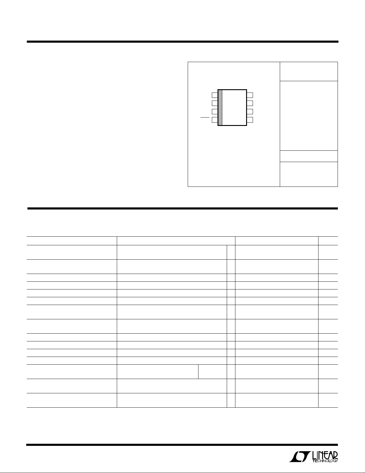
LT1507
1
2
3
4
8
7
6
5
TOP VIEW
V
C
FB/SENSE
GND
SYNC
BOOST
V
IN
V
SW
SHDN
N8 PACKAGE
8-LEAD PDIP
S8 PACKAGE
8-LEAD PLASTIC SO
WW
W
U
ABSOLUTE MAXIMUM RATINGS
Input Voltage ........................................................... 16V
Boost Pin Voltage .................................................... 25V
Shutdown Pin Voltage ............................................... 7V
FB Pin Voltage (Adjustable Part)............................. 3.5V
FB Pin Current (Adjustable Part)............................. 1mA
Sense Voltage (Fixed 3.3V Part) ................................ 5V
Sync Pin Voltage ....................................................... 7V
Operating Ambient Temperature Range
LT1507C.................................................. 0°C to 70°C
LT1507I .............................................. –40°C to 85°C
Max Operating Junction Temperature................... 125°C
Storage Temperature Range ................. –65°C to 150°C
Lead Temperature (Soldering, 10 sec)..................300°C
U
W
PACKAGE/ORDER INFORMATION
ORDER PART
NUMBER
LT1507CN8
LT1507CN8-3.3
LT1507CS8
LT1507CS8-3.3
LT1507IN8
LT1507IN8-3.3
LT1507IS8
LT1507IS8-3.3
T
= 125°C, θJA = 80°C/W TO 120°C/ W (N)
JMAX
= 125°C, θJA = 120°C/W TO 170°C/ W (S)
T
JMAX
DEPENDING ON PC BOARD LAYOUT
Consult factory for Military grade parts.
S8 PART MARKING
1507
15073
1507I
1507I3
U
ELECTRICAL CHARACTERISTICS
TJ = 25°C, VIN = 5V, VC = 1.5V, boost open, switch open unless otherwise specified.
PARAMETER CONDITIONS MIN TYP MAX UNITS
Reference Voltage (Adjustable) 2.39 2.42 2.45 V
All Conditions ● 2.36 2.48 V
Sense Voltage (3.3V) 3.25 3.3 3.35 V
All Conditions ● 3.23 3.37 V
Sense Pin Resistance ● 4.0 6.6 9.5 kΩ
Reference Voltage Line Regulation 4.3V ≤ VIN ≤ 15V ● 0.01 0.03 %/V
FB Input Bias Current ● 0.5 2 µA
Error Amplifier Voltage Gain (Note 8) (Note 1) 150 400
Error Amplifier Transconductance (Note 8) ∆I(V
Pin to Switch Current
V
C
Transconductance 2 A/V
Error Amplifier Source Current VFB = 2.1V or V
Error Amplifier Sink Current VFB = 2.7V or V
VC Pin Switching Threshold Duty Cycle = 0 0.9 V
VC Pin High Clamp VFB = 2.1V or V
Switch Current Limit VC Open, VFB = 2.1V or V
Switch On Resistance (Note 6) ISW = 1.5A, V
Maximum Switch Duty Cycle VFB = 2.1V or V
) = ±10µA 1500 2000 2700 µmho
C
VIN ≥ 5V, V
= 2.9V ● 150 225 320 µA
SENSE
= 3.7V 2 mA
SENSE
= 2.9V 2.1 V
SENSE
= 2.9V DC ≤ 50% ● 1.50 2 3 A
SENSE
= VIN + 5V DC = 80% ● 1.35 3 A
BOOST
= VIN + 5V 0.3 0.4 Ω
BOOST
= 2.9V 90 93 %
SENSE
● 1100 3000 µmho
● 0.5 Ω
● 86 93 %
2
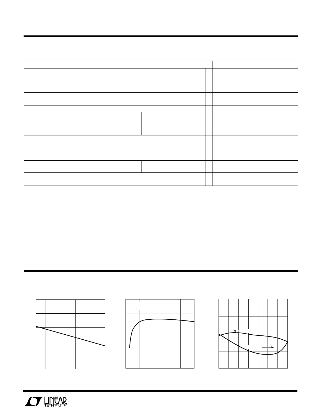
LT1507
JUNCTION TEMPERATURE (°C)
–50
2.44
2.43
2.42
2.41
2.40
100
LT1507 • TPC03
–25 0 25 50 75 125
FEEDBACK VOLTAGE (V)
CURRENT (µA)
2.0
1.5
1.0
0.5
0
VOLTAGE
CURRENT
ELECTRICAL CHARACTERISTICS
TJ = 25°C, VIN = 5V, VC = 1.5V, boost open, switch open unless otherwise specified.
PARAMETER CONDITIONS MIN TYP MAX UNITS
Switch Frequency VC Set to Give 50% Duty Cycle 460 500 540 kHz
–25°C ≤ T
TJ ≤ –25°C 440 570 kHz
Switch Frequency Line Regulation 4.3V ≤ VIN ≤ 15V ● 0.05 0.15 %/V
Frequency Shifting Threshold on FB Pin ∆f = 10kHz ● 0.8 1.0 1.3 V
Minimum Input Voltage (Note 2) ● 4 4.3 V
Minimum Boost Voltage (Note 3) ISW ≤ 1.5A ● 3 3.5 V
Boost Current (Note 4) V
BOOST
Input Supply Current (Note 5) ● 3.8 5.4 mA
Shutdown Supply Current V
SHDN
VSW = 0V, VC Open ● 75 µA
Lockout Threshold VC Open ● 2.3 2.38 2.46 V
Shutdown Threshold V
C
Minimum Synchronizing Amplitude ● 1.5 2.2 V
Synchronizing Frequency Range (Note 7) 580 1000 kHz
≤ 125°C 440 560 kHz
J
= VIN + 5V ISW = 500mA, –25°C ≤ TJ ≤ 125°C1222mA
T
≤ –25°C25mA
I
= 1.5A, –25°C ≤ TJ ≤ 125°C2535mA
SW
J
T
≤ –25°C40mA
J
= 0V, VIN ≤ 12V 15 50 µA
Open Device Shutting Down ● 0.15 0.37 0.70 V
Device Starting Up ● 0.25 0.45 0.70 V
● denotes specifications which apply over the operating temperature
The
range.
Note 1: Gain is measured with a V
clamp level to 200mV below the upper clamp level.
Note 2: Minimum input voltage is not measured directly, but is guaranteed
by other tests. It is defined as the voltage where internal bias lines are still
regulated, so that the reference voltage and oscillator frequency remain
constant. Actual minimum input voltage to maintain a regulated output will
depend on output voltage and load current. See Applications Information.
Note 3: This is the minimum voltage across the boost capacitor needed to
guarantee full saturation of the internal power switch.
Note 4: Boost current is the current flowing into the BOOST pin with the
pin held 5V above input voltage. It flows only during switch ON time.
TYPICAL PERFORMANCE CHARACTERISTICS
1.4
1.2
1.0
0.8
THRESHOLD VOLTAGE (V)
0.6
0.4
C
VC Pin Shutdown Threshold
–25 0 25 50 75 125
–50
JUNCTION TEMPERATURE (°C)
swing equal to 200mV above the low
W
U
Switch Peak Current Limit Feedback Pin Voltage and Current
100
VIN = 5V
= 3.3V
V
OUT
90
100
LT1507 • TPC01
80
70
EFFICIENCY (%)
60
50
0
0.25
0.50
LOAD CURRENT (A)
Note 5: Input supply current is the bias current drawn by the V
pin when
IN
the SHDN pin is held at 1V (switching disabled).
Note 6: Switch ON resistance is calculated by dividing V
to VSW voltage
IN
by the forced current (1.5A). See Typical Performance Characteristics for
the graph of switch voltage at other currents.
Note 7: For synchronizing frequency above 700kHz, with duty cycles
above 50%, external slope compensation may be needed. See Applications
Information.
Note 8: Transconductance and voltage gain refer to the internal amplifier
exclusive of the voltage divider. To calculate gain and transconductance
refer to SENSE pin on fixed voltage parts. Divide values shown by the ratio
/2.42.
V
OUT
0.75
1.00
1.25
LT1507 • TA02
3
LT1507
INPUT VOLTAGE (V)
0
0
INPUT SUPPLY CURRENT (µA)
5
10
15
20
25
30
36912
LT1507 • TPC06
15
V
SHDN
= 0V
FREQUENCY (Hz)
GAIN (µmho)
PHASE (DEG)
3000
2500
2000
1500
1000
500
200
150
100
50
0
–50
100 10k 100k 10M
LT1507 • TPC09
1k 1M
GAIN
PHASE
R
OUT
200k
C
OUT
12pF
V
C
V
FB
× 2e
–3
ERROR AMPLIFIER EQUIVALENT CIRCUIT
R
LOAD
= 50Ω
LOAD CURRENT (mA)
1
5.0
INPUT VOLTAGE (V)
5.5
6.0
6.5
10 100 1000
LT1507 • TPC12
4.5
4.0
3.5
3.0
MINIMUM VOLTAGE
TO START WITH
STANDARD CIRCUIT
MINIMUM VOLTAGE
TO RUN WITH
STANDARD CIRCUIT
MINIMUM INPUT VOLTAGE CAN BE REDUCED
BY ADDING A SMALL EXTERNAL PNP. SEE
APPLICATIONS INFORMATION
W
U
TYPICAL PERFORMANCE CHARACTERISTICS
Shutdown Pin Bias Current
500
CURRENT REQUIRED TO FORCE SHUTDOWN
(FLOWS OUT OF PIN). AFTER SHUTDOWN,
400
CURRENT DROPS TO A FEW µA
300
200
CURRENT (µA)
8
AT 2.38V STANDBY THRESHOLD
(CURRENT FLOWS OUT OF PIN)
4
0
–50
–25 0
25 75
TEMPERATURE (°C)
50 100 125
L11507 • TPC04
Standby and Shutdown Thresholds
2.40
STANDBY
2.36
2.32
0.8
STARTUP
0.4
SHUTDOWN PIN VOLTAGE (V)
0
–50
–25 0
SHUTDOWN
50 100 125
25 75
JUNCTION TEMPERATURE (°C)
Shutdown Supply Current Error Amplifier Transconductance
150
125
100
75
50
INPUT SUPPLY CURRENT (µA)
25
VIN = 10V
2500
2000
1500
1000
500
TRANSCONDUCTANCE (µmho)
Shutdown Supply Current
LT1507 • TPC05
Error Amplifier Transconductance
0
0.1 0.2 0.3 0.4
0
SHUTDOWN VOLTAGE (V)
Frequency Foldback
500
400
300
200
100
0
SWITCHING FREQUENCY (kHz) OR CURRENT (µA)
0
4
SWITCHING
FREQUENCY
FEEDBACK PIN
CURRENT
0.5
1.0
FEEDBACK PIN VOLTAGE (V)
LT1507 • TPC07
0.5
0
–50
0
–25
JUNCTION TEMPERATURE (°C)
50
25
75
100
LT1507 • TPC08
125
Minimum Input Voltage
with 3.3V OutputSwitching Frequency
600
550
500
2.0
LT1507 • TPC10
2.5
1.5
FREQUENCY (kHz)
450
400
–25 0 25 50 75 125
–50
JUNCTION TEMPERATURE (°C)
100
LT1507 • TPC11
W
INPUT VOLTAGE (V)
0
0
CURRENT (A)
0.25
0.50
0.75
1.00
1.25
1.50
36912
LT1507 • TPC15
15
L = 10µH
L = 5µH
L = 20µH
U
TYPICAL PERFORMANCE CHARACTERISTICS
LT1507
Current Limit Foldback
2.5
2.0
1.5
1.0
OUTPUT CURRENT (A)
0.5
*POSSIBLE
UNDESIRED
STABLE POINT
FOR CURRENT
SOURCE LOAD
0
20
0
OUTPUT VOLTAGE (%)
*SEE "MORE THAN JUST VOLTAGE FEEDBACK"
IN APPLICATIONS INFORMATION SECTION
FOLDBACK
CHARACTERISTICS
60
40
RESISTOR LOAD
Boost Pin Current
12
TJ = 25°C
10
8
CURRENT
SOURCE LOAD
MOS LOAD
80
LT1507 • TPC13
100
Maximum Load Current
at V
= 3.3V
1.50
1.25
1.00
0.75
CURRENT (A)
0.50
0.25
OUT
V
L = 10µH
L = 5µH
L = 3µH
L = 2µH
0
4
6 8 10 12
INPUT VOLTAGE (V)
Inductor Core Loss for 3.3V Output
1.0
V
= 3.3V
OUT
= 5V
V
IN
= 1A
I
OUT
0.1
TYPE 52 POWDERED IRON
OUT
= 3.3V
LT1507 • TPC14
Maximum Load Current
at V
= 5V
OUT
14
Switch Voltage Drop
0.8
TJ = 25°C
0.6
6
4
BOOST PIN CURRENT (mA)
2
0
0.25 0.50 0.75 1.00
0
Kool Mµ is a registered trademark of Magnetics, Incorporated.
Metglas is a registered trademark of AlliedSignal Incorporated.
SWITCH CURRENT (A)
1.25
LT1507 • TPC16
CORE LOSS (W)
0.01
PERMALLOY
0.001
1
CORE LOSS IS INDEPENDENT OF LOAD CURRENT
UNTIL LOAD CURRENT FALLS LOW ENOUGH
FOR CIRCUIT TO GO INTO DISCONTINUOUS MODE
®
Kool Mµ
µ = 125
246810
INDUCTANCE (µH)
UUU
PIN FUNCTIONS
BOOST (Pin 1): The BOOST pin is used to provide a drive
voltage, higher than the input voltage, to the internal
bipolar NPN power switch. Without this added voltage the
typical switch voltage loss would be about 1.5V. The
additional boost voltage allows the switch to saturate and
voltage loss approximates that of a 0.3Ω FET structure,
but with a much smaller die area. Efficiency improves from
0.4
SWITCH VOLTAGE (V)
0.2
0
0.25 0.50 0.75 1.00
0
SWITCH CURRENT (A)
1.25 1.50
LT1507 • TPC18
Metglas
®
LT1507 • TPC17
70% for conventional bipolar designs to greater than 85%
for these new parts.
VIN (Pin 2): Input Pin. The LT1507 is designed to operate
with an input voltage between 4.5V and 15V. Under certain
conditions, input voltage may be reduced down to 4V.
Actual minimum operating voltage will always be higher
than the output voltage. It may be limited by switch
5

LT1507
PIN FUNCTIONS
UUU
saturation voltage and maximum duty cycle. A typical
value for minimum input voltage is 1V above output
voltage. Start-up conditions may require more voltage at
light loads. See Minimum Input Voltage for details.
VSW (Pin 3): The switch pin is driven up to the input voltage
in the ON state and is an open circuit in the OFF state. At
higher load currents, pin voltage during the off condition
will be one diode drop below ground as set by the external
catch diode. At lighter loads the pin will assume an
intermediate state equal to output voltage during part of
the switch OFF time. Maximum
switch pin is 1V with respect to the GND pin, so it must
always be clamped with a catch diode to the GND pin.
SHDN (Pin 4): The shutdown pin is used to turn off the
regulator and to reduce input drain current to a few
microamperes. Actually this pin has two separate thresholds, one at 2.38V to disable switching and a second at
0.4V to force complete micropower shutdown. The 2.38V
threshold functions as an accurate undervoltage lockout
(UVLO). This is sometimes used to prevent the regulator
from delivering power until the input voltage has reached
a predetermined level.
negative
voltage on the
SYNC (Pin 5): The SYNC pin is used to synchronize the
internal oscillator to an external signal. It is directly logic
compatible and can be driven with any signal between
10% and 90% duty cycle. The synchronizing range is
equal to
Sychronizing section for details.
FB/SENSE (Pin 7): The feedback pin is used to set output
voltage using an external voltage divider that generates
2.42V at the pin with the desired output voltage. The fixed
voltage (– 3 .3V) parts have the divider included on the chip
and the feedback pin is used as a sense pin connected
directly to the 5V output. Two additional functions are
performed by the feedback pin. When the pin voltage
drops below 1.7V, switch current limit is reduced. Below
1V, switching frequency is also reduced. See More Than
Just Voltage Feedback.
VC (Pin 8): The VC pin is the output of the error amplifier
and the input of the peak switch current comparator. It is
normally used for frequency compensation but can do
double duty as a current clamp or control loop override.
This pin sets at about 1V for very light loads and 2V at
maximum load. It can be driven to ground to shut off the
regulator, but if driven high, current must be limited to 4mA.
initial
operating frequency up to 1MHz. See
W
BLOCK DIAGRAM
The LT1507 is a constant frequency, current mode buck
converter. This means that there is an internal clock and
two feedback loops that control the duty cycle of the power
switch. In addition to the normal error amplifier, there is
a current sense amplifier that monitors switch current on
a cycle-by-cycle basis. A switch cycle starts with an
oscillator pulse which sets the RS flip-flop to turn the
switch on. When switch current reaches a level set by the
inverting input of the comparator, the flip-flop is reset and
the switch turns off. Output voltage control is obtained by
using the output of the error amplifier to set the switch
current trip point. This technique means that the error
amplifier commands current to be delivered to the output
rather than voltage. A voltage fed system will have low
phase shift up to the resonant frequency of the inductor
and output capacitor, then an abrupt 180° shift will occur.
The current fed system will have 90° phase shift at a much
lower frequency, but will not have the additional 90° shift
until well beyond the LC resonant frequency. This makes
it much easier to frequency compensate the feedback loop
and also gives much quicker transient response.
High switch efficiency is attained by using the BOOST pin
to provide a voltage to the switch driver which is higher
than the input voltage, allowing the switch to be saturated.
This boosted voltage is generated with an external capacitor and diode.
Two comparators are connected to the shutdown pin. One
has a 2.38V threshold for undervoltage lockout and the
second has a 0.4V threshold for complete shutdown.
6
 Loading...