

查询LT1500供应商
FEATURES
LT1500/LT1501
Adaptive-Frequency
Current Mode Switching Regulators
U
DESCRIPTION
■
Low Noise Adaptive-Frequency Current Mode
Operation Avoids Low Frequency Noise at
Most Load Currents
■
Can Be Externally Synchronized (LT1500)
■
Micropower Quiescent Current: 200µA
■
Shutdown Current: 8µA Typ
■
Internal Loop Compensation
■
Low-Battery Comparator Active in Shutdown
■
Minimum Input Voltage: 1.8V Typ
■
Additional Negative Voltage Feedback Pin (LT1500)
■
Up to 500kHz Switching Frequency
■
Uses Low Profile, Low Cost Surface Mount Inductors
U
APPLICATIONS
■
Portable Instrumentation
■
Battery Operated Systems
■
PDA’s
■
Standby Power
The LT®1500 is an adaptive-frequency current mode stepup switching regulator with an internal power switch that
is rated up to 700mA. In contrast to pulse skipping
switching regulators, the LT1500 uses a current mode
topology that provides lower noise operation and improved efficiency. Only at very light loads is Burst Mode
TM
activated to give high efficiency and micropower operation. High switching frequency (up to 500kHz) allows very
small inductors to be used, along with ceramic capacitors
if desired.
The LT1500 operates with input voltages from 1.8V to 15V
and has only 200µ A operating current dropping to 8µA in
shutdown. A low-battery comparator is included which
stays alive in shutdown. A second output feedback pin
with negative polarity allows negative output voltages to
be regulated when the switcher is connected up as a Cuk
or a flyback converter.
Two package types are available. The LT1500 comes in a
14-pin SO package, with two options available for fixed
output (3.3V or 5V) or adjustable operation. A reduced
feature part, the LT1501, comes in the smaller 8-pin SO
package with internal frequency compensation. It is also
available in adjustable and fixed output voltage versions.
, LTC and LT are registered trademarks of Linear Technology Corporation.
Burst Mode is a trademark of Linear Technology Corporation.
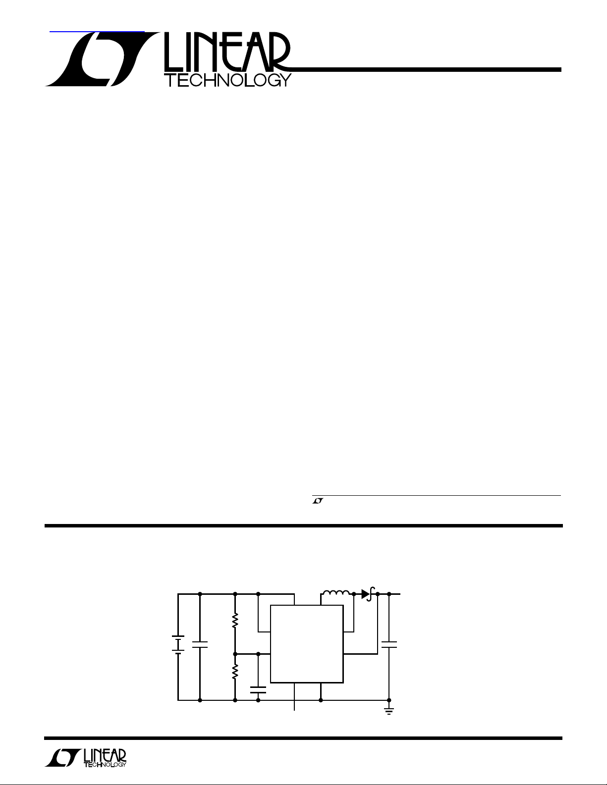
TYPICAL APPLICATION
2 EACH
NiCd OR
ALKALINE
CELLS
+
U
33µF*
6V
2-Cell to 5V Converter
V
301k
1%
301k
1%
(USE EXTERNAL PULL-UP)
IN
SHDN
LT1501-5
LBI
LBO
1nF
LOW-BATTERY FLAG
I
SENSE
GND
22µH
SW
OUT
MBR0520L
†
D1
5V, 200mA
220µF**
+
10V
TANT
AVX, TPSC107M006R0150
*
AVX, TPSD107M010 R0100
**
†
SUMIDA CD73-220, CD54-220
OR CD43-220. SELECT ACCORDING
TO MAXIMUM LOAD CURRENT
LT1500/01 • TA01
1
LT1500/LT1501
1
2
3
4
8
7
6
5
TOP VIEW
FB/OUT
LBI
LBO
SW
SHDN
V
IN
I
SENSE
GND
S8 PACKAGE
8-LEAD PLASTIC SO
WW
W
U
ABSOLUTE MAXIMUM RATINGS
Supply Voltage ........................................................ 20V
Switch Voltage (SW)................................................ 30V
Shutdown Voltage (SHDN) ...................................... 20V
I
Voltage.......................................................... 20V
SENSE
FB Voltage ................................................................. 5V
LBI Voltage................................................................ 5V
LBO Voltage............................................................. 15V
U
W
PACKAGE/ORDER INFORMATION
TOP VIEW
1
1
SHDN
2
V
C
3
V
IN
4
I
SENSE
5
NC
6
GND
7
PGND
14-LEAD PLASTIC SO
T
JMAX
14
13
12
11
10
9
8
S PACKAGE
= 100°C, θJA = 100°C/W
FB
NFB
SS
LBI
LBO
SYNC
SW
SHDN
2
V
C
3
V
IN
4
I
SENSE
5
NC
6
GND
7
PGND
14-LEAD PLASTIC SO
T
= 100°C, θJA = 100°C/W
JMAX
Operating Ambient Temperature Range
Commercial .............................................0°C to 70°C
Industrial ............................................ –40°C to 85°C
Operating Junction Temperature Range
Commercial ...........................................0°C to 100°C
Industrial .......................................... –40°C to 100°C
Storage Temperature Range................. –65°C to 150°C
Lead Temperature (Soldering, 10 sec)..................300°C
U
TOP VIEW
14
(3.3V/5V)
V
OUT
13
SELECT
12
SS
11
LBI
10
LBO
9
SYNC
8
SW
S PACKAGE
T
= 100°C, θJA = 120°C/W
JMAX
ORDER PART NUMBER ORDER PART NUMBER ORDER PART NUMBER
LT1500CS
LT1500IS
LT1500CS-3/5
LT1500IS-3/5
LT1501CS8
LT1501CS8-3.3
LT1501CS8-5
LT1501IS8
LT1501IS8-3.3
LT1501IS8-5
Consult factory for Military grade parts.
ELECTRICAL CHARACTERISTICS
TJ = 25°C, VIN = 2.3V unless otherwise noted.
PARAMETER CONDITIONS MIN TYP MAX UNITS
Feedback/Output Pin Reference Voltage LT1500/LT1501, T
= 25°C 1.240 1.265 1.290 V
J
All Conditions (Note 6) ● 1.235 1.295 V
LT1500-3/5, Select Pin Open 3.230 3.300 3.370 V
All Conditions (Note 6) ● 3.200 3.400 V
LT1500-3/5, Select Pin Grounded 4.900 5.000 5.100 V
All Conditions (Note 6) ● 4.85 5.15 V
Reference Voltage Line Regulation VIN = 2.3V to 15V ● 0.02 0.06 %/V
Feedback Pin Bias Current ● 30 100 nA
2

LT1500/LT1501
ELECTRICAL CHARACTERISTICS
PARAMETER CONDITIONS MIN TYP MAX UNITS
Internal Divider Current LT1500-3.3/LT1501-3.3
LT1500-5/LT1501-5 ● 33 45 µA
Operating Quiescent Current V
Supply Current in Shutdown V
Shutdown Pin Threshold ● 0.4 1.1 V
Shutdown Pin Input Current V
Input Start-Up Voltage V
Undervoltage Lockout Light Load 1.8 V
Power Switch
Switch On Resistance ISW = 0.7A (Note 2) ● 0.50 0.72 Ω
Peak Switch Current (Note 3) ● 0.7 0.85 1.3 A
Switch Breakdown Voltage ISW = 100µA ● 30 45 V
Switch Leakage Current V
Switch Turn-On Delay (Note 5) 800 ns
Switch Turn-Off Delay (Note 5) 400 ns
Current Sense Resistor ● 0.28 0.42 Ω
Low-Battery Comparator
Low-Battery Threshold Falling Edge ● 1.20 1.24 1.28 V
Threshold Hysteresis 20 mV
LBI Input Bias Current ● 20 50 nA
LBO Output Low State V
LBO Leakage Current V
LT1500 Functions
SYNC Pin Bias Current V
SYNC Pin Threshold ● 0.4 1.3 V
Error Amplifier Transconductance 600 µmho
VC Pin Source Current 20 µA
VC Pin High Clamp Voltage 1.20 1.26 1.32 V
NFB Reference Voltage FB Pin Open ● 1.230 1.265 1.300 V
NFB Pin Bias Current ● 12 20 µA
NFB to FB Transconductance Note 4 10,000 µmho
Soft Start Bias Current Current Flows Out of Pin ● 247 µA
≤ 5V, V
IN
VIN = 15V ● 320 µA
≤ 0.2V, Fixed Voltages (Note 7)
SHDN
≥ 0°C ● 815 µA
T
J
T
< 0°C20µA
J
= 2.3V ● 310 µA
SHDN
= V
SHDN
Full Load 2.0 2.1 V
SW
VSW = 20V ● 0.3 10 µA
LBI
I
SINK
LBI
SYNC
IN
TJ ≥ 0°C ● 2.0 2.1 V
TJ < 0°C 2.2 V
= 5V ● 0.2 5 µA
= 1.2V, I
= 2mA ● 0.3 0.5 V
= 1.3V, V
= 3.3V ● 15 35 µA
TJ = 25°C, VIN = 2.3V unless otherwise noted.
● 22 30 µA
= 2.3V (Note 1) ● 200 280 µA
SHDN
= 100µA ● 0.1 0.25 V
SINK
≤ 15V ● 2 µA
LBO
3
LT1500/LT1501
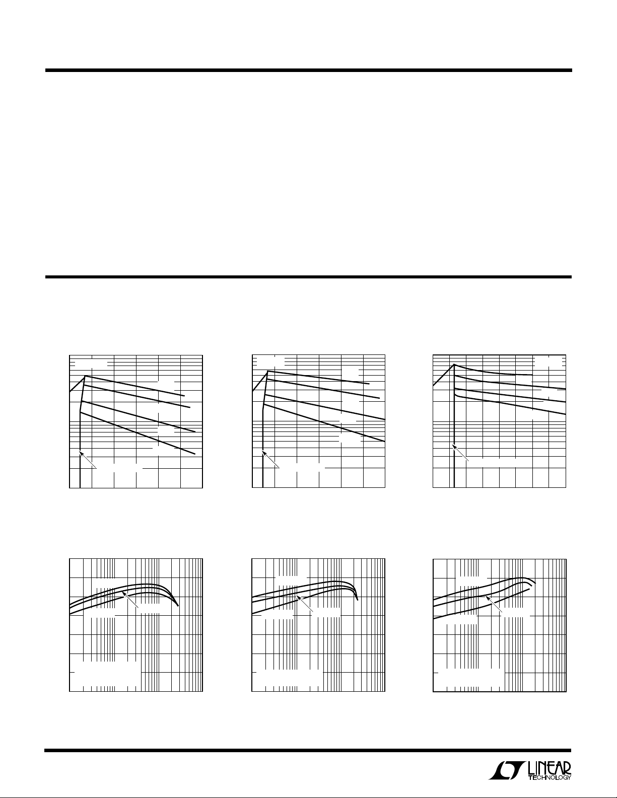
LOAD CURRENT (mA)
0255075
FREQUENCY (kHz)
1000
100
10
100 125 150 175 200
LTC1500/01 • TPC22
10µH
50µH
20µH
100µH
BURST REGION
VIN = 5V
ELECTRICAL CHARACTERISTICS
The ● denotes specifications which apply over the full operating
temperature range.
Note 1: Feedback pin or output is held sightly above the regulated value to
force the V
node low and switching to stop.
C
Note 2: See Typical Performance Characteristics for graph of Guaranteed
Switch Voltage vs Saturation Voltage.
Note 3: Peak switch current is the guaranteed minimum value of switch
current available in normal operation. Highest calculated switch current at
full load should not exceed the minimum value shown.
Note 4: Loading on FB pin will affect NFB reference voltage. ∆V
= IFB/gm.
NFB
Do not exceed 10µA loading on FB when NFB is being used.
Note 5: This is the delay between sense pin current reaching its upper or
lower threshold and switch transition. Switch delay times cause peak-to-
W
U
peak inductor current to increase and therefore switching frequency to be
low. This effect will be significant for frequencies above 100kHz. See
Application Information and Typical Performance Characteristics.
Note 6: Reference voltage under all conditions includes V
all loads and full temperature range.
Note 7: As with all boost regulators the output voltage of the LT1500
cannot fall to less than input voltage because of the path through the catch
diode. This means that the output voltage divider on adjustable parts will
still be generating feedback voltage at the FB pin (fixed voltage parts have
an internal switch to disconnect the divider in shutdown). If the voltage on
FB is greater than 0.6V in shutdown, the internal error amplifier will draw
current that adds to shutdown current. See graph of Shutdown Current vs
FB voltage in Typical Performance Characteristics.
TYPICAL PERFORMANCE CHARACTERISTICS
Switching Frequency
(3.3V Output)
1000
VIN = 2.3V
100
FREQUENCY (kHz)
10µH
20µH
50µH
100µH
Switching Frequency (5V Output)
1000
VIN = 3V
100
FREQUENCY (kHz)
50µH
100µH
10µH
20µH
= 2.1V to 15V,
IN
Switching Frequency (12V Output)
EFFICIENCY (%)
BURST REGION
10
0 50 100
LOAD CURRENT (mA)
Efficiency (3.3V Output)
100
90
80
70
60
50
40
30
L = 100µH
L = 10µH
TJ = 25°C
= 2.3V
V
IN
LOW LOSS INDUCTOR
1
LOAD CURRENT (mA)
10 100 1000
150 200 250 300
LTC1500/01 • TPC20
L = 33µH
LTC1500/01 • TPC17
BURST REGION
10
0 50 100
LOAD CURRENT (mA)
Efficiency (5V Output)
100
90
80
70
60
EFFICIENCY (%)
50
40
30
L = 100µH
L = 10µH
VIN = 3V
LOW LOSS INDUCTOR
1
10 100 1000
LOAD CURRENT (mA)
150 200 250 300
LTC1500/01 • TPC21
L = 33µH
LTC1500/01 • TPC18
Efficiency (12V Output)
100
90
80
70
60
EFFICIENCY (%)
50
40
30
L = 100µH
L = 10µH
VIN = 5V
LOW LOSS INDUCTOR
1
10 100 1000
LOAD CURRENT (mA)
L = 33µH
LTC1500/01 • TPC19
4

W
I
LOAD
= 50mA
I
LOAD
= 10mA
INPUT VOLTAGE (V)
0
EFFICIENCY (%)
100
90
80
70
60
50
40
2
468
LT1500/01 • TPC13
10 12
TJ = 25°C
L = 33µH
LOW LOSS INDUCTOR
U
TYPICAL PERFORMANCE CHARACTERISTICS
LT1500/LT1501
Efficiency (3.3V Output)
100
90
80
70
EFFICIENCY (%)
60
TJ = 25°C
50
L = 33µH
LOW LOSS INDUCTOR
40
1.75
I
LOAD
2.25 2.50 2.75
2.00
INPUT VOLTAGE (V)
= 100mA
Inductor Copper Loss
(3.3V Output)
10
R = 1Ω
1
I
LOAD
R = 0.5Ω
R = 0.2Ω
R = 0.1Ω
= 10mA
3.00 3.25
LT1500/01 • TPC11
Efficiency (5V Output)
100
I
= 10mA
90
80
70
EFFICIENCY (%)
60
50
40
2.0
LOAD
TJ = 25°C
L = 33µH
LOW LOSS INDUCTOR
3.0 3.5 4.0
2.5
INPUT VOLTAGE (V)
I
LOAD
= 100mA
Inductor Copper Loss (5V Output)
10
VIN = 3V
1
R = 1Ω
R = 0.5Ω
4.5 5.0
LT1500/01 • TPC12
R = 0.2Ω
R = 0.1Ω
Efficiency (12V Output)
Inductor Copper Loss
(12V Output)
10
VIN = 5V
1
R = 1Ω
R = 0.5Ω
R = 0.2Ω
EFFICIENCY LOSS (%)
VIN = 2.3V
0.1
0 50 100
LOAD CURRENT (mA)
Maximum Load Current
(3.3V Output)
600
500
400
300
200
OUTPUT CURRENT (mA)
100
0
1.50
2.00 2.25 2.50
1.75
INPUT VOLTAGE (V)
150 200 250 300
LT1500/01 • TPC14
L ≥ 33µH
L = 10µH
2.75 3.00
LT1500/01 • TPC08
EFFICIENCY LOSS (%)
0.1
600
500
400
300
200
OUTPUT CURRENT (mA)
100
0
0 50 100
150 200 250 300
LOAD CURRENT (mA)
Maximum Load Current
(5V Output)
L ≥ 33µH
L = 10µH
2.0
3.0 3.5 4.0
2.5
INPUT VOLTAGE (V)
LT1500/01 • TPC15
4.5 5.0
LT1500/01 • TPC09
EFFICIENCY LOSS (%)
0.1
600
500
400
300
200
OUTPUT CURRENT (mA)
100
0
0255075
100 125 150 175 200
LOAD CURRENT (mA)
Maximum Load Current
(12V Output)
L = 33µH
L = 100µH
L = 10µH
0
468
2
INPUT VOLTAGE (V)
LTC1500/01 • TPC16
10 12
LT1500/01 • TPC10
5

LT1500/LT1501
AVERAGE SWITCH CURRENT
0
220
200
180
160
140
120
100
80
0.3 0.5
LT1500/01 • TPC07
0.1 0.2
0.4 0.6 0.7
PEAK-TO-PEAK INDUCTOR CURRENT
VIN = 3.3V
V
OUT
= 5V
L
= 50µH
NOTE THAT RIPPLE CURRENT
INCREASES WITH SMALLER
INDUCTORS DUE TO
PROPAGATION DELAY
IN THE CURRENT
COMPARATOR
W
U
TYPICAL PERFORMANCE CHARACTERISTICS
Burst Mode Threshold
120
TJ = 25°C
LOAD CURRENT IS
100
REDUCED UNTIL Burst
Mode OPERATION STARTS
80
60
40
LOAD CURRENT (mA)
20
V
= 3.3V
OUT
V
= 5V
OUT
V
= 12V
OUT
Switch Saturation Voltage
1.0
TJ = 25°C
0.8
0.6
0.4
SWITCH VOLTAGE (V)
0.2
Peak-to-Peak Inductor Ripple
Current
0
0
468
2
INPUT VOLTAGE (V)
10 12
LT1500/01 • TPC01
0
0.2
0
SWITCH CURRENT (A)
0.4
0.6
0.8
LT1500/01 • TPC06
1.0
Low-Battery Output Saturation
VoltageQuiescent Input Supply Current
400
TJ = 25°C
OR V
V
350
FB
SO THAT Burst Mode
OPERATION IS ACTIVATED.
300
DOES NOT INCLUDE
OUTPUT DIVIDER CURRENT
250
200
150
SUPPLY CURRENT (µA)
100
50
0
510 20
0
HELD 5% HIGH,
OUT
INPUT VOLTAGE (V)
15
25
LT1500/01 • TPC04
0.6
TJ = 25°C
V
LBI
0.5
0.4
0.3
VOLTAGE (V)
0.2
0.1
0
0
≤ 1.2V
234
1
SINK CURRENT (mA)
56
LT1500/01 • TPC02
Shutdown Input Current vs
Input Current in Shutdown
20
TJ = 25°C
= 0V
V
SHDN
16
12
8
CURRENT (µA)
4
0
5
0
INPUT VOLTAGE (V)
15
20
10
25
LT1500/01 • TPC03
Feedback Pin Voltage
140
TJ = 25°C
= 5V
V
120
IN
ADJUSTABLE PARTS ONLY.
FIXED VOLTAGE PARTS DO
100
NOT SHOW SHUTDOWN
CURRENT INCREASE WITH
80
60
CURRENT (µA)
40
20
0
0
FEEDBACK VOLTAGE
0.2 0.4
FEEDBACK PIN VOLTAGE (V)
0.8 1.2 1.4
0.6 1.0
LT1500/01 • TPC05
6

UUU
PIN FUNCTIONS
LT1500/LT1501
SHDN: Logic Level Shutdown Pin.
high (> 1.1V) for the regulator to run
directly to VIN, even with VIN = 18V. The low-battery
detector remains active in shutdown, but all other circuitry
is turned off.
VIN: This pin supplies power to the regulator and is
connected to one side of the inductor sense resistor. It
should be bypassed close to the chip with a low ESR
capacitor.
I
: This is one end of the internal inductor-current
SENSE
sense resistor. With most applications, only the external
inductor is tied to this pin.
GND: This pin carries only low level current in the LT1500,
but it carries full switch current in the LT1501. The
negative end of the input bypass capacitor should be
connected close to this pin and the pin should go directly
to the ground plane with the LT1501.
PGND (LT1500 Only): This pin is the emitter of the internal
NPN power switch. Connect it directly to the ground plane.
This pin must be held
. SHDN can be tied
NFB/SELECT (LT1500 Only): NFB is a second feedback
node used to regulate a negative output voltage. Negative
output voltages can be generated by using a transformer
flyback circuit, a Cuk converter or a capacitor charge pump
added to a boost converter. The regulating point for NFB
is 1.265V and the internal resistance to ground is 100kΩ.
External divider current should be 300µA or greater to
avoid negative output voltage variations due to production
variations in the internal resistor value. FB should be left
open when using NFB.
On fixed voltage parts, NFB is replaced with Select. The
Select pin is used to set output voltage at either 3.3V or 5V.
VC (LT1500 Only): This is the output of the error amplifier
and the input to the current comparator. The VC pin voltage
is about 700mV at very light loads and about 1.2V at full
load. An internal comparator detects when the VC voltage
drops below about 750mV and shuts down the current
comparator and the power switch biasing to reduce quiescent current. This forces the regulator to operate in Burst
Mode operation.
SW: This is the collector of the internal NPN power switch.
To avoid EMI and overvoltage spikes, keep connections to
this pin very short.
LBI: This is the input to the low-battery detector with a
threshold of 1.24V. Maximum pin voltage is 5V. Bypass
LBI with a small filter capacitor when used. If unused, tie
LBI to ground. The low-battery detector remains active in
shutdown.
LBO : This is the open collector output of the low-battery
detector. It will sink up to 2mA. Leave open if not used.
FB/V
a regulating point of 1.265V and a typical bias current of
30nA. Bias current is reduced with a canceling circuit, so
bias current could flow in either direction. FB is replaced
with V
internal divider that is connected to the internal FB node.
A switch disconnects the divider in shutdown so that the
divider current does not load VIN through the inductor and
catch diode.
: FB is the inverting input to the error amplifier with
OUT
on fixed voltage parts. V
OUT
is the top of an
OUT
SYNC (LT1500 Only): This is a logic level input used to
synchronize switching frequency to an external clock. The
sync signal overrides the internal current comparator and
turns the switch on. Minimum sync pulse width should be
50ns and maximum width should be 300ns. A continuous
high sync signal will force the power switch to stay on
indefinitely and current will increase without limit. Don’t
do this!
SS (LT1500 Only): This is the soft start function using the
base of a PNP transistor whose emitter is tied to the VC pin.
Grounding SS will turn off switching by pulling VC low. A
capacitor tied from SS to ground will force VC to ramp up
slowly during start-up at a rate set by the capacitor value
and the internal 4µ A pull-up current. An external resistor
must be used to reset the capacitor voltage completely to
0V at power down.
7

LT1500/LT1501
BLOCK DIAGRAM
LBI
+
–
1.24V
W
INSYNCLBO
I
SENSE
R
SENSE
Rh
0.28Ω
18mV
–
+
OUTPUT
+
0.75V
–
SHDN
BIAS
COMPARATOR
1.265V
REFERENCE
100k
BURST
+
+
ERROR AMP
–
–
100k
NEGATIVE
ERROR AMP
+
FBNFB GND
U
150pF
WUU
APPLICATIONS INFORMATION
CURRENT
COMPARATOR
SW
FIXED
HYSTERESIS
I
1
VARIABLE
HYSTERESIS
I
2
S1
V
C
Q1
PGND
R1
R2
LTC1500/01 • BD
OPERATION (SEE BLOCK DIAGRAM)
The LT1500 uses a current mode architecture without the
need for an internal oscillator. Switching frequency is
determined by the value of the external inductor used. This
technique allows the selection of an operating frequency
best suited to each application and considerably simplifies
the internal circuitry needed. It also eliminates a
subharmonic oscillation problem common to all fixed
frequency (clocked) current mode switchers. In addition,
it allows for high efficiency micropower operation while
maintaining higher operating frequencies. Because the
power switch (Q1) is grounded, the basic topology used
8
will normally be a boost converter with output voltage
always higher than the input voltage. Special topologies
such as the SEPIC, flyback and Cuk converter can also be
used when the output voltage may not always be higher
than the input or when full shutdown of the output voltage
is needed. Operation as a boost converter is as follows.
Assume that inductor current is continuous, meaning that
it never drops to zero. When the switch is on, inductor
current will increase with voltage across the inductor
equal to VIN. When the switch is off inductor current will
decrease with inductor voltage equal to V
OUT
– VIN.
Switching frequency will be determined by the inductor

LT1500/LT1501
U
WUU
APPLICATIONS INFORMATION
value, the peak-to-peak inductor current (set internally)
and the values for VIN and V
output voltage in continuous mode by adjusting the average value of inductor current while maintaining the peakto-peak value of the current relatively constant, hence, the
name “current mode architecture.”
The LT1500 sets the peak-to-peak value of switch current
internally to establish operating frequency. This peak-topeak value is scaled down somewhat at light load currents
to avoid as long as possible the characteristic of other
micropower converters wherein their switching frequency
drops very low (into the audio range) at less than full load
currents. At extremely light loads, even the LT1500 can no
longer maintain higher frequency operation, and utilizes a
Burst Mode operation to control output voltage.
Details of Continuous Mode Operation
At the start of a switch cycle, inductor current has decreased to the point where the voltage across R
less than the internally generated voltage across Rh. This
causes the current comparator output to go high and turn
on the switch. At the same time, extra current is added to
Rh via S1 to create hysteresis in the trip point of the
comparator. This extra current is composed of a fixed
amount (I1), and an amount proportional to average
inductor current (I2). The presence of a variable I2 increases switching frequency at lighter loads to extend the
load current range where high frequency operation is
maintained and no Burst Mode operation exists.
With the switch turned on, inductor current will increase
until the voltage drop across R
voltage across Rh. Then the comparator output will go
low, the switch will turn off and the current through Rh will
be switched back to its lower value. Inductor current will
decrease until the original condition is reached, completing one switch cycle.
Control of output voltage is maintained by adjusting the
continuous current flowing through Rh. This affects both
upper and lower inductor current trip levels at the same
time. Continuous Rh current is controlled by the error
amplifier which is comparing the voltage on the Feedback
pin to the internal 1.265V reference. An internal frequency
. The LT1500 controls
OUT
SENSE
is equal to the higher
SENSE
is
compensation capacitor filters out most the ripple voltage
at the amplifier output.
Operation at Light Loads
At light load currents the lower trip level (switch turn-on)
for inductor current drops below zero. At first glance, this
would seem to initiate a permanent switch off-state because the inductor current cannot reverse in a boost
topology. In fact, what happens is that output voltage
drops slightly between switch cycles, causing the error
amplifier output to increase and bring the current trip level
back up to zero. The switch then turns back on and
inductor current increases to a value set by I1 (I2 is near
zero at this point). The switch then turns off, and the
inductor energy is delivered to the output, causing it to rise
back up slightly. One or more switch cycles may be needed
to raise the output voltage high enough that the amplifier
output drops enough to force a sustained switch off
period. The output voltage then slowly drops back low
enough to cause the amplifier output to rise high enough
to initiate a switch turn-on. Switching operation now
consists of a series of bursts where the switch runs at
normal frequency for one or more cycles, then turns off for
a number of cycles. This Burst Mode operation is what
allows the LT1500 to have micropower operation and high
efficiency at very light loads.
Saving Current in Burst Mode Operation
Internal current drain for the LT1500 control circuitry is
about 400µA when everything is operating. To achieve
higher efficiency at extremely light loads, a special operating mode is initiated when the error amplifier output is
toward the low end of its range. The adaptive bias circuit
comparator detects that the error amplifier output is below
a predetermined level and turns off the current comparator
and switch driver biasing. This reduces current drain to
about 200µA, and forces a switch off state. Hysteresis in
the comparator forces the device to remain in this
micropower mode until the error amplifier output rises up
beyond the original trip point. The regulated output voltage will fall slightly over a relatively long period of time
(remember that load current is very low) until the error
amplifier output rises enough to turn off the adaptive bias
9

LT1500/LT1501
U
WUU
APPLICATIONS INFORMATION
mode. Normal operation resumes for one or more switch
cycles and the output voltage increases until the error
amplifier output falls below threshold, initiating a new
adaptive bias shutdown.
DESIGN GUIDE
Selecting Inductor Value
Inductor value is chosen as a compromise between size,
switching frequency, efficiency and maximum output current. Larger inductor values become physically larger but
provide higher output current and give better efficiency
(because of the lower switching frequency). Low inductance minimizes size but may limit output current and the
higher switching frequency reduces efficiency.
The simplest way to handle these trade-offs is to study the
graphs in the Typical Performance Characteristics section. A few minutes with these graphs will clearly show the
trade-offs and a value can be quickly chosen that meets the
requirements of frequency, efficiency and output current.
This leaves only physical size as the final consideration.
The concern here is that for a given inductor value, smaller
size usually means higher series resistance. The graphs
showing efficiency loss vs inductor series resistance will
allow a quick estimate of the additional losses associated
with very small inductors.
One final consideration is inductor construction. Many
small inductors are “open frame ferrites” such as rods or
barrels. These geometries do not have a closed magnetic
path, so they radiate significant B fields in the vicinity of the
inductor. This can affect surrounding circuitry that is
sensitive to magnetic fields. Closed geometries such as
toroids or E-cores have very low stray B fields, but they are
larger and more expensive (naturally).
Catch Diode
The catch diode in a boost converter has an average
current equal to output current, but the peak current can
be significantly higher. Maximum reverse voltage is equal
to output voltage. A 0.5A Schottky diode like MBR0520L
works well in nearly all applications.
Input Capacitor
Input capacitors for boost regulators are less critical than
the output capacitor because the input capacitor ripple
current is a simple triwave without the higher frequency
harmonics found in the output capacitor current. Peak-topeak current is less than 200mA and worst-case RMS
ripple current in the input capacitor is less than 70mA.
Input capacitor series resistance (ESR) should be low
enough to keep input ripple voltage to less than 100mV
This assumes that the capacitor is an aluminum or tantalum type where the capacitor reactance at the switching
frequency is small compared to the ESR.
C
≥
A typical input capacitor is a 33µ F, 6V surface mount solid
tantalum type TPS from AVX. It is a “C” case size, with
0.15Ω maximum ESR. Some caution must be used with
solid tantalum input capacitors because they can be damaged with turn-on surge currents that occur when a low
impedance power source is hot-switched to the input of
the regulator. This problem is mitigated by using a capacitor with a voltage rating at least twice the highest expected
input voltage. Consult with the manufacturer for additional
guidelines.
If a ceramic input capacitor is used, different design
criteria are used because these capacitors have extremely
low ESR and are chosen for a minimum number of
microfarads.
C Ceramic
()
f = switching frequency
A typical unit is an AVX or Tokin 3.3µF or 4.7µF.
Output Capacitor
Output ripple voltage is determined by the impedance of
the output capacitor at the switching frequency. Solid
tantalum capacitors rated for switching applications are
recommended. These capacitors are essentially resistive
at frequencies above 50kHz, so ESR is the important factor
in determining ripple voltage. A typical unit is a 220µ F, 10V
2
π
f ESR
()( )
1
=
f
4
P-P
.
10

LT1500/LT1501
U
WUU
APPLICATIONS INFORMATION
type TPS from AVX, or type 595D from Sprague. These
have an ESR of 0.06Ω in a “E” case size. At lower output
current levels, a 100µF unit in a “D” case size may be
sufficient. Output ripple voltage can be calculated from:
V ESR
RIPPLE
=+
0112.
IV
.
()( )
OUT OUT
V
IN
Loop frequency stability is affected by the characteristics
of the output capacitor. The ESR of the capacitor should be
very low, and the capacitance must be large (> 200µ F) to
ensure good loop stability under worst-case conditions of
low input voltage, higher output voltages, and high load
currents. The 14-pin LT1500 can use external frequency
compensation on the VC pin to give good loop stability with
smaller output capacitors. See Loop Stability section for
details.
Precautions regarding solid tantalum capacitors for input
bypassing do not apply to the output capacitor because
turn-on surges are limited by the inductor and discharge
surges do not harm the capacitors.
M
1 1 265
.
R
()
12 1 265
–.
=
k2
118=
Note that there is an internal switch that disconnects the
internal divider for fixed 3.3V and 5V parts in shutdown.
This prevents the divider from adding to shutdown current. Without this switch, shutdown current increases
because of the divider current directly, but even more so
if the FB pin is held above 0.6V by the divider. See graphs
in Typical Performance Characteristics.
= 12V
V
OUT
R1
FB
–
ERROR
AMPLIFIER
Figure 1. External Voltage Divider
+
1.265V
1M
1%
R2
118K
1%
LTC1500/01 • F01
Selectable Output (Fixed Voltage Parts)
Setting Output Voltage
Preset 3.3V and 5V parts are available. For other voltage
applications the adjustable part uses an external resistor
divider to set output voltage. Bias current for the feedback
(FB) pin is typically ±30nA (it is internally compensated).
Thevenin divider resistance should be 100kΩ or less to
keep bias current errors to a minimum. This leads to a
value for R1 and R2 (see Figure 1) of:
kV
100
Ω
()
R
1
=
R
2
=
V
OUT
Example: V
100 12
R
OUT
V
1 265
.
R
1 1 265
.
()
1 265
–.
= xxV
OUT
k
Ω
1 265
.
()
=
949=
k1
) (use 1M
The Select pin (available only on LT1500-3/5) allows the
user to select either a 3.3V or 5V output. Floating the pin
sets output voltage at 3.3V and grounding the pin sets
output voltage at 5V. The equivalent circuit of the Select
pin function is shown in Figure 2.
V
OUT
204k
–
ERROR
AMPLIFIER
Figure 2. Schematic of Select Pin Function
+
1.265V
GND
Note that there is a switch in series with the V
69k
58k
SELECT
LTC1500/01 • F02
pin. This
OUT
switch is turned off in shutdown to eliminate shutdown
current drawn by the voltage divider. For adjustable parts
11

LT1500/LT1501
U
WUU
APPLICATIONS INFORMATION
with an external divider no switch exists and the divider
current remains. There may be additional current drawn
by the adjustable LT1500 in shutdown if the divider
voltage at the feedback node exceeds 0.6V. See Typical
Performance Characteristics.
Loop Stability
The LT1501 is internally compensated since the device
has no spare pin for a compensation point. The LT1500
brings out the VC pin to which an external series R
network is connected. This provides roll-off for the error
amplifier, ensuring overall loop stability. Typical values
when using tantalum output capacitors are 1000pF and
100kΩ.
Transient response of Figure 3’s circuit with a 30mA to
100mA load step is detailed in Figure 4. The maximum
output disturbance is approximately 20mV. The “splitting”
of the V
due to ESR of C
trace when load current increases to 100mA is
OUT
. C
OUT
can be replaced by a ceramic
OUT
unit, which has lower ESR, size and cost. Figure 5 shows
transient response to the same 30mA to 100mA load step,
with C
= 15µ F ceramic, CC = 2200pF and RC = 10k. The
OUT
maximum output disturbance in this case is 100mV.
C
Low-Battery Detector
The low-battery detector is a combined reference and
comparator. It has a threshold of 1.24V with a typical input
bias current of 20nA. In a typical application a resistor
divider is connected across the battery input voltage with
the center tap tied to Low Battery Input (LBI), see Figure
6. The suggested parallel resistance of the divider is 150k
V
COMP
500mV/DIV
V
OUT
20mV/DIV
AC COUPLED
I
LOAD
100mA
30mA
I
L
500mA/DIV
500µs/DIV
Figure 4. Transient Response of LT1500 with RC = 100k,
CC = 1000pF and C
V
COMP
500mV/DIV
= 220µF. V
OUT
Disturbance is 20mV
OUT
VIN
2V
SHDN
*TANTALUM = AVX TPS SERIES
CERAMIC = TOKIN 1E156ZY5U
Figure 3. LT1500 2V to 5V Converter
V
IN
LT1500
GND
I
SENSE
PGND
33µH
CTX33-1
SW
FB
V
C
MBR0520L
RC
100k
CC
1000pF
1M
332k
100pF
V
OUT
5V
+
C
OUT
220µF
LT1500/01 • F03
*
V
OUT
50mV/DIV
AC COUPLED
100mA
I
LOAD
30mA
I
L
500mA/DIV
200µs/DIV
Figure 5. Transient Response of LT1500 with RC = 10k, CC =
2200pF and C
=15µF Ceramic. V
OUT
R3
301k
1%
R4
274k
1%
V
LBI LBO
GND
R5
10M
IN
LT1500
LT1501
LT1500/01 • F06
Disturbance is 100mV
OUT
V
CC
470k
PULL-UP RESISTOR
SHOULD BE AT LEAST
FIVE TIMES SMALLER THAN
R5 TO ENSURE LBO
HIGH STATE
Figure 6. Low Battery Detection
12

LT1500/LT1501
R
kM
Mk
4
301 10 1 24
10 2 5 1 24 301 5 1 24
=
()()()
−
()
+−
()
=
.
.. .
272k (Use 274k 1%)
ff
f
fV
VV
SYNC NATURAL
SYNC
NATURAL OUT
OUT IN
>
<
()
–
(Use Minimum V )
IN
U
WUU
APPLICATIONS INFORMATION
and it should be no more than 300k to keep bias current
errors under 1%, giving:
RV
()
R
R
V
BAT
R
DIV
There is about 20mV of hysteresis at the LBI pin. Hysteresis can be increased by adding a resistor (R5) from the
output (LBO) back to LBI. This resistor can be calculated
from the following equation, but note that the equation for
R4 will have to be changed when R5 is added.
R
VCC = supply voltage for LBO pull-up resistor
DIV BAT
3
=
124
.
R
3124
()
=
4
V
–.
BAT
= low battery voltage
= Thevenin divider resistance = R3 in parallel with R4
5
=
VmVV
() ()
HYST BAT
V
.
124
RV
3
()
CC
17
–
The total divider resistance will be 274k + 301k = 575k, and
this will draw about 7µA from a fully charged battery.
Synchronizing
The SYNC pin on the LT1500 can be used to synchronize
switching frequency to an external clock. The pin should
be driven with a 50ns to 300ns pulse which will trigger the
switch to an on state. There is a fairly restricted range over
which synchronizing will work, because the period between
sync pulses must be greater than the natural on-time of
the regulator when it is running unsynchronized, and the
sync frequency must be greater than the unsynchronized
switching frequency. This puts the following restrictions
on synchronized operation:
V
= desired hysteresis at the battery
HYST
R4 (When R5 is Used)=
124
R3 R5
5 1 24 3 1 24
The LBO pin is open collector. The external pull-up resistor
value is determined by user needs. Generally the resistor
is 100k to 1M to keep current drain low, but the LBO pin
can sink several milliamperes if needed.
Example: low battery voltage = 2.5V, desired hysteresis =
200mV, VCC = 5V.
Use R
R
3
R
5
−
()
BAT CC
DIV
150 2 5
=
=
() ()
..RV RV
= 150k
.
k
()
.
124
301 5
.–. .
02 001725
.
()( )
+−
()
k (use 301k, 1%)
302
=
kV
()
=
9
.56M (Use 10M)
f
NATURAL
quency of the regulator. It is a function of load current, so
a careful check must be done to ensure that the above
conditions are met under all load and input voltage conditions.
Soft Start (SS)
The LT1500 can be soft started by connecting a capacitor
to the SS pin. This pin is the base of a PNP transistor
whose emitter is tied to the VC pin. Soft start action will
occur over the range of 0V to 0.8V on the SS pin and the
pin is clamped at 1.2V with an internal clamp. An internal
4µ A pull-up current and the external capacitor value
determine soft start time. In a typical application a 0.22µ F
capacitor is sufficient to limit input surges and prevent
output overshoot, even with overcompensation on the V
pin. Output voltages greater than 6V with very large output
is the natural unsynchronized switching fre-
C
13

LT1500/LT1501
P
W
TOTAL
=
()()()
−
()
()
+
−
()
+
()
()
=+ + =
015 072 5 5 22220155 22
30
0 42 0 15 5
22
0 47 0 014 0 049 0 11
2
2
2
2
.. .
.
..
..•
.
.. . .
U
WUU
APPLICATIONS INFORMATION
capacitors may require the capacitor to be larger. To
ensure proper reset of the soft start capacitor, an external
resistor must be connected in parallel with the capacitor.
The resistor value should be 470k or more.
Calculating Temperature Rise
For most applications, temperature rise in the IC will be
fairly low and will not be a problem. However, if load
currents are near the maximum allowed and ambient
temperatures are also high, a calculation should be done
to ensure that the maximum junction temperature of
100°C is not exceeded. The calculations must account for
power dissipation in the switch, the drive circuitry and the
sense resistor.
2
P
TOTAL
IRVVV
()()( )
OUT SW OUT OUT IN
=
()
IV V R I V
()
OUT OUT IN SENSE OUT OUT
+
−
()
2
V
IN
+
30
−
•
()
2
()
V
IN
2
P
= total device power dissipation
TOTAL
RSW = switch resistance (0.72Ω max)
R
With VIN = –2.2V, V
= sense resistance (0.42Ω max)
SENSE
= 5V, I
OUT
= 150mA, an 8-pin SO
OUT
package and maximum ambient temperature of 85°C
(industrial range),
The SO package has a thermal resistance of 120°C/W, so
maximum device temperature will be:
T
= 85°C + 0.11W(120°C/W) = 98°C
JMAX
PACKAGE DESCRIPTION
0.010 – 0.020
(0.254 – 0.508)
0.008 – 0.010
(0.203 – 0.254)
14
*
DIMENSION DOES NOT INCLUDE MOLD FLASH. MOLD FLASH
SHALL NOT EXCEED 0.006" (0.152mm) PER SIDE
**
DIMENSION DOES NOT INCLUDE INTERLEAD FLASH. INTERLEAD
FLASH SHALL NOT EXCEED 0.010" (0.254mm) PER SIDE
× 45°
0.016 – 0.050
0.406 – 1.270
U
Dimensions in inches (millimeters) unless otherwise noted.
S8 Package
8-Lead Plastic Small Outline (Narrow 0.150)
(LTC DWG # 05-08-1610)
0.189 – 0.197*
(4.801 – 5.004)
0°– 8° TYP
0.228 – 0.244
(5.791 – 6.197)
0.053 – 0.069
(1.346 – 1.752)
0.014 – 0.019
(0.355 – 0.483)
7
8
1
2
5
6
3
4
0.150 – 0.157**
(3.810 – 3.988)
0.004 – 0.010
(0.101 – 0.254)
0.050
(1.270)
BSC
SO8 0695

PACKAGE DESCRIPTION
U
Dimensions in inches (millimeters) unless otherwise noted.
S Package
14-Lead Plastic Small Outline (Narrow 0.150)
(LTC DWG # 05-08-1610)
0.337 – 0.344*
(8.560 – 8.738)
13
12
14
11 10
9
LT1500/LT1501
8
0.228 – 0.244
(5.791 – 6.197)
0.010 – 0.020
(0.254 – 0.508)
0.008 – 0.010
(0.203 – 0.254)
*
DIMENSION DOES NOT INCLUDE MOLD FLASH. MOLD FLASH
SHALL NOT EXCEED 0.006" (0.152mm) PER SIDE
**
DIMENSION DOES NOT INCLUDE INTERLEAD FLASH. INTERLEAD
FLASH SHALL NOT EXCEED 0.010" (0.254mm) PER SIDE
× 45°
0° – 8° TYP
0.016 – 0.050
0.406 – 1.270
0.053 – 0.069
(1.346 – 1.752)
0.014 – 0.019
(0.355 – 0.483)
0.150 – 0.157**
(3.810 – 3.988)
1
3
2
4
5
0.050
(1.270)
TYP
7
6
0.004 – 0.010
(0.101 – 0.254)
S14 0695
Information furnished by Linear Technology Corporation is believed to be accurate and reliable.
However, no responsibility is assumed for its use. Linear Technology Corporation makes no representation that the interconnection of its circuits as described herein will not infringe on existing patent rights.
15

LT1500/LT1501
TYPICAL APPLICATION
Typical LT1500 (14-Pin) Application, 2-Cell to 5V Converter
2 EACH
NiCd OR
ALKALINE
CELLS
+
249k
U
OFF (LO)
5V
470k
TO
SYSTEM
ON(HI)
IN
SHDN
LBI
LT1500-3.3/LT1501-5
LBO
SYNC
SS
GND PGND
I
SENSE
SW
OUT
SELECT
COMP
33µH
MBR0520L
5V
+
220µF
10V
402k
1nF
1M
0.22µF
100k
1000pF
LT1500/01 • TA02
RELATED PARTS
PART NUMBER DESCRIPTION COMMENTS
LTC®1163 Triple High Side Driver for 2-Cell Inputs 1.8V Minimum Input, Drives N-Channel MOSFETs
LTC1174 Micropower Step-Down DC/DC Converter 94% Efficiency, 130µA IQ, 9V to 5V at 300mA
LT1302 High Output Current Micropower DC/DC Converter 5V/600mA from 2V, 2A Internal Switch, 200µA I
LT1304 2-Cell Micropower DC/DC Converter Low-Battery Detector Active in Shutdown
LTC1440/1/2 Ultralow Power Single/Dual Comparator with Reference 2.8µA IQ, Adjustable Hysteresis
LTC1516 2-Cell to 5V Regulated Charge Pump 12µA IQ, No Inductors, 5V at 50mA from 3V Input
LT1521 Micropower Low Dropout Linear Regulator 500mV Dropout, 300mA Current, 12µA I
Q
Q
16
Linear Technology Corporation
1630 McCarthy Blvd., Milpitas, CA 95035-7417
(408) 432-1 900
●
FAX
: (408) 434-0507
●
TELEX
: 499-3977
LT/GP 0896 7K • PRINTED IN USA
LINEAR TECHNOLOGY CORPORATION 1996
 Loading...