

Linear Technology LT1493, LT1492 Datasheet

FEATURES
■
Gain-Bandwidth Product: 5MHz Typ
■
Slew Rate: 3V/µs Typ
■
Low Supply Current per Amplifier: 0.55mA Max
■
Input Offset Voltage: 180µV Max
■
Input Offset Voltage Drift: 3µV/°C Max
■
Input Offset Current: 20nA Max
■
Input Bias Current: 100nA Max
■
Open-Loop Gain: 1500V/mV Min (VS = ±15V)
■
Low Input Noise Voltage: 16.5nV/√Hz
■
Low Input Noise Current: 0.14pA/√Hz
■
Large Output Drive Current: 20mA Min
■
Single Supply Operation
Input Voltage Range Includes Ground
Output Swings to Ground While Sinking Current
■
Wide Supply Voltage Range: 2.5V to 36V
■
Specified on 3.3V, 5V and ±15V
■
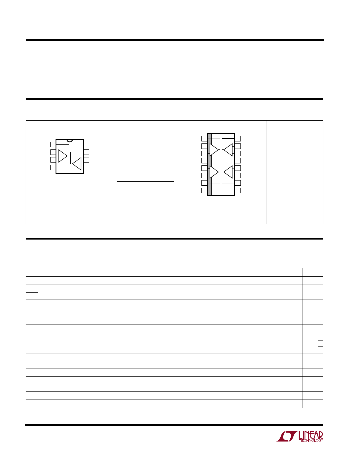
Dual in 8-Pin PDIP and SO Package
■
Quad in a Narrow 16-Pin SO Package
LT1492/LT1493
5MHz, 3V/µs, Low Power
Single Supply, Dual and Quad
Precision Op Amps
U
DESCRIPTION
The LT®1492/LT1493 are dual/quad, low power, single supply precision op amps with 5MHz gain-bandwidth product,
3V/µs slew rate and only 450µ A of quiescent supply current
per amplifier.
With a maximum input offset voltage of only 180µV, the
LT1492/LT1493 eliminate trims in most systems while providing high frequency performance not usually found in low
power single supply amplifiers.
The LT1492/LT1493 will operate on any supply greater than
2.5V and less than 36V total, and are specified on single 3.3V,
single 5V and ±15V supplies. Even with their low quiescent
supply current the minimum output drive is 20mA, ideal for
driving low impedance loads.
The inputs can be driven beyond the supplies without
damage or phase reversal of the output. The low operating
voltage and wide input and output range make the LT1492/
LT1493 amplifiers ideal for battery-powered applications.
U
APPLICATIONS
■
Battery-Powered Systems
Portable Instrumentation
■
Active Filters
■
Photodiode Amplifiers
■
DAC Current to Voltage Amplifiers
TYPICAL APPLICATION
Precision AC to DC Converter (Full Wave Rectifier and Filter)
4.99k
5V
10k
V
IN
–
1/2 LT1492
+
15k
U
+
1/2 LT1492
–
10k
6.49k
VS = 5V, 0V
< 1% ERROR FROM 100mV TO 1V, f = 1kHz
10% ERROR AT 10mV, f = 1kHz
1% ERROR AT 5kHz, V
10% ERROR AT 30kHz, V
10k
+
= 100mV
IN
For applications requiring faster precision single supply
amplifiers, see the 14MHz, 7V/µs LT1211/LT1212, the
28MHz, 12V/µs LT1213/LT1214 or the 23MHz, 50V/µs
LT1215/LT1216.
, LTC and LT are registered trademarks of Linear Technology Corporation.
Distribution of Offset Voltage
Drift with Temperature
50
VS = 5V, 0V
LT1492 N8, S8 PACKAGES
LT1493 S16 PACKAGE
40
30
DC
V
10µF
= 100mV
IN
OUT
RMS
RMS
1492/93 TA01
20
PERCENT OF UNITS (%)
10
0
–1.5
–1
–2 2
–2.5
OFFSET VOLTAGE DRIFT WITH TEMPERATURE (µV/°C)
–0.5
0.5
1
0
1.5
2.5
1492/93 G02
1
LT1492/LT1493
1
2
3
4
5
6
7
8
TOP VIEW
S PACKAGE
16-LEAD PLASTIC SO
16
15
14
13
12
11
10
9
OUT A
–IN A
+IN A
V
+
+IN B
–IN B
OUT B
NC
OUT D
–IN D
+IN D
V
–
+IN C
–IN C
OUT C
NC
C
A
D
B
WW
W
U
ABSOLUTE MAXIMUM RATINGS
Total Supply Voltage (V+ to V–) .............................. 36V
Input Current ...................................................... ±15mA
Output Short-Circuit Duration (Note 1) .........Continuous
Operating Temperature Range ................ –40°C to 85°C
U
W
U
PACKAGE/ORDER INFORMATION
ORDER PART
TOP VIEW
OUT A
1
–IN A
2
+IN A
A
3
–
V
4
N8 PACKAGE
8-LEAD PDIP
S8 PACKAGE
8-LEAD PLASTIC SO
T
= 150°C, θJA = 130°C/ W (N8)
JMAX
T
= 150°C, θJA = 190°C/ W (S8)
JMAX
V+
8
OUT B
7
–IN B
6
B
+IN B
5
NUMBER
LT1492CN8
LT1492CS8
S8 PART MARKING
1492
Specified Temperature Range (Note 2) .....
–40°C to 85°C
Junction Temperature........................................... 150°C
Storage Temperature Range ................. –65°C to 150°C
Lead Temperature (Soldering, 10 sec).................. 300°C
ORDER PART
NUMBER
LT1493CS
T
= 150°C, θJA = 150°C/ W
JMAX
Consult factory for Industrial and Military grade parts.
5V ELECTRICAL CHARACTERISTICS
VS = 5V, 0V; VCM = 0.5V, V
SYMBOL PARAMETER CONDITIONS MIN TYP MAX UNITS
V
OS
∆V
OS
∆Time
I
OS
I
B
e
n
i
n
CMRR Common Mode Rejection Ratio VCM = 0V to 3.4V 86 102 dB
PSRR Power Supply Rejection Ratio VS = 2.5V to 12.5V 90 110 dB
2
Input Offset Voltage 100 180 µV
Long-Term Input Offset Voltage Stability 0.6 µV/Mo
Input Offset Current 520 nA
Input Bias Current 50 100 nA
Input Noise Voltage 0.1Hz to 10Hz 330 nV
Input Noise Voltage Density fO = 10Hz 17.3 nV/√Hz
Input Noise Current Density fO = 10Hz 0.78 pA/√Hz
Input Resistance (Note 3) Differential Mode 10 40 MΩ
Input Capacitance f = 1MHz 10 pF
Input Voltage Range 3.4 3.60 V
= 0.5V, TA = 25°C, unless otherwise noted.
OUT
= 1000Hz 16.5 nV/√Hz
f
O
= 1000Hz 0.14 pA/√Hz
f
O
Common Mode 800 MΩ
0 –0.25 V
P-P
5V ELECTRICAL CHARACTERISTICS
LT1492/LT1493
VS = 5V, 0V; VCM = 0.5V, V
SYMBOL PARAMETER CONDITIONS MIN TYP MAX UNITS
A
VOL
I
O
SR Slew Rate AV = –2 1.8 V/µs
GBW Gain-Bandwidth Product f = 100kHz 4.5 MHz
I
S
tr, t
f
OS Overshoot AV = 1, VO = 100mV 20 %
t
PD
t
S
THD Total Harmonic Distortion AV = 1, VO = 1V
Large-Signal Voltage Gain VO = 0.05V to 3.7V, RL = 2k 175 350 V/mV
Maximum Output Voltage Swing Output High, No Load 4.2 4.35 V
(Note 4) Output High, I
Maximum Output Current (Note 8) ±20 ±60 mA
Supply Current per Amplifier 425 550 µA
Minimum Supply Voltage 2.1 2.5 V
Full Power Bandwidth AV = 1, VO = 2.5V
Rise Time, Fall Time AV = 1, 10% to 90%, VO = 100mV 100 ns
Propagation Delay AV = 1, VO = 100mV 100 ns
Settling Time 0.01%, AV = 1, ∆VO = 2V 2.6 µs
Open-Loop Output Resistance IO = 0mA, f = 2MHz 130 Ω
= 0.5V, TA = 25°C, unless otherwise noted.
OUT
Output High, I
Output Low, No Load 0.003 0.006 V
Output Low, I
Output Low, I
= 1mA 4.1 4.25 V
SOURCE
= 15mA 3.0 3.15 V
SOURCE
= 1mA 0.062 0.075 V
SINK
= 15mA 0.362 0.500 V
SINK
P-P
, f = 20Hz to 20kHz 0.005 %
RMS
150 kHz
VS = 5V, 0V; VCM = 0.5V, V
SYMBOL PARAMETER CONDITIONS MIN TYP MAX UNITS
V
OS
V
OS
∆T
I
OS
I
B
CMRR Common Mode Rejection Ratio VCM = 0V to 3.4V ● 84 102 dB
PSRR Power Supply Rejection Ratio VS = 2.5V to 12.5V ● 90 110 dB
A
VOL
I
S
Input Offset Voltage ● 120 280 µV
Input Offset Voltage Drift (Note 3) ● 13µV/°C
Input Offset Current ● 525 nA
Input Bias Current ● 55 110 nA
Input Voltage Range ● 3.4 3.55 V
Large-Signal Voltage Gain VO = 0.05V to 3.7V, RL = 2k ● 140 250 V/mV
Maximum Output Voltage Swing Output High, No Load ● 4.1 4.25 V
(Note 4) Output High, I
Supply Current per Amplifier ● 470 650 µA
= 0.5V, 0°C ≤ TA ≤ 70°C, unless otherwise noted.
OUT
Output High, I
Output Low, No Load ● 0.004 0.007 V
Output Low, I
Output Low, I
SOURCE
SOURCE
= 1mA ● 0.070 0.085 V
SINK
= 15mA ● 0.390 0.525 V
SINK
● 0 –0.15 V
= 1mA ● 4.0 4.15 V
= 15mA ● 2.9 3.05 V
3
LT1492/LT1493
5V ELECTRICAL CHARACTERISTICS
VS = 5V, 0V; VCM = 0.5V, V
SYMBOL PARAMETER CONDITIONS MIN TYP MAX UNITS
V
OS
V
OS
∆T
I
OS
I
B
CMRR Common Mode Rejection Ratio VCM = 0V to 3.4V ● 80 90 dB
PSRR Power Supply Rejection Ratio VS = 2.5V to 12.5V ● 90 110 dB
A
VOL
I
S
Input Offset Voltage ● 150 325 µV
Input Offset Voltage Drift (Note 3) ● 13µV/°C
Input Offset Current ● 540 nA
Input Bias Current ● 55 130 nA
Input Voltage Range ● 3.4 3.5 V
Large-Signal Voltage Gain VO = 0.05V to 3.7V, RL = 2k ● 140 220 V/mV
Maximum Output Voltage Swing Output High, No Load ● 3.95 4.15 V
(Note 4) Output High, I
Supply Current per Amplifier ● 480 700 µA
= 0.5V, –40°C ≤ TA ≤ 85°C, unless otherwise noted. (Note 2)
OUT
= 1mA ● 3.85 4.05 V
SOURCE
Output High, I
Output Low, No Load ● 0.005 0.008 V
Output Low, I
Output Low, I
= 15mA ● 2.75 2.95 V
SOURCE
= 1mA ● 0.073 0.095 V
SINK
= 15mA ● 0.400 0.575 V
SINK
● 0 – 0.1 V
±15V ELECTRICAL CHARACTERISTICS
VS = ±15V, VCM = 0V, V
SYMBOL PARAMETER CONDITIONS MIN TYP MAX UNITS
V
OS
I
OS
I
B
CMRR Common Mode Rejection Ratio VCM = –15V to 13.4V 86 102 dB
PSRR Power Supply Rejection Ratio VS = ±2V to ±16V 90 113 dB
A
VOL
I
O
SR Slew Rate AV = –2, (Note 5) 2 3 V/µs
GBW Gain-Bandwidth Product f = 100kHz 3 5 MHz
I
S
t
S
Input Offset Voltage 120 450 µV
Input Offset Current 520 nA
Input Bias Current 45 100 nA
Input Voltage Range 13.4 13.6 V
Large-Signal Voltage Gain VO = ±10V, RL = 5k 1500 6500 V/mV
Maximum Output Voltage Swing Output High, I
Maximum Output Current (Note 8) ±20 ±55 mA
Supply Current per Amplifier 500 800 µA
Channel Separation VO = ±10V, RL = 5k 128 140 dB
Minimum Supply Voltage ±1.4 ±2V
Full Power Bandwidth AV = 1, VO = 20V
Settling Time 0.01%, AV = 1, ∆VO = 10V 5.8 µs
= 0V, TA = 25°C, unless otherwise noted.
OUT
Output Low, I
–15.0 –15.2 V
= 15mA 12.9 13.15 V
SOURCE
= 15mA –14.4 –14.6 V
SINK
P-P
30 kHz
4
±15V ELECTRICAL CHARACTERISTICS
LT1492/LT1493
VS = ±15V, VCM = 0V, V
SYMBOL PARAMETER CONDITIONS MIN TYP MAX UNITS
V
OS
V
OS
∆T
I
OS
I
B
CMRR Common Mode Rejection Ratio VCM = –15V to 13.4V ● 84 101 dB
PSRR Power Supply Rejection Ratio VS = ±2V to ±16V ● 90 108 dB
A
VOL
I
S
Input Offset Voltage ● 160 550 µV
Input Offset Voltage Drift (Note 3) ● 13µV/°C
Input Offset Current ● 10 30 nA
Input Bias Current ● 55 120 nA
Input Voltage Range ● 13.4 13.5 V
Large-Signal Voltage Gain VO = ±10V, RL = 5k ● 1200 4000 V/mV
Maximum Output Voltage Swing Output High, I
Supply Current per Amplifier ● 600 930 µA
VS = ±15V, VCM = 0V, V
SYMBOL PARAMETER CONDITIONS MIN TYP MAX UNITS
V
OS
V
OS
∆T
I
OS
I
B
CMRR Common Mode Rejection Ratio VCM = –15V to 13.4V ● 82 101 dB
PSRR Power Supply Rejection Ratio VS = ±2V to ±16V ● 90 108 dB
A
VOL
I
S
Input Offset Voltage ● 180 650 µV
Input Offset Voltage Drift (Note 3) ● 13µV/°C
Input Offset Current ● 10 50 nA
Input Bias Current ● 55 150 nA
Input Voltage Range ● 13.4 13.45 V
Large-Signal Voltage Gain VO = ±10V, RL = 5k ● 1000 3500 V/mV
Maximum Output Voltage Swing Output High, I
Supply Current per Amplifier ● 620 1000 µA
= 0V, 0°C ≤ TA ≤ 70°C, unless otherwise noted.
OUT
= 15mA ● 12.7 13.0 V
SOURCE
Output Low, I
= 0V, –40°C ≤ TA ≤ 85°C, unless otherwise noted. (Note 2)
OUT
Output Low, I
= 15mA ● –14.2 –14.6 V
SINK
= 15mA ● 12.5 12.9 V
SOURCE
= 15mA ● –14.1 –14.6 V
SINK
● –15.0 –15.1 V
● –15.0 –15.05 V
5
 Loading...