

Linear Technology LT1468 Datasheet

FEATURES
LT1468
90MHz, 22V/µs
16-Bit Accurate
Operational Amplifier
U
DESCRIPTIO
■
90MHz Gain Bandwidth, f = 100kHz
■
22V/µs Slew Rate
■
Settling Time: 900ns (AV = –1, 150µV, 10V Step)
■
Low Distortion, –96.5dB for 100kHz, 10V
■
Maximum Input Offset Voltage: 75µV
■
Maximum Input Offset Voltage Drift: 2µV/°C
■
Maximum (–) Input Bias Current: 10nA
■
Minimum DC Gain: 1000V/mV
■
Minimum Output Swing into 2k: ±12.8V
■
Unity Gain Stable
■
Input Noise Voltage: 5nV/√Hz
■
Input Noise Current: 0.6pA/√Hz
■
Total Input Noise Optimized for 1k < RS < 20k
■
Specified at ±5V and ±15V
P-P
U
APPLICATIONS
■
16-Bit DAC Current-to-Voltage Converter
■
Precision Instrumentation
■
ADC Buffer
■
Low Distortion Active Filters
■
High Accuracy Data Acquisition Systems
■
Photodiode Amplifiers
The LT®1468 is a precision high speed operational amplifier with 16-bit accuracy and 900ns settling to 150µV for
10V signals. This unique blend of precision and AC performance makes the LT1468 the optimum choice for high
accuracy applications such as DAC current-to-voltage
conversion and ADC buffers. The initial accuracy and drift
characteristics of the input offset voltage and inverting
input bias current are tailored for inverting applications.
The 90MHz gain bandwidth ensures high open-loop gain
at frequency for reducing distortion. In noninverting applications such as an ADC buffer, the low distortion and DC
accuracy allow full 16-bit AC and DC performance.
The 22V/µ s slew rate of the LT1468 improves large-signal
performance in applications such as active filters and
instrumentation amplifiers compared to other precision
op amps.
The LT1468 is manufactured on Linear Technology’s
complementary bipolar process.
, LTC and LT are registered trademarks of Linear Technology Corporation.
U
TYPICAL APPLICATIO
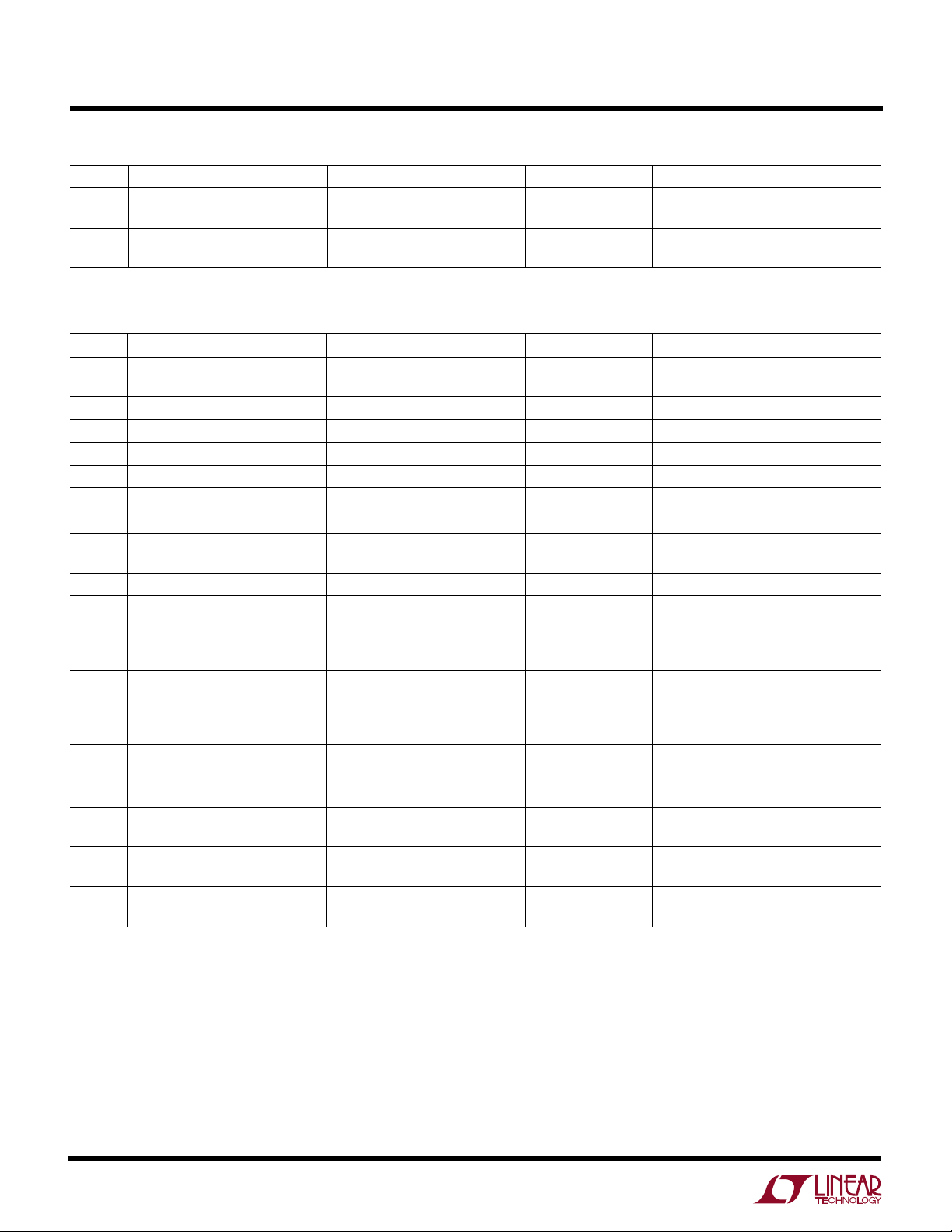
16-Bit DAC I-to-V Converter
20pF
16
DAC
INPUTS
LTC
OFFSET: VOS + IB (6kΩ) < 1LSB
SETTLING TIME TO 150µV = 1.7µs
SETTLING LIMITED BY 6k AND 20pF TO COMPENSATE DAC OUTPUT CAPACITANCE
®
1597
6k
–
+
LT1468
2k
V
OUT
50pF
OPTIONAL NOISE FILTER
1468 TA01
Total Harmonic Distortion vs Frequency
–80
VS = ±15V
= 2
A
V
= 2k
R
L
–90
–100
–110
–120
TOTAL HARMONIC DISTORTION (dB)
–130
100
= 10V
V
OUT
P-P
1k 10k 100k
FREQUENCY (Hz)
1468 TA02
1
LT1468
1
2
3
4
8
7
6
5
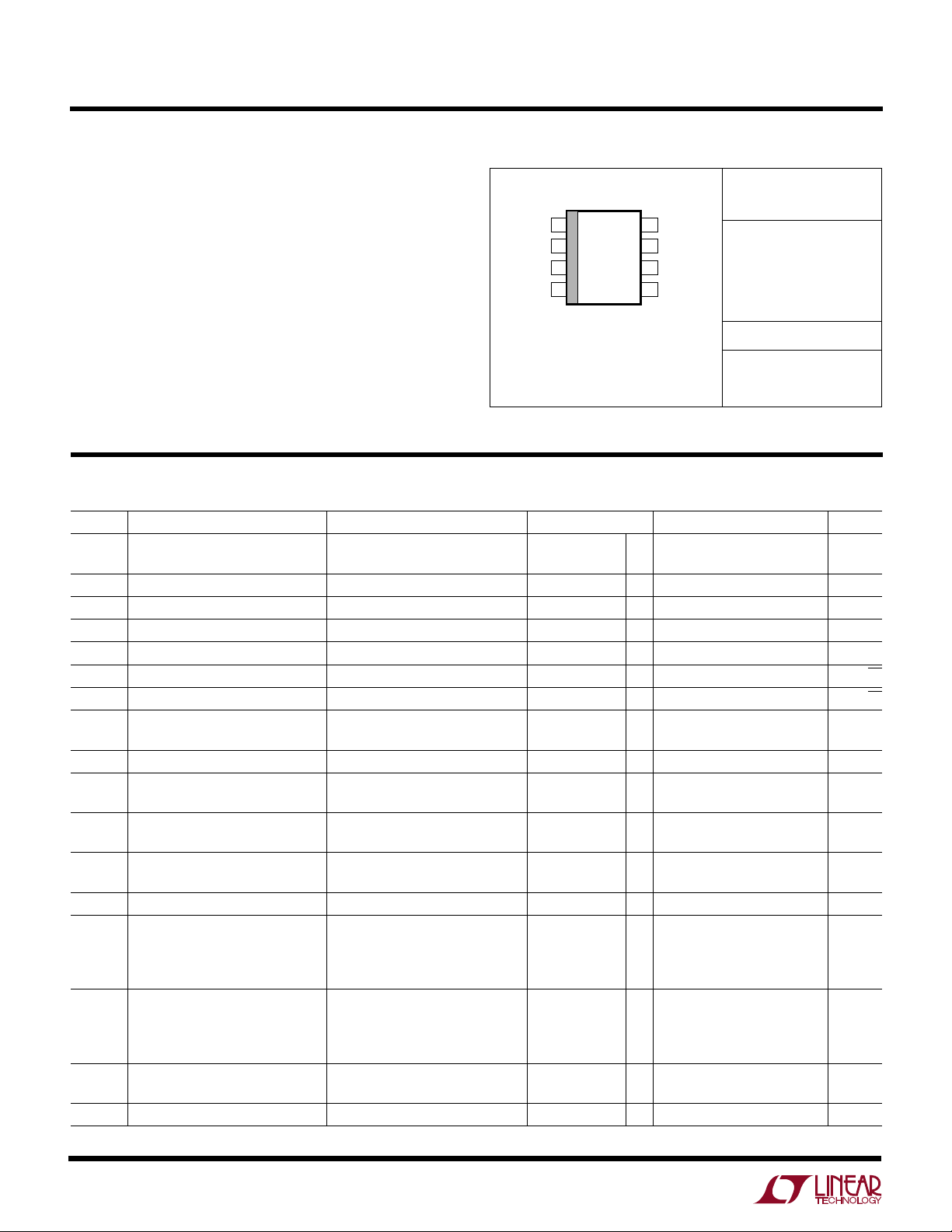
TOP VIEW
*DO NOT CONNECT
S8 PACKAGE
8-LEAD PLASTIC SO
N8 PACKAGE
8-LEAD PDIP
NULL
–IN
+IN
V
–
DNC*
V
+
V
OUT
NULL
WW
W
ABSOLUTE AXI U RATI GS
(Note 1)
Total Supply Voltage (V+ to V–) ............................... 36V
U
UUW
PACKAGE/ORDER I FOR ATIO
ORDER PART
NUMBER
Maximum Input Current (Note 2) ......................... 10mA
Output Short-Circuit Duration (Note 3)............ Indefinite
Operating Temperature Range ................ –40°C to 85°C
Specified Temperature Range (Note 4)... –40°C to 85°C
Junction Temperature...........................................150°C
Storage Temperature Range ................. –65°C to 150°C
Lead Temperature (Soldering, 10 sec)..................300°C
T
= 150°C, θJA = 130°C/W (N8)
JMAX
= 150°C, θJA = 190°C/W (S8)
T
JMAX
LT1468CN8
LT1468CS8
LT1468IN8
LT1468IS8
S8 PART MARKING
1468
1468I
Consult factory for Military Grade parts.
ELECTRICAL CHARACTERISTICS
SYMBOL PARAMETER CONDITIONS V
V
OS
I
OS
–
I
B
+
I
B
e
n
i
n
R
IN
C
IN
CMRR Common Mode Rejection Ratio V
PSRR Power Supply Rejection Ratio VS = ±4.5V to ±15V 100 112 dB
A
VOL
V
OUT
I
OUT
I
SC
Input Offset Voltage ±15V 30 75 µV
Input Offset Current ±5V to ±15V 13 50 nA
Inverting Input Bias Current ±5V to ±15V 3 ±10 nA
Noninverting Input Bias Current ±5V to ±15V –10 ±40 nA
Input Noise Voltage 0.1Hz to 10Hz ±5V to ±15V 0.3 µV
Input Noise Voltage f = 10kHz ±5V to ±15V 5 nV/√Hz
Input Noise Current f = 10kHz ±5V to ±15V 0.6 pA/√Hz
Input Resistance V
Input Capacitance ±15V 4 pF
Input Voltage Range + ±15V 12.5 13.5 V
Input Voltage Range – ±15V –14.3 –12.5 V
Large-Signal Voltage Gain V
Output Swing RL = 10k, V
Output Current V
Short-Circuit Current V
= ±12.5V ±15V 100 240 MΩ
CM
Differential ±15V 50 150 kΩ
= ±12.5V ±15V 96 110 dB
CM
= ±2.5V ±5V 96 112 dB
V
CM
= ±12.5V, RL = 10k ±15V 1000 9000 V/mV
OUT
V
= ±12.5V, RL = 2k ±15V 500 5000 V/mV
OUT
= ±2.5V, RL = 10k ±5V 1000 6000 V/mV
V
OUT
= ±2.5V, RL = 2k ±5V 500 3000 V/mV
V
OUT
= 2k, V
R
L
R
= 10k, V
L
= 2k, V
R
L
= ±12.5V ±15V ±15 ±22 mA
OUT
= ±2.5V ±5V ±15 ±22 mA
V
OUT
= 0V, V
OUT
TA = 25°C, VCM = 0V unless otherwise noted.
SUPPLY
±5V 50 175 µV
±5V 2.5 3.5 V
±5V –4.3 –2.5 V
= ±1mV ±15V ±13.0 ±13.6 V
IN
= ±1mV ±15V ±12.8 ±13.5 V
IN
= ±1mV ±5V ±3.0 ±3.6 V
IN
= ±1mV ±5V ±2.8 ±3.5 V
IN
= ±0.2V ±15V ±25 ±40 mA
IN
MIN TYP MAX UNITS
P-P
2
LT1468
ELECTRICAL CHARACTERISTICS
SYMBOL PARAMETER CONDITIONS V
TA = 25°C, VCM = 0V unless otherwise noted.
SUPPLY
MIN TYP MAX UNITS
SR Slew Rate AV = –1, RL = 2k (Note 5) ±15V 15 22 V/µs
±5V 11 17 V/µs
Full-Power Bandwidth 10V Peak, (Note 6) ±15V 350 kHz
3V Peak, (Note 6) ±5V 900 kHz
GBW Gain Bandwidth f = 100kHz, RL = 2k ±15V 60 90 MHz
±5V 55 88 MHz
THD Total Harmonic Distortion AV = 2, VO = 10V
= 2, VO = 10V
A
V
tr, t
f
Rise Time, Fall Time AV = 1, 10% to 90%, 0.1V ±15V 11 ns
, f = 1kHz ±15V 0.00007 %
P-P
, f = 100kHz ±15V 0.0015 %
P-P
±5V 12 ns
Overshoot AV = 1, 0.1V ±15V 30 %
±5V 35 %
Propagation Delay AV = 1, 50% VIN to 50% V
, 0.1V ±15V 9 ns
OUT
±5V 10 ns
t
s
R
O
I
S
Settling Time 10V Step, 0.01%, AV = –1 ±15V 760 ns
10V Step, 150µV, A
5V Step, 0.01%, A
= –1 ±15V 900 ns
V
= –1 ±5V 770 ns
V
Output Resistance AV = 1, f = 100kHz ±15V 0.02 Ω
Supply Current ±15V 3.9 5.2 mA
±5V 3.6 5.0 mA
0°C ≤ TA ≤ 70°C, VCM = 0V unless otherwise noted.
SYMBOL PARAMETER CONDITIONS V
V
OS
Input Offset Voltage ±15V ● 150 µV
SUPPLY
±5V
Input VOS Drift (Note 7) ±5V to ±15V ● 0.7 2.0 µV/°C
I
OS
Input Offset Current ±5V to ±15V ● 65 nA
Input Offset Current Drift ±5V to ±15V 60 pA/°C
–
I
B
Inverting Input Bias Current ±5V to ±15V ● ±15 nA
Negative Input Current Drift ±5V to ±15V 40 pA/°C
+
I
B
CMRR Common Mode Rejection Ratio V
Noninverting Input Bias Current ±5V to ±15V ● ±50 nA
= ±12.5V ±15V ● 94 dB
CM
= ±2.5V ±5V ● 94 dB
V
CM
PSRR Power Supply Rejection Ratio VS = ±4.5V to ±15V ● 98 dB
A
V
I
I
VOL
OUT
OUT
SC
Large-Signal Voltage Gain V
= ±12.5V, RL = 10k ±15V ● 500 V/mV
OUT
= ±12.5V, RL = 2k ±15V ● 250 V/mV
V
OUT
V
= ±2.5V, RL = 10k ±5V ● 500 V/mV
OUT
= ±2.5V, RL = 2k ±5V ● 250 V/mV
V
OUT
Output Swing RL = 10k, V
= 2k, V
R
L
= 10k, V
R
L
R
= 2k, V
L
Output Current V
Short-Circuit Current V
= ±12.5V ±15V ● ±12.5 mA
OUT
= ±2.5V ±5V ● ±12.5 mA
V
OUT
= 0V, V
OUT
= ±1mV ±15V ● ±12.9 V
IN
= ±1mV ±15V ● ±12.7 V
IN
= ±1mV ±5V ● ±2.9 V
IN
= ±1mV ±5V ● ±2.7 V
IN
= ±0.2V ±15V ● ±17 mA
IN
SR Slew Rate AV = –1, RL = 2k (Note 5) ±15V ● 13 V/µs
±5V
MIN TYP MAX UNITS
● 250 µV
● 9V/µs
3
LT1468
ELECTRICAL CHARACTERISTICS
SYMBOL PARAMETER CONDITIONS V
0°C ≤ TA ≤ 70°C, VCM = 0V unless otherwise noted.
SUPPLY
MIN TYP MAX UNITS
GBW Gain Bandwidth f = 100kHz, RL = 2k ±15V ● 55 MHz
±5V
I
S
Supply Current ±15V ● 6.5 mA
±5V
● 50 MHz
● 6.3 mA
–40°C ≤ TA ≤ 85°C, VCM = 0V unless otherwise noted (Note 4).
SYMBOL PARAMETER CONDITIONS V
V
OS
Input Offset Voltage ±15V ● 230 µV
SUPPLY
±5V
Input VOS Drift (Note 7) ±5V to ±15V ● 0.7 2.5 µV/°C
I
OS
Input Offset Current ±5V to ±15V ● 80 nA
Input Offset Current Drift ±5V to ±15V 120 pA/°C
–
I
B
Inverting Input Bias Current ±5V to ±15V ● ±30 nA
Negative Input Current Drift ±5V to ±15V 80 pA/°C
+
I
B
CMRR Common Mode Rejection Ratio V
Noninverting Input Bias Current ±5V to ±15V ● ±60 nA
= ±12.5V ±15V ● 92 dB
CM
= ±2.5V ±5V ● 92 dB
V
CM
PSRR Power Supply Rejection Ratio VS = ±4.5V to ±15V ● 96 dB
A
VOL
V
OUT
I
OUT
I
SC
Large-Signal Voltage Gain V
= ±12V, RL = 10k ±15V ● 300 V/mV
OUT
= ±10V, RL = 2k ±15V ● 150 V/mV
V
OUT
V
= ±2.5V, RL = 10k ±5V ● 300 V/mV
OUT
= ±2.5V, RL = 2k ±5V ● 150 V/mV
V
OUT
Output Swing RL = 10k, V
= 2k, V
R
L
R
= 10k, V
L
= 2k, V
R
L
Output Current V
Short-Circuit Current V
= ±12.5V ±15V ● ±7mA
OUT
= ±2.5V ±5V ● ±7mA
V
OUT
= 0V, V
OUT
= ±1mV ±15V ● ±12.8 V
IN
= ±1mV ±15V ● ±12.6 V
IN
= ±1mV ±5V ● ±2.8 V
IN
= ±1mV ±5V ● ±2.6 V
IN
= ±0.2V ±15V ● ±12 mA
IN
SR Slew Rate AV = –1, RL = 2k (Note 5) ±15V ● 9V/µs
±5V
GBW Gain Bandwidth f = 100kHz, RL = 2k ±15V ● 45 MHz
±5V
I
S
Supply Current ±15V ● 7.0 mA
±5V
MIN TYP MAX UNITS
● 330 µV
● 6V/µs
● 40 MHz
● 6.8 mA
The ● denotes specifications that apply over the full operating
temperature range.
Note 1: Absolute Maximum Ratings are those values beyond which the life
of a device may be impaired.
Note 2: The inputs are protected by back-to-back diodes and two 100Ω
series resistors. If the differential input voltage exceeds 0.7V, the input
current should be limited to 10mA. Input voltages outside the supplies will
be clamped by ESD protection devices and input currents should also be
limited to 10mA.
Note 3: A heat sink may be required to keep the junction temperature
below absolute maximum when the output is shorted indefinitely.
4
Note 4: The LT1468C is guaranteed to meet specified performance from
0°C to 70°C and is designed, characterized and expected to meet these
extended temperature limits, but is not tested at –40°C and at 85°C. The
LT1468I is guaranteed to meet the extended temperature limits.
Note 5: Slew rate is measured between ±8V on the output with ±12V input
for ±15V supplies and ±2V on the output with ±3V input for ±5V supplies.
Note 6: Full power bandwidth is calculated from the slew rate
measurement: FPBW = SR/2πV
P
Note 7: This parameter is not 100% tested.
 Loading...