

FEATURES
■
Trimmed to High Accuracy: 0.04% Max
■
Low Drift: 3ppm/°C Max
■
Low Supply Current: 50µA Max
■
Temperature Coefficient Guaranteed to 125°C
■
High Output Current: 50mA Min
■
Low Dropout Voltage: 300mV Max
■
Excellent Thermal Regulation
■
Power Shutdown
■
Thermal Limiting
■
Operating Temperature Range: –40°C to 125°C
■
Voltage Options: 2.5V, 3V, 3.3V, 4.096V and 5V
U
APPLICATIO S
■
A/D and D/A Converters
■
Precision Regulators
■
Handheld Instruments
■
Power Supplies
LT1461
Micropower Precision
Low Dropout Series
Voltage Reference Family
U
DESCRIPTIO
The LT®1461 is a family of low dropout micropower bandgap
references that combine very high accuracy and low drift with
low supply current and high output drive. These series
references use advanced curvature compensation techniques
to obtain low temperature coefficient and trimmed precision
thin-film resistors to achieve high output accuracy. The
LT1461 family draws only 35µA of supply current, making
them ideal for low power and portable applications, however
their high 50mA output drive makes them suitable for higher
power requirements, such as precision regulators.
In low power applications, a dropout voltage of less than
300mV ensures maximum battery life while maintaining full
reference performance. Line regulation is nearly immeasurable, while the exceedingly good load and thermal regulation
will not add significantly to system error budgets. The
shutdown feature can be used to switch full load currents and
can be used for system power down. Thermal shutdown
protects the part from overload conditions. The LT1461 is
available in 2.5V, 3V, 3.3V 4.096V and 5V options.
, LTC and LT are registered trademarks of Linear Technology Corporation.
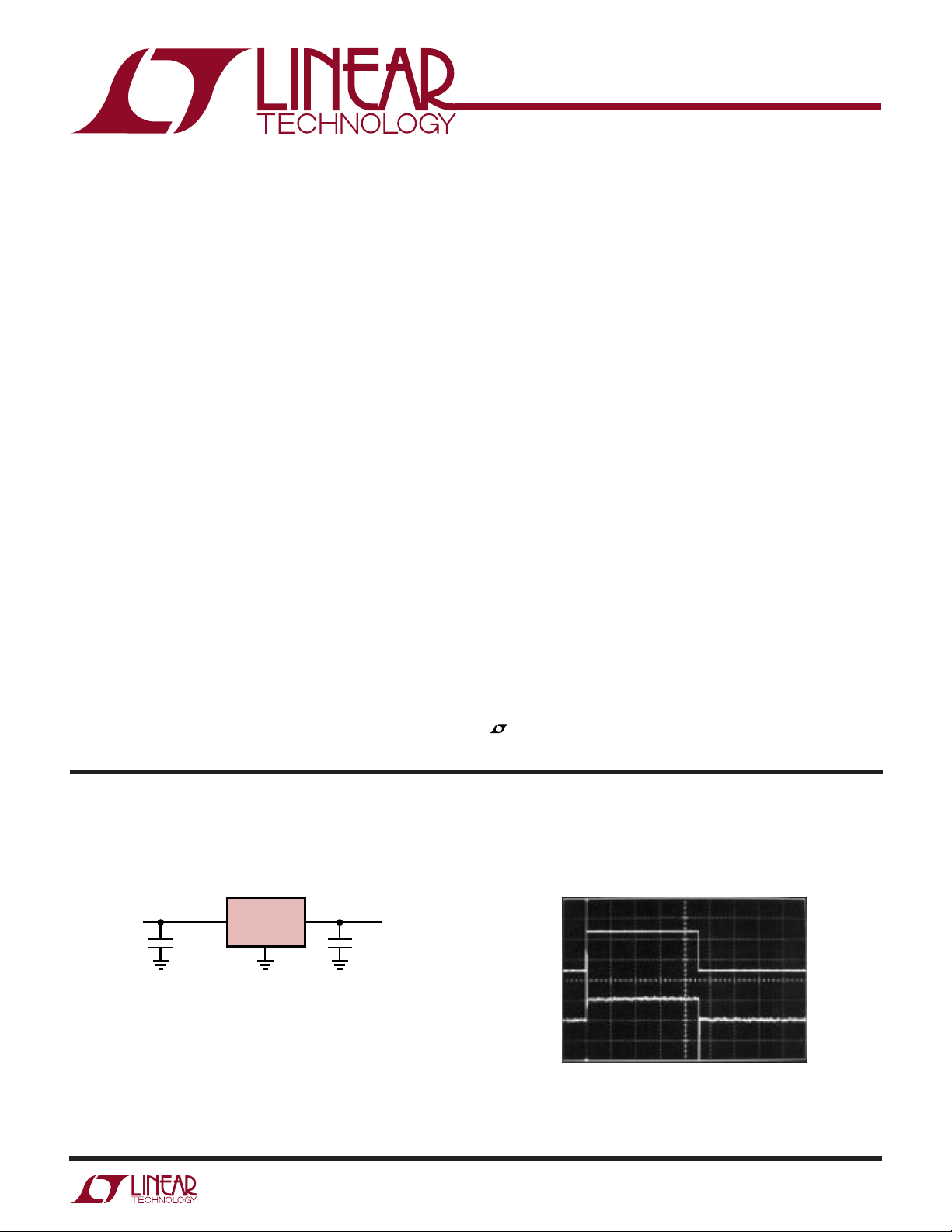
TYPICAL APPLICATIO
Basic Connection
(V
+ 0.3V) ≤ VIN ≤ 20V
OUT
C
1µF
IN
LT1461
U
C
L
2µF
1461 TA01
LT1461-2.5 Load Regulation, P
V
OUT
V
OUT
0mA
I
OUT
20mA
LOAD REG
1mV/DIV
10ms/DIV
= 200mW
DISS
1461 TA02
1
LT1461
WWWU
ABSOLUTE AXI U RATI GS
(Note 1)
Input Voltage ........................................................... 20V
Output Short-Circuit Duration......................... Indefinite
Operating Temperature Range
(Note 2) ........................................... –40°C to 125°C
Storage Temperature Range (Note 3) ... –65°C to 150°C
UU
W
PACKAGE/ORDER I FOR ATIO
ORDER PART
NUMBER
TOP VIEW
DNC*
1
V
2
IN
SHDN
3
GND
4
S8 PACKAGE
8-LEAD PLASTIC SO
*DNC: DO NOT CONNECT
T
= 150°C, θJA = 190°C/W
JMAX
(Note 3)
LT1461ACS8-2.5
LT1461BCS8-2.5
8
DNC*
LT1461CCS8-2.5
DNC*
7
6
5
LT1461AIS8-2.5
V
OUT
LT1461BIS8-2.5
DNC*
LT1461CIS8-2.5
LT1461DHS8-2.5
LT1461ACS8-3
LT1461BCS8-3
LT1461CCS8-3
LT1461AIS8-3
LT1461BIS8-3
LT1461CIS8-3
LT1461DHS8-3
LT1461ACS8-3.3
LT1461BCS8-3.3
LT1461CCS8-3.3
LT1461AIS8-3.3
LT1461BIS8-3.3
LT1461CIS8-3.3
LT1461DHS8-3.3
LT1461ACS8-4
LT1461BCS8-4
LT1461CCS8-4
LT1461AIS8-4
LT1461BIS8-4
LT1461CIS8-4
LT1461DHS8-4
Specified Temperature Range
Commercial ............................................ 0°C to 70°C
Industrial ........................................... –40°C to 85°C
High................................................. – 40°C to 125°C
Lead Temperature (Soldering, 10 sec)..................300°C
S8 PART MARKING
LT1461ACS8-5
LT1461BCS8-5
LT1461CCS8-5
LT1461AIS8-5
LT1461BIS8-5
LT1461CIS8-5
LT1461DHS8-5
461A25
461B25
461C25
61AI25
61BI25
61CI25
61DH25
1461A3
1461B3
1461C3
461AI3
461BI3
461CI3
461DH3
461A33
461B33
461C33
61AI33
61BI33
61CI33
61DH33
1461A4
1461B4
1461C4
461AI4
461BI4
461CI4
461DH4
1461A5
1461B5
1461C5
461AI5
461BI5
461CI5
461DH5
Consult factory for Military grade parts.
U
AVAILABLE OPTIO S
INITIAL TEMPERATURE TEMPERATURE
ACCURACY COEFFICIENT RANGE 2.5V 3.0V 3.3V 4.096V 5.0V
0.04% Max 3ppm/°C Max 0°C to 70°C LT1461ACS8-2.5 LT1461ACS8-3 LT1461ACS8-3.3 LT1461ACS8-4 LT1461ACS8-5
0.04% Max 3ppm/°C Max –40°C to 85°C LT1461AIS8-2.5 LT1461AIS8-3 LT1461AIS8-3.3 LT1461AIS8-4 LT1461AIS8-5
0.06% Max 7ppm/°C Max 0°C to 70°C LT1461BCS8-2.5 LT1461BCS8-3 LT1461BCS8-3.3 LT1461BCS8-4 LT1461BCS8-5
0.06% Max 7ppm/°C Max – 40°C to 85°C LT1461BIS8-2.5 LT1461BIS8-3 LT1461BIS8-3.3 LT1461BIS8-4 LT1461BIS8-5
0.08% Max 12ppm/°C Max 0°C to 70°C LT1461CCS8-2.5 LT1461CCS8-3 LT1461CCS8-3.3 LT1461CCS8-4 LT1461CCS8-5
0.08% Max 12ppm/°C Max –40°C to 85°C LT1461CIS8-2.5 LT1461CIS8-3 LT1461CIS8-3.3 LT1461CIS8-4 LT1461CIS8-5
0.15% Max 20ppm/°C Max –40°C to 125°C LT1461DHS8-2.5 LT1461DHS8-3 LT1461DHS8-3.3 LT1461DHS8-4 LT1461DHS8-5
OUTPUT VOLTAGE
2
LT1461
ELECTRICAL CHARACTERISTICS
range, otherwise specifications are at TA = 25°C. VIN – V
The ● denotes specifications which apply over the specified temperature
= 0.5V, Pin 3 = 2.4V, CL = 2µF, unless otherwise specified.
OUT
PARAMETER CONDITIONS MIN TYP MAX UNITS
Output Voltage (Note 4) LT1461ACS8/LT1461AIS8 –0.04 0.04 %
LT1461BCS8/LT1461BIS8 –0.06 0.06 %
LT1461CCS8/LT1461CIS8 –0.08 0.08 %
LT1461DHS8 –0.15 0.15 %
Output Voltage Temperature Coefficient (Note 5) LT1461ACS8/LT1461AIS8 ● 1 3 ppm/°C
● 3 7 ppm/°C
● 5 12 ppm/°C
● 7 20 ppm/°C
● 12 ppm/V
Line Regulation (V
LT1461BCS8/LT1461BIS8
LT1461CCS8/LT1461CIS8
LT1461DHS8
+ 0.5V) ≤ VIN ≤ 20V 2 8 ppm/V
OUT
LT1461DHS8 ● 15 50 ppm/V
Load Regulation Sourcing (Note 6) VIN = V
LT1461DHS8, 0 ≤ I
Dropout Voltage VIN – V
Output Current Short V
+ 2.5V
OUT
0 ≤ I
≤ 50mA 12 30 ppm/mA
OUT
≤ 10mA ● 50 ppm/mA
OUT
, V
OUT
I
= 0mA 0.06 V
OUT
I
= 1mA ● 0.13 0.3 V
OUT
I
= 10mA ● 0.20 0.4 V
OUT
I
= 50mA, I and C Grades Only ● 1.50 2.0 V
OUT
OUT
Error = 0.1%
OUT
to GND 100 mA
● 40 ppm/mA
Shutdown Pin Logic High Input Voltage ● 2.4 V
Logic High Input Current, Pin 3 = 2.4V
● 215 µA
Logic Low Input Voltage ● 0.8 V
Logic Low Input Current, Pin 3 = 0.8V
● 0.5 4 µA
Supply Current No Load 35 50 µA
● 70 µA
Shutdown Current RL = 1k 25 35 µA
● 55 µA
Output Voltage Noise (Note 7) 0.1Hz ≤ f ≤ 10Hz 8 ppm
10Hz ≤ f ≤ 1kHz 9.6 ppm
P-P
RMS
Long-Term Drift of Output Voltage, SO-8 Package (Note 8) See Applications Information 60 ppm/√kHr
Thermal Hysteresis (Note 9) ∆T = 0°C to 70°C 40 ppm
∆T = –40°C to 85°C 75 ppm
∆T = –40°C to 125°C 120 ppm
Note 1: Absolute Maximum Ratings are those values beyond which the life
of a device may be impaired.
Note 2: The LT1461 is guaranteed functional over the operating
temperature range of –40°C to 125°C.
Note 3: If the part is stored outside of the specified temperature range, or
the junction temperature exceeds the specified temperature range, the
output may shift due to hysteresis.
Note 4: ESD (Electrostatic Discharge) sensitive device. Extensive use of
ESD protection devices are used internal to the LT1461, however, high
electrostatic discharge can damage or degrade the device. Use proper ESD
handling precautions.
Note 5: Temperature coefficient is calculated from the minimum and
maximum output voltage measured at T
TC = (V
OMAX
– V
OMIN
)/(T
MAX
– T
MIN
)
, Room and T
MIN
as follows:
MAX
Incremental slope is also measured at 25°C.
Note 6: Load regulation is measured on a pulse basis from no load to the
specified load current. Output changes due to die temperature change
must be taken into account separately.
Note 7: Peak-to-peak noise is measured with a single pole highpass filter
at 0.1Hz and a 2-pole lowpass filter at 10Hz. The unit is enclosed in a stillair environment to eliminate thermocouple effects on the leads. The test
time is 10 seconds. RMS noise is measured with a single pole highpass
filter at 10Hz and a 2-pole lowpass filter at 1kHz. The resulting output is
full-wave rectified and then integrated for a fixed period, making the final
reading an average as opposed to RMS. A correction factor of 1.1 is used
to convert from average to RMS and a second correction of 0.88 is used to
correct for the nonideal bandpass of the filters.
3
LT1461
ELECTRICAL CHARACTERISTICS
Note 8: Long-term drift typically has a logarithmic characteristic and
therefore, changes after 1000 hours tend to be much smaller than before
that time. Total drift in the second thousand hours is normally less than
one third that of the first thousand hours with a continuing trend toward
reduced drift with time. Long-term drift will also be affected by differential
stresses between the IC and the board material created during board
assembly. See the Applications Information section.
Note 9: Hysteresis in output voltage is created by package stress that
depends on whether the IC was previously at a higher or lower
temperature. Output voltage is always measured at 25°C, but the IC is
cycled hot or cold before successive measurements. Hysteresis is roughly
proportional to the square of the temperature change. Hysteresis is not
normally a problem for operational temperature excursions where the
instrument might be stored at high or low temperature. See Applications
Information section.
UW
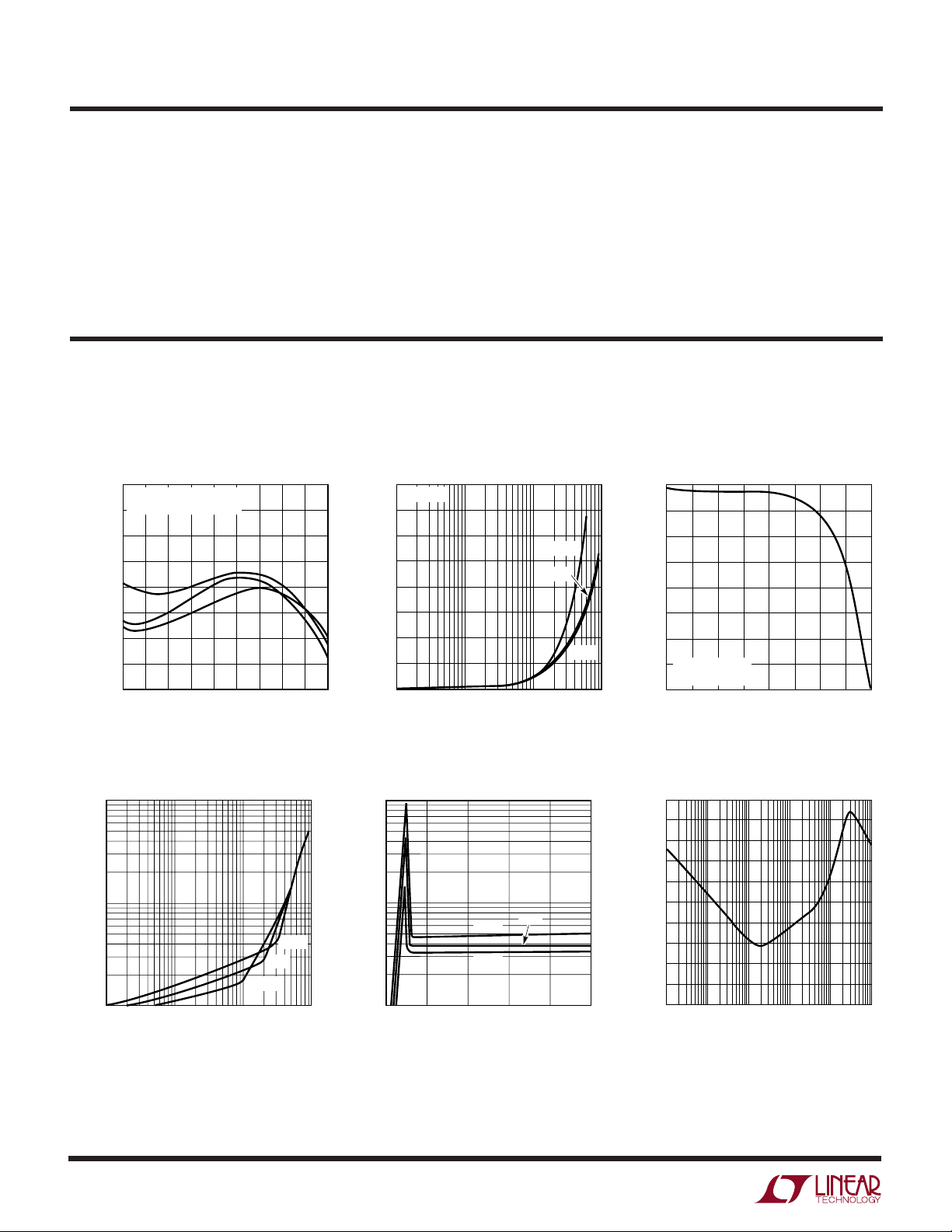
TYPICAL PERFOR A CE CHARACTERISTICS
Curves from the LT1461-2.5 and the LT1461-5 represent the extremes of the voltage options. Characteristic curves for other output
voltages fall between these curves and can be estimated based on their output.
2.5V Reference Voltage
vs Temperature
2.5020
TEMPCO –60°C TO 120°C
3 TYPICAL PARTS
2.5015
2.5010
2.5005
2.5000
2.4995
2.4990
REFERENCE VOLTAGE (V)
2.4985
2.4980
–60 –40 –20
TEMPERATURE (°C)
0 20 40 120
60 80 100
1461 G01
2.5V Load Regulation
1600
VIN = 7.5V
1200
800
400
OUTPUT VOLTAGE CHANGE (ppm)
0
0.1
1 10 100
OUTPUT CURRENT (mA)
Characteristic curves are similar for most LT1461s.
2.5V Line Regulation
vs Temperature
0
–1
125°C
25°C
–55°C
1461 G02
–2
–3
–4
–5
–6
LINE REGULATION (ppm/V)
–7
SUPPLY ∆ = 15V
5V – 20V
–8
–40 –20
20
0
TEMPERATURE (°C)
40
60
100
80
120
1461 G03
2.5V Minimum Input/Output
Voltage Differential vs Load Current
10
1
INPUT/OUTPUT VOLTAGE (V)
–55°C
0.1
0.1
1 10 100
OUTPUT CURRENT (mA)
4
25°C
125°C
1461 G04
2.5V Supply Current
vs Input Voltage
1000
100
SUPPLY CURRENT (µA)
10
5252015100
25°C
125°C
–55°C
INPUT VOLTAGE (V)
1461 G05
2.5V Ripple Rejection Ratio
vs Frequency
100
90
80
70
60
50
40
30
20
RIPPLE REJECTION RATIO (dB)
10
0
0.01
0.1 1 10010 1000
FREQUENCY (kHz)
1641 G06
LT1461
UW
TYPICAL PERFOR A CE CHARACTERISTICS
Curves from the LT1461-2.5 and the LT1461-5 represent the extremes of the voltage options. Characteristic curves for other output
voltages fall between these curves and can be estimated based on their output.
2.5V Output Impedance
vs Frequency 2.5V Turn-On Time
1000
C
= 2µF
OUT
C
= 1µF
100
10
OUTPUT IMPEDANCE (Ω)
1
0.01
0.1 1 10
FREQUENCY (kHz)
OUT
1461 G07
20
10
0
VOLTAGE (V)
2
1
0
V
IN
V
OUT
TIME (100µs/DIV)
Characteristic curves are similar for most LT1461s.
2.5V Turn-On Time
V
IN
V
OUT
TIME (100µs/DIV)
CIN = 1µF
C
= 2µF
L
R
= 50Ω
L
CIN = 1µF
C
= 2µF
L
R
=
∞
L
1461 G08
20
10
0
VOLTAGE (V)
2
1
0
1461 G09
I
OUT
0mA
10mA/DIV
V
OUT
50mV/DIV
2.5V Transient Response to 10mA
Load Step
CL = 2µF
1461 G10
5V
V
IN
4V
V
OUT
50mV/DIV
2.5V Line Transient Response
CIN = 0.1µF
1461 G11
2.5V Output Noise
0.1Hz ≤ f ≤ 10Hz
OUTPUT NOISE (10µV/DIV)
TIME (2SEC/DIV)
1461 G12
5

LT1461
FREQUENCY (kHz)
0.01
40
RIPPLE REJECTION RATIO (dB)
50
60
70
80
0.1 1 10 100 1000
1461 G18
30
20
10
0
90
100
UW
TYPICAL PERFOR A CE CHARACTERISTICS
Curves from the LT1461-2.5 and the LT1461-5 represent the extremes of the voltage options. Characteristic curves for other output
voltages fall between these curves and can be estimated based on their output.
Characteristic curves are similar for most LT1461s.
5V Reference Voltage
vs Temperature
5.0040
TEMPCO –60°C TO 120°C
5.0030
3 TYPICAL PARTS
5.0020
5.0010
5.0000
4.9990
4.9980
4.9970
4.9960
REFERENCE VOLTAGE (V)
4.9950
4.9940
4.9930
–60
–40
–20
20
0
40
TEMPERATURE (°C)
60 80 100
5V Minimum Input/Output Voltage
Differential vs Load Current
10
1
125°C
25°C
0.1
INPUT/OUTPUT VOLTAGE (V)
–55°C
1461 G13
120
5V Load Regulation
2000
VIN = 10V
1600
1200
800
LOAD REGULATION (ppm)
400
0
0.1
OUTPUT CURRENT (mA)
5V Supply Current
vs Input Voltage
10000
1000
100
SUPPLY CURRENT (µA)
10
125°C
25°C
–55°C
25°C
–55°C
1 10 100
125°C
–55°C
125°C
1461 G14
25°C
5V Line Regulation
vs Temperature
0
–1
–2
–3
–4
–5
–6
LINE REGULATION (ppm/V)
–7
SUPPLY ∆ = 14V
6V TO 20V
–8
–40
–20
0
20
TEMPERATURE (
5V Ripple Rejection Ratio
vs Frequency
40
60
80
°C)
100
1461 G15
120
0.01
0.1
5V Output Impedance vs Frequency 5V Turn-On Time
1000
100
10
OUTPUT IMPEDANCE (Ω)
1
0.01
6
1 10 100
OUTPUT CURRENT (mA)
C
C
= 2µF
OUT
0.1 1 10
FREQUENCY (kHz)
OUT
1461 G16
= 1µF
1461 G19
1
0101520
5
2V/DIV
INPUT VOLTAGE (V)
V
6
4
2
0
4
2
0
IN
200µs/DIV
V
OUT
1461 G17
CIN = 1µF
C
= 2µF
OUT
I
= 0
OUT
1461 G20
25
5V Turn-On Time
V
IN
200µs/DIV
V
OUT
CIN = 1µF
C
I
OUT
OUT
= 2µF
= 50mA
1461 G21
2V/DIV
6
4
2
0
4
2
0

LT1461
UW
TYPICAL PERFOR A CE CHARACTERISTICS
Curves from the LT1461-2.5 and the LT1461-5 represent the extremes of the voltage options. Characteristic curves for other output
voltages fall between these curves and can be estimated based on their output.
Characteristic curves are similar for most LT1461s.
0mA
I
OUT
10mA
V
OUT
50mV/DIV
Supply Current
vs Temperature
50
40
30
20
SUPPLY CURRENT (µA)
10
0
–40
5V Transient Response to 10mA
Load Step
CL = 2µF
–20 0
I
S
I
S(SHDN)
40
20 60 120
TEMPERATURE (°C)
1461 G22
80 100
1461 G25
5V Line Transient Response
7V
V
IN
6V
V
OUT
50mV/DIV
CIN = 0.1µF
Current Limit vs Temperature
140
120
100
80
CURRENT LIMIT (mA)
60
40
–50 –25
25
0
TEMPERATURE (°C)
5V Output Noise
0.1Hz ≤ f ≤ 10Hz
1461 G23
OUTPUT NOISE (10µV/DIV)
TIME (2SEC/DIV)
1461 G24
SHDN Pin Current
vs SHDN Input Voltage
200
180
160
140
120
100
80
60
SHDN PIN CURRENT (µA)
40
20
0
50
75
100
125
1461 G26
0
5
SHDN PIN INPUT VOLTAGE (V)
25°C
10
125°C
15
–55°C
20
1461 G27
7

LT1461
UW
TYPICAL PERFOR A CE CHARACTERISTICS
Curves from the LT1461-2.5 and the LT1461-5 represent the extremes of the voltage options. Characteristic curves for other output
voltages fall between these curves and can be estimated based on their output.
0°C to 70°C Hysteresis
20
WORST-CASE HYSTERESIS
18
ON 35 UNITS
16
14
12
10
8
NUMBER OF UNITS
6
4
2
0
–80 –60 –40
–100
–40°C to 85°C Hysteresis
20
WORST-CASE HYSTERESIS
18
ON 35 UNITS
16
14
12
10
8
NUMBER OF UNITS
6
4
2
0
–80 –60 –40 –20
–100
70°C TO 25°C
–20
HYSTERESIS (ppm)
HYSTERESIS (ppm)
0°C TO 25°C
0 20406080100
0 20406080100
Characteristic curves are similar for most LT1461s.
1461 G29
–40°C TO 25°C85°C TO 25°C
1461 G30
8
–40°C to 125°C Hysteresis
16
WORST-CASE HYSTERESIS
14
ON 35 UNITS
12
10
8
6
NUMBER OF UNITS
4
2
0
–160 –120 –80 –40
–200
0 40 80 120 160 200
HYSTERESIS (ppm)
–40°C TO 25°C125°C TO 25°C
1461 G31

LT1461
UW
TYPICAL PERFOR A CE CHARACTERISTICS
Curves from the LT1461-2.5 and the LT1461-5 represent the extremes of the voltage options. Characteristic curves for other output
voltages fall between these curves and can be estimated based on their output.
Long-Term Drift (Number of Data Points Reduced at 650 Hours)*
250
LT1461S8
3 TYPICAL PARTS SOLDERED ONTO PCB
200
= 30°C
T
A
150
100
ppm
50
0
Characteristic curves are similar for most LT1461s.
–50
200 600 1000 1400
0
*SEE APPLICATIONS INFORMATION FOR DETAILED EXPLANATION OF LONG-TERM DRIFT
400 800 1200 1600
HOURS
WUUU
APPLICATIO S I FOR ATIO
Examples shown in this Applications section use the
LT1461-2.5. The response of other voltage options can
be estimated by proper scaling.
Bypass and Load Capacitors
The LT1461 family requires a capacitor on the input and
on the output for stability. The capacitor on the input is a
supply bypass capacitor and if the bypass capacitors
from other components are close (within 2 inches) they
2000
1800
1461 G15
should be sufficient. The output capacitor acts as frequency compensation for the reference and cannot be
omitted. For light loads ≤1mA, a 1µF nonpolar output
capacitor is usually adequate, but for higher loads (up to
75mA), the output capacitor should be 2µF or greater.
Figures 1 and 2 show the transient response to a 1mA
load step with a 1µF output capacitor and a 50mA load
step with a 2µF output capacitor.
I
OUT
1mA/DIV
20mV/DIV
0mA
1mA
V
OUT
Figure 1. 1mA Load Step with CL = 1µF
1461 F01
I
OUT
50mA/DIV
V
OUT
200mV/DIV
1461 F02
Figure 2. 50mA Load Step with CL = 2µF
9

LT1461
WUUU
APPLICATIO S I FOR ATIO
Precision Regulator
The LT1461 will deliver 50mA with VIN = V
+ 2.5V and
OUT
higher load current with higher VIN. Load regulation is
typically 12ppm/mA, which means for a 50mA load step,
the output will change by only 1.5mV. Thermal regulation,
caused by die temperature gradients and created from
load current or input voltage changes, is not measurable.
This often overlooked parameter must be added to normal
line and load regulation errors. The load regulation photo,
on the first page of this data sheet, shows the output
response to 200mW of instantaneous power dissipation
and the reference shows no sign of thermal errors. The
reference has thermal shutdown and will turn off if the
junction temperature exceeds 150°C.
Shutdown
The shutdown (Pin 3 low) serves to shut off load current
when the LT1461 is used as a regulator. The LT1461
operates normally with Pin 3 open or greater than or equal
to 2.4V. In shutdown, the reference draws a maximum
supply current of 35µA. Figure 3 shows the transient
response of shutdown while the part is delivering 25mA.
After shutdown, the reference powers up in about 200µs.
5V
PIN 3
0V
V
OUT
0V
1461 F03
Figure 3. Shutdown While Delivering 25mA, RL = 100Ω
PC Board Layout
In 13- to 16-bit systems where initial accuracy and temperature coefficient calibrations have been done, the mechanical and thermal stress on a PC board (in a card cage
for instance) can shift the output voltage and mask the true
temperature coefficient of a reference. In addition, the
mechanical stress of being soldered into a PC board can
cause the output voltage to shift from its ideal value.
Surface mount voltage references are the most susceptible to PC board stress because of the small amount of
plastic used to hold the lead frame.
A simple way to improve the stress-related shifts is to
mount the reference near the short edge of the PC board,
or in a corner. The board edge acts as a stress boundary,
or a region where the flexure of the board is minimum. The
package should always be mounted so that the leads
absorb the stress and not the package. The package is
generally aligned with the leads parallel to the long side of
the PC board as shown in Figure 5a.
A qualitative technique to evaluate the effect of stress on
voltage references is to solder the part into a PC board and
deform the board a fixed amount as shown in Figure 4. The
flexure #1 represents no displacement, flexure #2 is
concave movement, flexure #3 is relaxation to no displacement and finally, flexure #4 is a convex movement.
This motion is repeated for a number of cycles and the
1
2
3
4
1461 F04
Figure 4. Flexure Numbers
10

WUUU
APPLICATIO S I FOR ATIO
LT1461
relative output deviation is noted. The result shown in
Figure 5a is for two LT1461S8-2.5s mounted vertically and
Figure 5b is for two LT1461S8-2.5s mounted horizontally.
The parts oriented in Figure 5a impart less stress into the
package because stress is absorbed in the leads. Figures
5a and 5b show the deviation to be between 125µV and
250µV and implies a 50ppm and 100ppm change respec-
tively. This corresponds to a 13- to 14-bit system and is
not a problem for most 10- to 12-bit systems unless the
system has a calibration. In this case, as with temperature
hysteresis, this low level can be important and even more
careful techniques are required.
2
1
0
OUTPUT DEVIATION (mV)
LONG DIMENSION
The most effective technique to improve PC board stress
is to cut slots in the board around the reference to serve as
a strain relief. These slots can be cut on three sides of the
reference and the leads can exit on the fourth side. This
“tongue” of PC board material can be oriented in the long
direction of the board to further reduce stress transferred
to the reference.
The results of slotting the PC boards of Figures 5a and
5b are shown in Figures 6a and 6b. In this example the
slots can improve the output shift from about 100ppm to
nearly zero.
2
1
0
OUTPUT DEVIATION (mV)
SLOT
–1
0
Figure 5a. Two Typical LT1461S8-2.5s,
Vertical Orientation Without Slots
2
1
0
OUTPUT DEVIATION (mV)
–1
0
Figure 5b. Two Typical LT1461S8-2.5s,
Horizontal Orientation Without Slots
–1
10
FLEXURE NUMBER
3020
40
1461 F05a
0
10
FLEXURE NUMBER
3020
40
1461 F06a
Figure 6a. Same Two LT1461S8-2.5s in Figure 5a, but with Slots
2
1
LONG DIMENSION
FLEXURE NUMBER
302010
40
1461 F05b
0
OUTPUT DEVIATION (mV)
–1
0
SLOT
10
FLEXURE NUMBER
3020
40
1461 F06b
Figure 6b. Same Two LT1461S8-2.5s in Figure 5b, but with Slots
11

LT1461
WUUU
APPLICATIO S I FOR ATIO
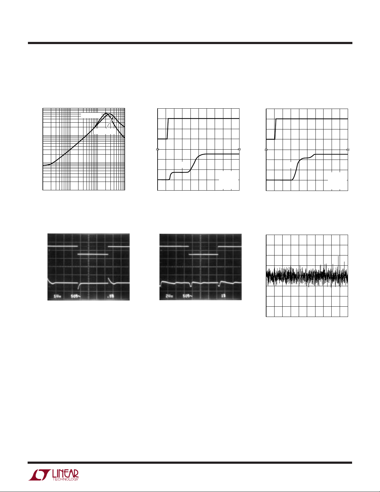
Long-Term Drift
Long-term drift cannot be extrapolated from acceler-
ated high temperature testing. This erroneous technique
gives drift numbers that are wildly optimistic. The only
way long-term drift can be determined is to measure it
over the time interval of interest. The erroneous tech-
nique uses the Arrhenius Equation to derive an acceleration factor from elevated temperature readings. The
equation is:
E
A
=
F
KT T
Ae
111
–
2
where: EA = Activation Energy (Assume 0.7)
K = Boltzmann’s Constant
T2 = Test Condition in °Kelvin
T1 = Use Condition Temperature in °Kelvin
To show how absurd this technique is, compare the
LT1461 data. Typical 1000 hour long-term drift at 30°C =
60ppm. The typical 1000 hour long-term drift at 130°C =
120ppm. From the Arrhenius Equation the acceleration
factor is:
scanned regularly and measured with an 8.5 digit DVM. As
an additional accuracy check on the DVM, a Fluke 732A
laboratory reference was also scanned. Figure 7 shows the
long-term drift measurement system. The data taken is
shown at the end of the Typical Performance Characteristics section of this data sheet. The long-term drift is the
trend line that asymptotes to a value at 2000 hours. Note
the slope in output shift between 0 hours and 1000 hours
compared to the slope between 1000 hours and 2000
hours. Long-term drift is affected by differential stresses
between the IC and the board material created during
board assembly.
PCB3
PCB2
PCB1
FLUKE
732A
LABORATORY
REFERENCE
SCANNER
8.5 DIGIT
DVM
COMPUTER
1461 F07
.
0 000086313031403
Ae
=
F
.
07
–
=
767
The erroneous projected long-term drift is:
120ppm/767 = 0.156ppm/1000 hr
For a 2.5V reference, this corresponds to a 0.39µV shift
after 1000 hours. This is pretty hard to determine (read
impossible) if the peak-to-peak output noise is larger than
this number. As a practical matter, one of the best laboratory references available is the Fluke 732A and its longterm drift is 1.5µV/mo. This performance is only available
from the best subsurface zener references utilizing specialized heater techniques.
The LT1461 long-term drift data was taken with parts that
were soldered onto PC boards similar to a “real world”
application. The boards were then placed into a constant
temperature oven with TA = 30°C, their outputs were
Figure 7. Long-Term Drift Measurement Setup
Hysteresis
The hysteresis curves found in the Typical Performance
Characteristics represent the worst-case data taken on 35
typical parts after multiple temperature cycles. As expected, the parts that are cycled over the wider –40°C to
125°C temperature range have more hysteresis than those
cycled over lower ranges. Note that the hysteresis coming
from 125°C to 25°C has an influence on the – 40°C to 25°C
hysteresis. The –40°C to 25°C hysteresis is different
depending on the part’s previous temperature. This is
because not all of the high temperature stress is relieved
during the 25°C measurement.
The typical performance hysteresis curves are for parts
mounted in a socket and represent the performance of the
12

WUUU
APPLICATIO S I FOR ATIO
LT1461
parts alone. What is more interesting are parts IR soldered
onto a PC board. If the PC board is then temperature cycled
several times from – 40°C to 85°C, the resulting hysteresis
curve is shown in Figure 8. This graph shows the influence
of the PC board stress on the reference.
When the LT1461 is soldered onto a PC board, the output
shifts due to thermal hysteresis. Figure 9 shows the effect
of soldering 40 pieces onto a PC board using standard IR
reflow techniques. The average output voltage shift is
–110ppm. Remeasurement of these parts after 12 days
shows the outputs typically shift back 45ppm toward their
initial value. This second shift is due to the relaxation of
stress incurred during soldering.
12
WORST-CASE HYSTERESIS
11
ON 35 UNITS
10
9
8
7
6
5
4
NUMBER OF UNITS
3
2
1
0
–160 –120 –80 –40
–200
HYSTERESIS (ppm)
The LT1461 is capable of dissipating high power, i.e., for
the LT1461-2.5, 17.5V • 50mA = 875mW. The SO-8
package has a thermal resistance of 190°C/W and this
dissipation causes a 166°C internal rise producing a
junction temperature of TJ = 25°C + 166°C = 191°C. What
will actually occur is the thermal shutdown will limit the
junction temperature to around 150°C. This high temperature excursion will cause the output to shift due to thermal
hysteresis. Under these conditions, a typical output shift
is –135ppm, although this number can be higher. This
high dissipation can cause the 25°C output accuracy to
exceed its specified limit. For best accuracy and preci-
sion, the LT1461 junction temperature should not exceed 125°C.
–40°C TO 25°C85°C TO 25°C
0 40 80 120 160 200
1461 F08
Figure 8. –40°C to 85°C Hysteresis of 35 Parts Soldered Onto a PC Board
12
10
8
6
4
NUMBER OF UNITS
2
0
–300
–100 0 100
–200
OUTPUT VOLTAGE SHIFT (ppm)
200 300
1461 F09
Figure 9. Typical Distribution of Output Voltage Shift After Soldering Onto PC Board
13

LT1461
WW
SI PLIFIED SCHE ATIC
100k
3SHDN
1461 SS
V
2
IN
V
6
OUT
GND
4
14

PACKAGE DESCRIPTIO
U
Dimensions in inches (millimeters) unless otherwise noted.
S8 Package
8-Lead Plastic Small Outline (Narrow 0.150)
(LTC DWG # 05-08-1610)
0.189 – 0.197*
(4.801 – 5.004)
7
8
5
6
LT1461
0.228 – 0.244
(5.791 – 6.197)
0.010 – 0.020
(0.254 – 0.508)
0.008 – 0.010
(0.203 – 0.254)
*
DIMENSION DOES NOT INCLUDE MOLD FLASH. MOLD FLASH
SHALL NOT EXCEED 0.006" (0.152mm) PER SIDE
**
DIMENSION DOES NOT INCLUDE INTERLEAD FLASH. INTERLEAD
FLASH SHALL NOT EXCEED 0.010" (0.254mm) PER SIDE
×
°
45
0.016 – 0.050
(0.406 – 1.270)
(1.346 – 1.752)
0°– 8° TYP
0.053 – 0.069
0.014 – 0.019
(0.355 – 0.483)
TYP
0.150 – 0.157**
(3.810 – 3.988)
1
3
2
4
0.004 – 0.010
(0.101 – 0.254)
0.050
(1.270)
BSC
SO8 1298
Information furnished by Linear Technology Corporation is believed to be accurate and reliable.
However, no responsibility is assumed for its use. Linear Technology Corporation makes no representation that the interconnection of its circuits as described herein will not infringe on existing patent rights.
15

LT1461
TYPICAL APPLICATIO
U
Low Power 16-Bit A/D
200µA35µA1µF
V
CC
V
REF
V
IN
= 4µV
= 6.25µV
V
CC
LTC2400
GND
= 16µV
RMS
= 24µV
RMS
RMS
F
O
SCK
SD0
CS
= 36µV
P-P
1461 TA03
P-P
P-P
SPI
INTERFACE
V
CC
LT1461-2.5
V
GND
OUT
1µF
INPUT
0.1µF
NOISE PERFORMANCE*
= 0V, V
V
IN
VIN = V
VIN = V
*FOR 24-BIT PERFORMANCE USE LT1236 REFERENCE
REF
REF
NOISE
/2, V
, V
= 1.1ppm
NOISE
NOISE
= 1.6ppm
= 2.5ppm
RMS
RMS
= 2.25µV
RMS
RELATED PARTS
PART NUMBER DESCRIPTION COMMENTS
LT1019 Precision Reference Bandgap, 0.05%, 5ppm/°C
LT1027 Precision 5V Reference Lowest TC, High Accuracy, Low Noise, Zener Based
LT1236 Precision Reference 5V and 10V Zener-Based 5ppm/°C, SO-8 Package
LTC®1798 Micropower Low Dropout Reference 0.15% Max, 6.5µA Supply Current
LT1460 Micropower Precision Series Reference Bandgap, 130µA Supply Current 10ppm/°C, Available in SOT-23
LT1634 Micropower Precision Shunt Voltage Reference Bandgap 0.05%, 10ppm/°C, 10µA Supply Current
LT1790 Precision SOT-23 Series Reference Bandgap 0.05% Max, 10ppm/°C Max
16
Linear Technology Corporation
1630 McCarthy Blvd., Milpitas, CA 95035-7417
(408) 432-1900 ● FAX: (408) 434-0507
●
www.linear-tech.com
1461f LT/LCG 0800 4K • PRINTED IN USA
LINEAR TECHNOLOGY CORPORATION 1999
 Loading...