

Linear Technology LT1308 Datasheet
Final Electrical Specifications
FEATURES
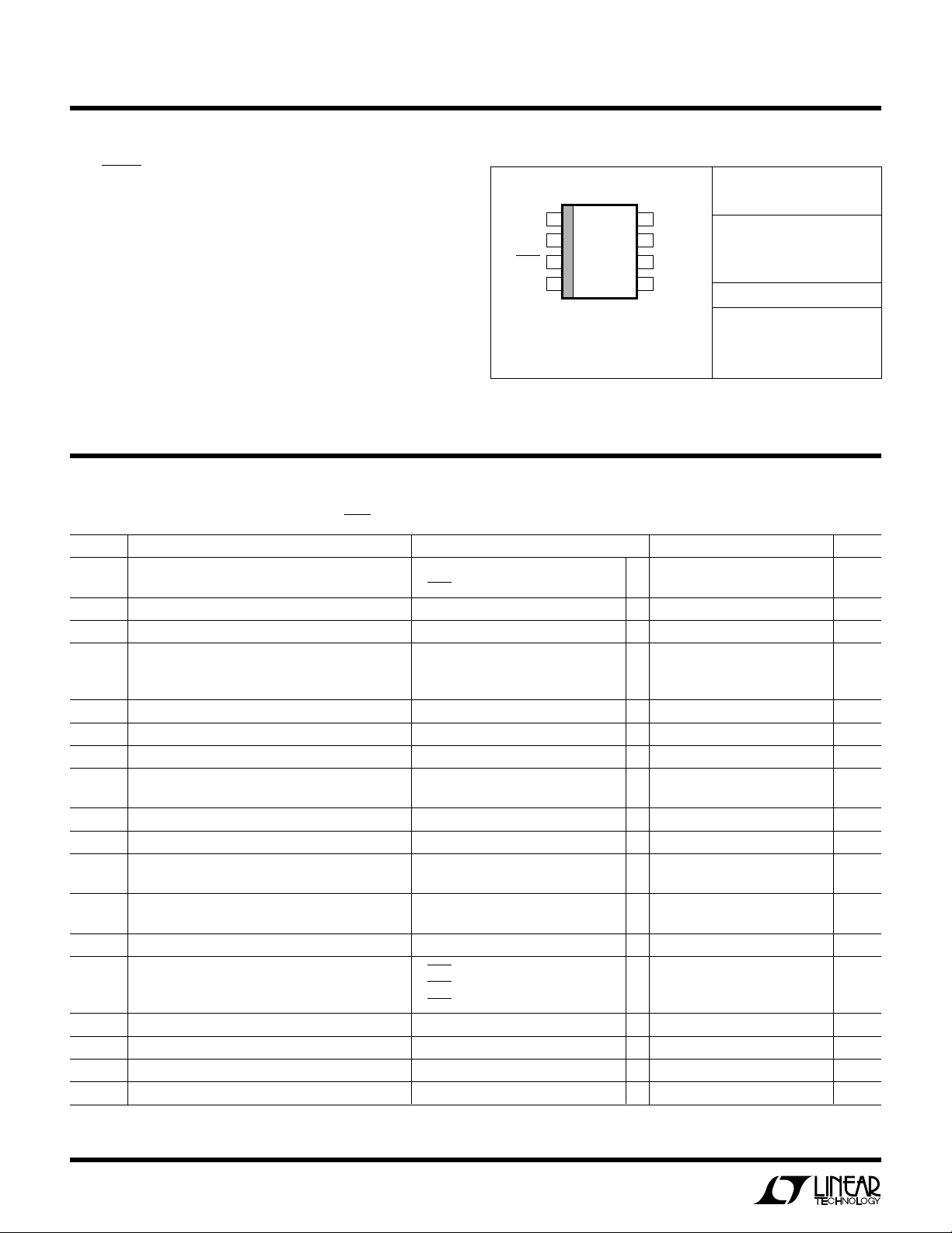
LOAD CURRENT (mA)
1
EFFICIENCY (%)
95
90
85
80
75
70
65
10 100 1000
1308 F01a
VIN = 4.2V
VIN = 3.6V
VIN = 3V
LT1308
Single Cell High Current
Micropower 600kHz
Boost DC/DC Converter
January 1998
U
DESCRIPTION
■
5V at 1A from a Single Li-Ion Cell
■
3.3V at 300mA from a Single NiCd Cell
■
Low Quiescent Current: 100µA
■
Operates with VIN as Low as 1V
■
Fixed Frequency Operation: 600kHz
■
Current Mode PWM Delivers Low Output Ripple
■
Guaranteed Start-Up into Full Load
■
Low Shutdown Current: 3µA
■
Low-Battery Comparator
■
Automatic Burst ModeTM Operation at Light Load
■
Low V
Switch: 300mV at 2A
CESAT
U
APPLICATIONS
■
GSM Terminals
■
Digital Cameras
■
Answer-Back Pagers
■
Cordless Telephones
■
DECT Phones
■
GPS Receivers
■
Battery Backup Supplies
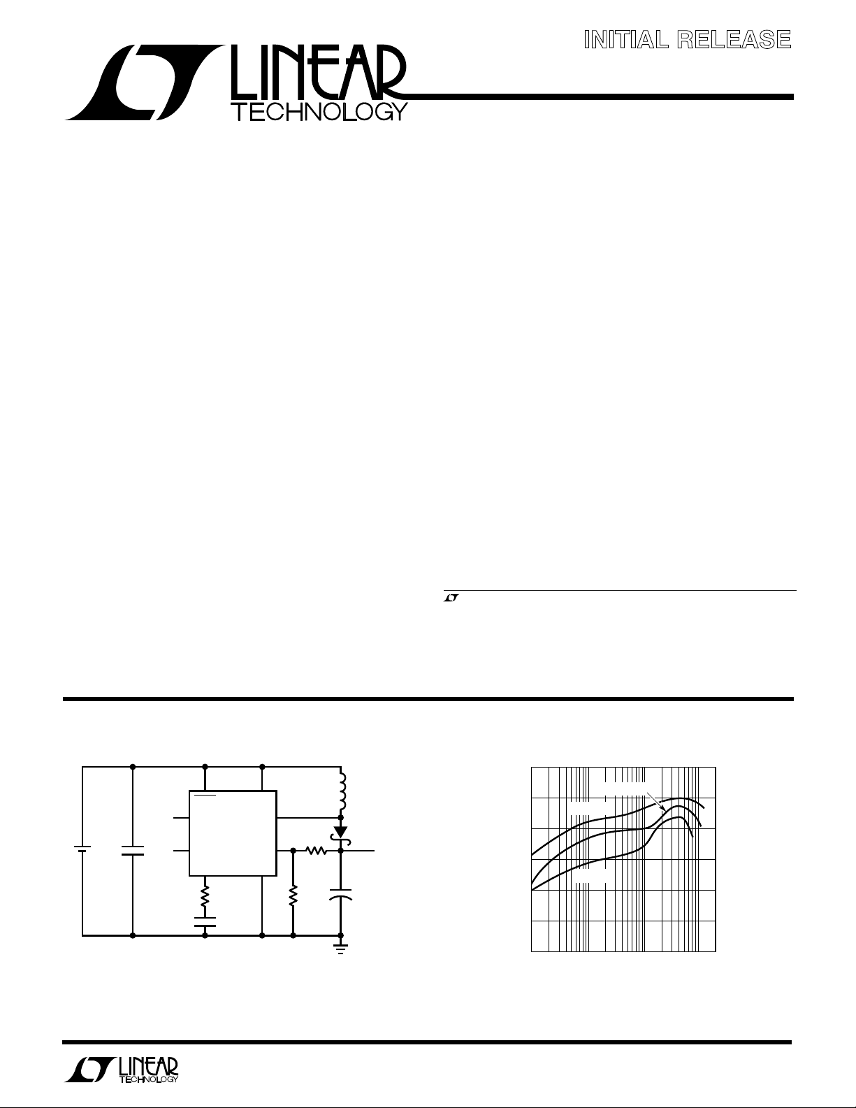
The LT®1308 is a micropower, fixed frequency boost
DC/DC converter that operates from an input voltage as
low as 1V. Capable of delivering 5V at load current of 1A
from a single Li-Ion cell, the LT1308 also features power
saving Burst Mode operation at light loads. High efficiency
is maintained over a broad 1mA to 1A load range.
The device contains a low-battery detector with a 200mV
reference and shuts down to less than 5µA quiescent
current. No-load quiescent current is 100µA and the
internal NPN power switch handles a 2A current with a
voltage drop of just 300mV.
High frequency 600kHz switching allows the use of small,
surface mount components. The LT1308’s current mode
architecture provides fast response to load and line variations. The device is available in an 8-lead SO package.
, LTC and LT are registered trademarks of Linear Technology Corporation.
Burst Mode is a trademark of Linear Technology Corporation.
TYPICAL APPLICATION
4.2V TO 3V
SHDN
LBI
Li-Ion
CELL
C1: CERAMIC
C2: AVX TPS SERIES
D1:INTERNATIONAL RECTIFIER 10BQ015
L1: COILTRONICS CTX5-1
COILCRAFT DO3316-472
Figure 1. Single Li-Ion Cell to 5V/1A DC/DC Converter
C1
10µF
LBO
U
L1
V
IN
SW
LT1308
FB
V
C
GND
R
C
47k
C
C
22nF
Information furnished by Linear Technology Corporation is believed to be accurate and reliable.
However, no responsibility is assumed for its use. Linear Technology Corporation makes no representation that the interconnection of its circuits as described herein will not infringe on existing patent rights.
301k
R2
100k
4.7µH
R1
D1
5V
1A
+
C2
100µF
1308F01
Converter Efficiency
1
LT1308
WU
NUMBER
LT1308CS8
LT1308IS8
1308
1308I
A
W
O
LUTEXI T
S
A
WUW
ARB
U
G
I
S
VIN, SHDN, LBO Voltage ......................................... 10V
SW Voltage ............................................................. 30V
FB Voltage ....................................................... VIN + 1V
VC Voltage ................................................................ 2V
LBI Voltage ............................................ 0V ≤ V
LBI
≤ 1V
Current into FB Pin .............................................. ±1mA
Junction Temperature........................................... 125°C
Operating Temperature Range
Commercial (Note 1) ......................... –20°C to 70°C
PACKAGE
TOP VIEW
V
1
C
FB
2
SHDN
3
GND
4
S8 PACKAGE
8-LEAD PLASTIC SO
T
= 125°C, θJA = 80°C/W
JMAX
/
O
RDER I FOR ATIO
ORDER PART
LBO
8
LBI
7
V
6
IN
SW
5
S8 PART MARKING
Industrial ........................................... –40°C to 85°C
Storage Temperature Range ................ – 65°C to 150°C
Consult factory for Military grade parts.
Lead Temperature (Soldering, 10 sec)................. 300°C
LECTRICAL C CHARA TERIST
E
Commercial Grade 0°C to 70°C. VIN = 1.1V, V
SYMBOL PARAMETER CONDITIONS MIN TYP MAX UNITS
I
Q
VFBFeedback Voltage ● 1.20 1.22 1.24 V
I
B
g
m
A
V
f
OSC
Quiescent Current Not Switching ● 80 160 µA
FB Pin Bias Current (Note 2) VFB = V
Reference Line Regulation 1.1V ≤ VIN ≤ 2V (25°C, 0°C) 0.6 1.1 %/V
Minimum Input Voltage 0.92 1 V
Input Voltage Range ● 16V
Error Amp Transconductance ∆I = 5µA40µmhos
Error Amp Voltage Gain 25°C, 0°C 100 V/V
Switching Frequency ● 500 600 700 kHz
Maximum Duty Cycle ● 80 88 95 %
Switch Current Limit (Note 3) DC = 40% ● 2.0 2.5 A
Switch V
CESAT
Burst Mode Operation Switch Current Limit L = 3.3µH, V
Shutdown Pin Current V
LBI Threshold Voltage ● 180 200 220 mV
LBO Output Low I
LBO Leakage Current V
LBI Input Bias Current (Note 4) V
ICS
= VIN, TA = 25°C, unless otherwise noted.
SHDN
= 0V ● 13µA
V
SHDN
REF
1.1V ≤ V
2V ≤ V
70°C 80 V/V
DC = 80% 1.6 2 A
ISW = 2A (25°C, 0°C) 300 350 mV
I
SW
SHDN
V
SHDN
V
SHDN
SINK
LBI
LBI
≤ 2V (70°C) 1.5 %/V
IN
≤ 6V ● 0.3 0.8 %/V
IN
= 2A (70°C) 330 400 mV
= 3.3V, VIN = 1.2V 200 mA
OUT
= 1.1V ● 2.5 4.0 µA
= 6V 13 26 µA
= 0V ● –1.5 –2.5 µA
= 10µA ● 0.1 0.25 V
= 250mV, V
= 150mV ● 530nA
= 5V ● 0.01 0.1 µA
LBO
● 27 80 nA
U
2
LT1308
LECTRICAL C CHARA TERIST
E
Commercial Grade 0°C to 70°C. VIN = 1.1V, V
SYMBOL PARAMETER CONDITIONS MIN TYP MAX UNITS
Low-Battery Detector Gain 1MΩ Load (25°C, 0°C) 1000 3000 V/V
Switch Leakage Current VSW = 5V ● 0.01 10 µA
Reverse Battery Current (Note 5) 750 mA
ICS
= VIN, TA = 25°C unless otherwise noted.
SHDN
1MΩ Load (70°C) 500 V/V
Commercial Grade TA = –20°C, VIN = 1.1V, V
SYMBOL PARAMETER CONDITIONS MIN TYP MAX UNITS
I
V
g
A
f
Q
FB
m
V
OSC
Quiescent Current VFB = 1.3V, Not Switching 80 160 µA
Feedback Voltage 1.195 1.22 1.245 V
Error Amp Transconductance ∆I = 5µA35µmhos
Error Amp Voltage Gain 100 V/V
Switching Frequency 500 600 750 kHz
Maximum Duty Cycle 88 %
Switch V
CESAT
Shutdown Pin Current V
LBI Threshold Voltage 180 200 220 mV
Industrial Grade –40°C to 85°C. VIN = 1.2V, V
SYMBOL PARAMETER CONDITIONS MIN TYP MAX UNITS
I
Q
VFBFeedback Voltage ● 1.195 1.22 1.245 V
I
B
g
m
A
V
f
OSC
Quiescent Current Not Switching ● 80 160 µA
FB Pin Bias Current (Note 2) VFB = V
Reference Line Regulation 1.1V ≤ VIN ≤ 2V (–40°C) 0.6 1.1 %/V
Minimum Input Voltage (–40°C) 1.2 V
Input Voltage Range ● 1.2 6 V
Error Amp Transconductance ∆I = 5µA40µmhos
Error Amp Voltage Gain –40°C 100 V/V
Switching Frequency VIN = 1.3V (–40°C) 500 600 750 kHz
Maximum Duty Cycle –40°C808895%
Switch Current Limit (Note 3) DC = 40% ● 2.0 2.5 A
Switch V
CESAT
Burst Mode Operation Switch Current Limit L = 3.3µH, V
= VIN, unless otherwise noted (Note 1).
SHDN
= 0V 1 3 µA
V
SHDN
ISW = 2A, VIN = 1.2V 300 350 mV
= V
SHDN
IN
= 0V –1.5 – 2.5 µA
V
SHDN
= VIN, TA = 25°C, unless otherwise noted.
SHDN
= 0V ● 13µA
V
SHDN
REF
1.1V ≤ V
2V ≤ V
85°C 80 V/V
V
85°C75%
DC = 80% 1.6 2 A
ISW = 2A (–40°C) 300 350 mV
I
SW
≤ 2V (85°C) 1.5 %/V
IN
≤ 6V ● 0.3 0.8 %/V
IN
= 1.3V (85°C) 500 600 750 kHz
IN
= 2A (85°C) 330 400 mV
= 3.3V 200 mA
OUT
2.5 4.0 µA
● 27 80 nA
3
 Loading...