

Linear Technology LT1305 Datasheet
LT1305
Micropower High Power
DC/DC Converter with
Low-Battery Detector
EATU
F
■
5V at 400mA from 2V Input
■
Supply Voltage As Low As 1.8V
■
120µA Quiescent Current
■
Low-Battery Detector
■
Low V
■
Uses Inexpensive Surface Mount Inductors
■
8-Lead SO Package
PPLICATI
A
■
2-Cell and 3-Cell to 5V Conversion
■
EL Panel Drivers
■
Portable Instruments
S
RE
Switch: 310mV at 2A Typ
CESAT
U
O
S
A
PPLICATITYPICAL
O
U
DUESCRIPTIO
The LT®1305 is a micropower step-up DC/DC converter
that uses Burst ModeTM operation. Similar to the LT1303,
the LT1305 features a 2A internal low-loss switch and can
deliver up to four times the output power of the LT1303.
Quiescent current is only 120µA and the Shutdown pin
further reduces current to 10µA. A low-battery detector
provides an open-collector output that goes low when the
input voltage drops below a preset level. The LT1305 is
available in an 8-pin SO, easing board space requirements.
, LTC and LT are registered trademarks of Linear Technology Corporation.
Burst Mode is a trademark of Linear Technology Corporation
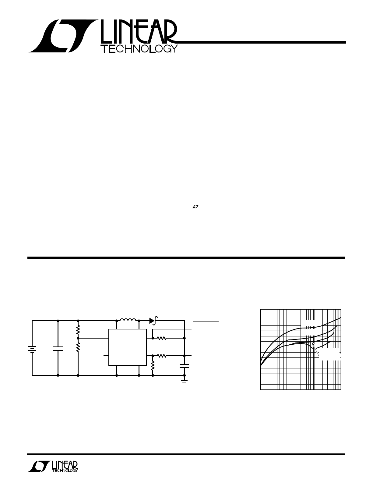
2-Cell and 3-Cell to 5V/400mA DC/DC Converter
with Low-Battery Detect
316k
1%
2 TO 3
CELLS
C1, C2: AVX TPSE227010R0100
D1: MOTOROLA MBRS130LT3
L1: COILCRAFT D03316-103
+
C1
220µF
412k
1%
SHUTDOWN
L1
10µH
V
IN
LBI
LT1305
SHDN
GND PGND
SW
LBO
Efficiency
D1
LOW BATTERY
100k
301k
100k
1%
1%
C2
220µF
FB
GOES LOW AT
= 2.2V
V
BAT
V
OUT
5V
400mA
+
LT1305 • TA03
90
80
EFFICIENCY (%)
70
60
1
VIN = 4.00V
VIN = 3.00V
= 2.00V
V
IN
VIN = 2.50V
10 100 1000
LOAD CURRENT (mA)
LT1305 • TA02
1
LT1305
WU
U
PACKAGE
/
O
RDER I FOR ATIO
W
O
A
LUTEXI T
S
VIN Voltage .............................................................. 10V
SW1 Voltage ............................................................ 25V
FB Voltage ............................................................... 10V
Shutdown Voltage ................................................... 10V
LBO Voltage............................................................. 10V
LBI Voltage .............................................................. 10V
Maximum Power Dissipation ............................. 500mW
Operating Temperature Range ..................... 0°C to 70°C
Storage Temperature Range ................. –65°C to 150°C
A
WUW
ARB
U
G
I
S
GND
LBO
SHDN
1
2
3
FB
4
T
JMAX
TOP VIEW
S8 PACKAGE
8-LEAD PLASTIC SO
= 100°C, θJA = 80°C/ W
ORDER PART
NUMBER
PGND
8
SW
7
V
6
IN
LBI
5
LT1305CS8
S8 PART MARKING
1305
Lead Temperature (Soldering, 10 sec)..................300°C
Consult factory for Industrial and Military grade parts.
LECTRICAL C CHARA TERIST
E
SYMBOL PARAMETER CONDITIONS MIN TYP MAX UNITS
I
Q
VINInput Voltage Range 1.8 1.55 V
DC Maximum Duty Cycle ● 75 86 95 %
t
ON
V
CESAT
V
SHDNH
V
SHDNL
I
SHDN
Quiescent Current V
Feedback Voltage ● 1.22 1.24 1.26 V
Comparator Hysteresis ● 6 12.5 mV
Feedback Pin Bias Current VFB = 1V ● 720 nA
Oscillator Frequency Current Limit Not Asserted 120 155 185 kHz
Oscillator TC 0.2 %/°C
Switch On Time Current Limit Not Asserted 5.6 µs
Output Line Regulation 1.8V < VIN < 6V ● 0.06 0.15 %/V
Switch Saturation Voltage ISW = 1A ● 140 280 mV
Switch Leakage Current VSW = 5V, Switch Off ● 0.1 10 µA
Peak Switch Current VIN = 2V 1.35 2 2.35 A
LBI Trip Voltage (Note 2) ● 1.21 1.24 1.27 V
LBI Input Bias Current V
LBO Output Low I
LBO Leakage Current V
Shutdown Pin High ● 1.8 V
Shutdown Pin Low 0.5 V
Shutdown Pin Bias Current V
ICS
TA = 25°C, VIN = 2.0V, unless otherwise noted.
= 0.5V, VFB = 2V ● 120 200 µA
SHDN
V
= 1.8V ● 715 µA
SHDN
● 2.0 V
● 1.20 2.50 A
VIN = 5V 1.15 2.15 A
= 1V ● 720 nA
LBI
= 100µA ● 0.11 0.4 V
LOAD
= 1.3V, V
LBI
= 5V ● 8.0 20 µA
SHDN
= 2V ● 3.0 µA
V
SHDN
= 0V ● 0.1 1 µA
V
SHDN
= 5V ● 0.1 5 µA
LBO
The ● denotes specifications which apply over the 0°C to 70°C operating
temperature range.
Note 1: Hysteresis specified is DC. Output ripple may be higher if output
capacitance is insufficient or capacitor ESR is excessive.
2
Note 2: Low-battery detector comparator is inoperative when device is in
shutdown.
W
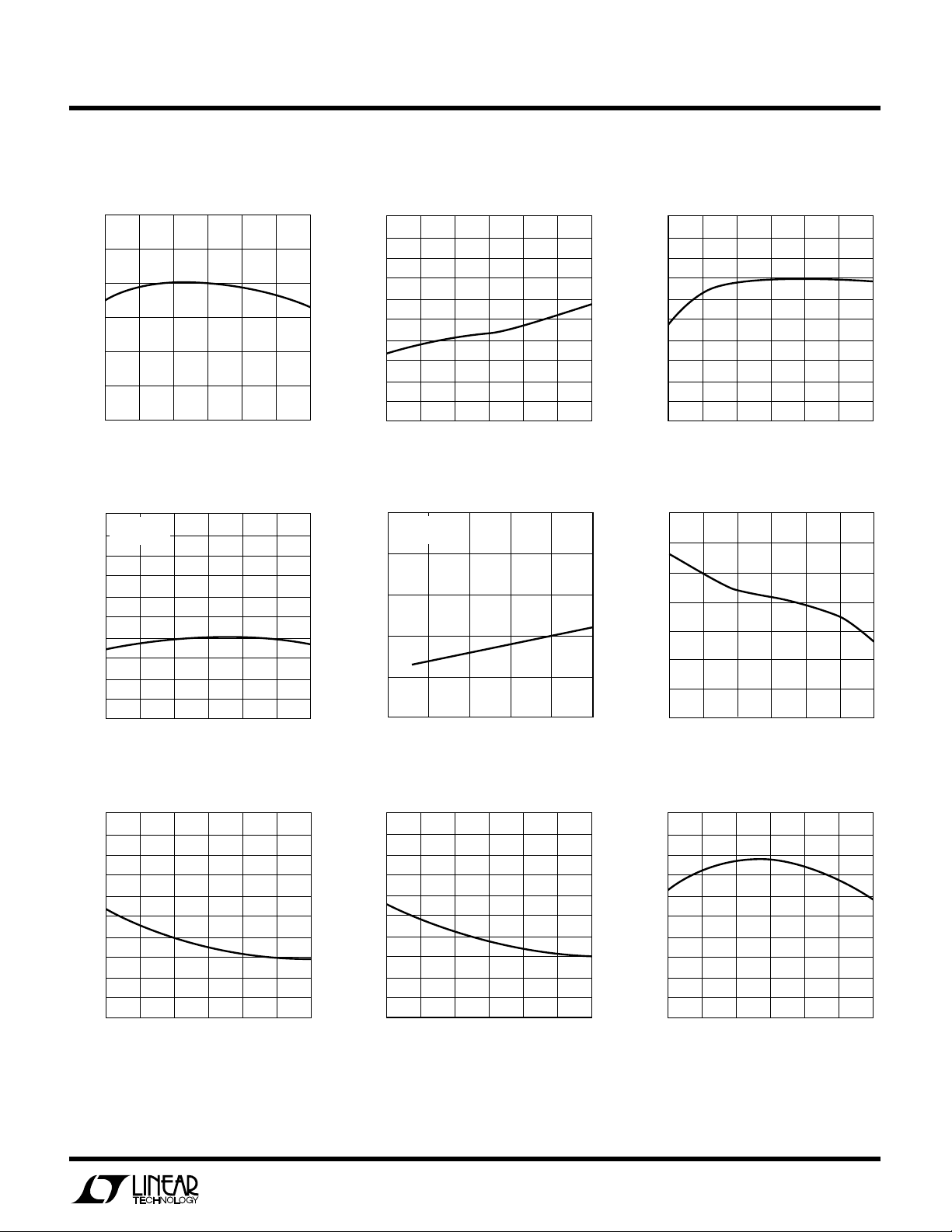
TEMPERATURE (˚C)
–50
1.8
2.0
2.2
25 75
LT1305 • G06
1.6
1.4
–25 0
50 100
1.2
1.0
PEAK SWITCH CURRENT (A)
2.4
TEMPERATURE (°C)
–50
1.200
FEEDBACK VOLTAGE (V)
1.210
1.215
1.220
1.225
1.230
1.235
–25
0
25 50
LT1305 • G09
75
1.240
1.245
1.250
1.205
100
U
TYPICAL PERFORMANCE CHARACTERISTICS
LT1305
Switch On Time
8
7
6
5
ON TIME (µs)
4
3
2
–50
–25
02550
TEMPERATURE (°C)
75 100
LT1305 • G01
Oscillator Frequency
200
190
180
170
160
150
140
FREQUENCY (kHz)
130
120
110
100
–50
–25
Quiescent Current Quiescent Current
QUIESCENT CURRENT (µA)
500
400
300
200
100
0
TA = 25°C
SWITCH OFF
0
2
200
190
180
170
160
150
140
130
QUIESCENT CURRENT (µA)
120
110
100
SWITCH OFF
V
IN
–50
= 2V
–25
TEMPERATURE (°C)
0
25 50
75
LT1305 • G04
100
25 50
0
TEMPERATURE (°C)
6
4
INPUT VOLTAGE (V)
75
LT1305 • G02
8
LT1305 • G05
100
10
Maximum Duty Cycle
100
95
90
85
80
75
70
DUTY CYCLE (%)
65
60
55
50
–50
–25
TEMPERATURE (°C)
Current Limit
0
25 50
75
LT1305 • G03
100
LBI Pin Bias Current FB Pin Bias Current
20
18
16
14
12
10
8
BIAS CURRENT (nA)
6
4
2
0
–50
–25
25 50
0
TEMPERATURE (°C)
75
LT1305 • G07
100
20
18
16
14
12
10
8
BIAS CURRENT (nA)
6
4
2
0
–50
–25
25 50
0
TEMPERATURE (°C)
75
LT1305 • G08
FB Voltage
100
3
 Loading...