

FEATURES
■
5V at 200mA from a 2V Input
■
Supply Voltage As Low As 1.8V
■
Up to 88% Efficiency
■
120µA Quiescent Current
■
Low-Battery Detector
■
Low V
■
Uses Inexpensive Surface Mount Inductors
■
8-Lead PDIP or SO Package
Switch: 170mV at 1A Typ
CESAT
U
APPLICATIONS
■
EL Panel Drivers
■
2-Cell and 3-Cell to 5V Conversion
■
Palmtop Computers
■
Portable Instruments
■
Bar-Code Scanners
■
PDAs
■
Wireless Systems
LT1303/LT1303-5
Micropower High Efficiency
DC/DC Converters with
Low-Battery Detector
Adjustable and Fixed 5V
U
DESCRIPTION
The LT®1303/LT1303-5 are micropower step-up high
efficiency DC/DC converters using Burst ModeTM operation. They are ideal for use in small, low-voltage batteryoperated systems. The LT1303-5 accepts an input voltage
between 1.8V and 5V and converts it to a regulated 5V. The
LT1303 is an adjustable version that can supply an output
voltage up to 25V. Quiescent current is only 120µA from
the battery and the shutdown pin further reduces current
to 10µA. The low-battery detector provides an open-
collector output that goes low when the input voltage
drops below a preset level. The on-chip NPN power switch
has a low 170mV saturation voltage at a switch current
of 1A. The LT1303/LT1303-5 are available in 8-lead PDIP
or SO packages, easing board space requirements.
For higher output current, please see the LT1305 or
LT1302.
, LTC and LT are registered trademarks of Linear Technology Corporation.
Burst Mode is a trademark of Linear Technology Corporation.
U
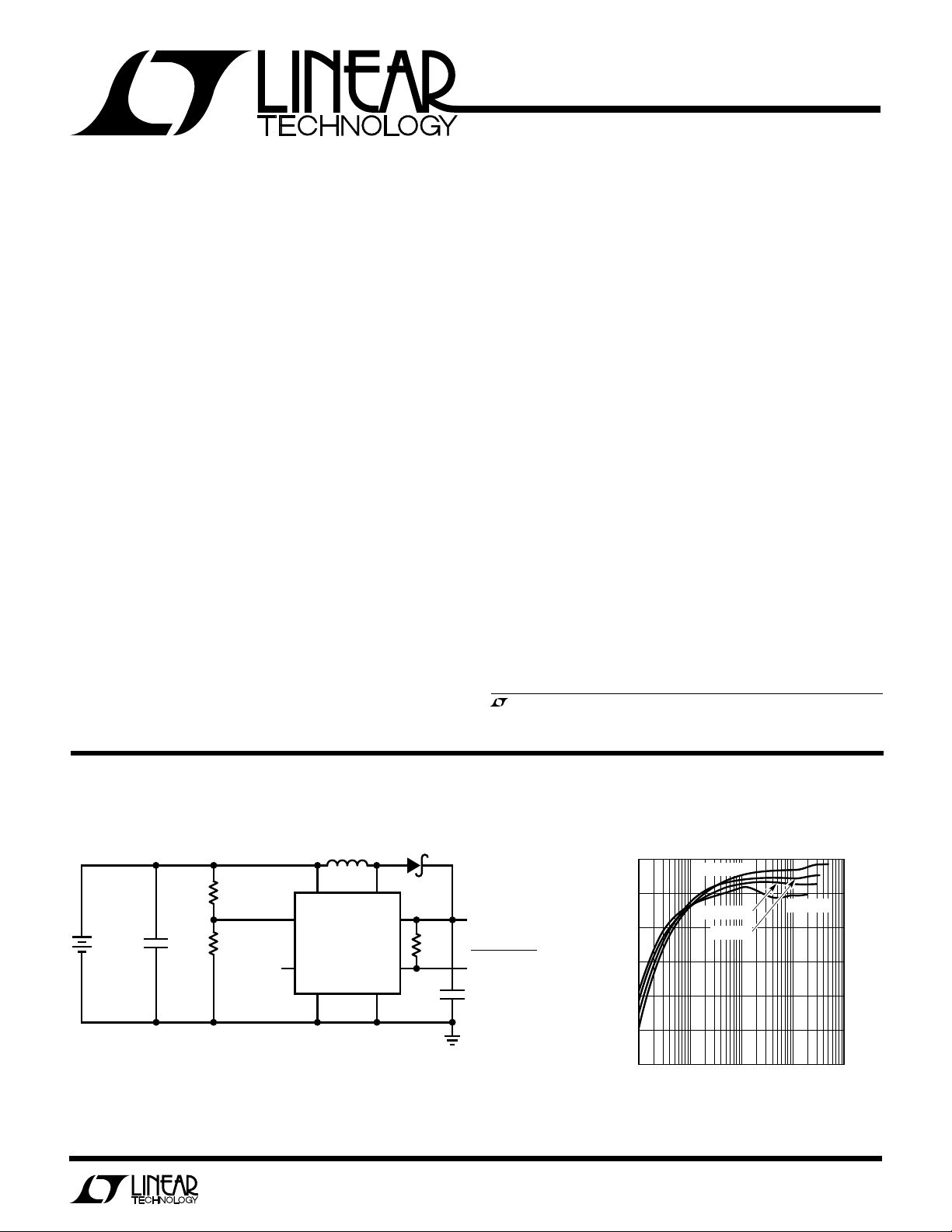
TYPICAL APPLICATION
L1
22µH
316k
+
2 CELLS
L1 = SUMDIA CD54-220
100µF
1%
412k
1%
SHUTDOWN
V
IN
LT1303-5
GND PGND
Figure 1. 2-Cell to 5V DC/DC Converter with Low-Battery Detect
1N5817
SW
SENSELBI
LBOSHDN
100µF
100k
+
, 5V
V
OUT
200mA
LOW BATTERY
GOES LOW AT
= 2.2V
V
BAT
LT1303 TA02
90
80
70
60
EFFICIENCY (%)
50
40
30
0.1
5V Output Efficiency
VIN = 4V
VIN = 2.5V
VIN = 3V
1 10010 1000
LOAD CURRENT (mA)
VIN = 2V
LT1303 TA01
1
LT1303/LT1303-5
WW
W
ABSOLUTE MAXIMUM RATINGS
V
Voltage .............................................................. 10V
IN
SW1 Voltage ............................................................ 25V
Sense Voltage (LT1303-5) ....................................... 20V
FB Voltage (LT1303)................................................ 10V
Shutdown Voltage ................................................... 10V
LBO Voltage............................................................. 10V
LBI Voltage .............................................................. 10V
Maximum Power Dissipation ............................. 500mW
Operating Temperature Range ..................... 0°C to 70°C
Storage Temperature Range ................. –65°C to 150°C
Lead Temperature (Soldering, 10 sec)..................300°C
LECTRICAL C CHARA TERIST
E
SYMBOL PARAMETER CONDITIONS MIN TYP MAX UNITS
I
Q
VINInput Voltage Range 1.8 1.55 V
DC Maximum Duty Cycle ● 75 86 95 %
t
ON
V
CESAT
V
SHDNH
V
SHDNL
I
SHDN
The
temperature range.
Quiescent Current V
Feedback Voltage LT1303 ● 1.22 1.24 1.26 V
Output Sense Voltage LT1303-5 ● 4.8 5.0 5.2 V
Comparator Hysteresis LT1303 (Note 1) ● 6 12.5 mV
Output Hysteresis LT1303-5 (Note 1) ● 22 50 mV
Feedback Pin Bias Current LT1303, VFB = 1V ● 720 nA
Oscillator Frequency Current Limit Not Asserted 120 155 185 kHz
Oscillator TC 0.2 %/°C
Switch On Time Current Limit Not Asserted 5.6 µs
Output Line Regulation 1.8V < VIN < 6V ● 0.06 0.15 %/V
Switch Saturation Voltage ISW = 700mA ● 130 200 mV
Switch Leakage Current VSW = 5V, Switch Off ● 0.1 10 µA
Peak Switch Current VIN = 2V ● 0.75 1.0 1.25 A
LBI Trip Voltage ● 1.21 1.24 1.27 V
LBI Input Bias Current V
LBO Output Low I
LBO Leakage Current V
Shutdown Pin High ● 1.8 V
Shutdown Pin Low 0.5 V
Shutdown Pin Bias Current V
● denotes specifications which apply over the 0°C to 70°C operating
SHDN
V
SHDN
VIN = 5V 0.65 0.9 1.15 A
LBI
LOAD
LBI
SHDN
V
SHDN
V
SHDN
U
U
W
PACKAGE/ORDER INFORMATION
TOP VIEW
GND
1
LBO
2
SHDN
3
FB (SENSE)*
Consult factory for Industrial and Military grade parts.
ICS
TA = 25°C, VIN = 2.0V, unless otherwise noted.
= 0.5V, V
= 1.8V ● 715 µA
= 1V ● 720 nA
= 100µA ● 0.11 0.4 V
= 1.3V, V
= 5V ● 8.0 20 µA
= 2V ● 3.0 µA
= 0V ● 0.1 1 µA
= 5V, V
SEL
= 5V ● 0.1 5 µA
LBO
= 5.5V ● 120 200 µA
SENSE
Note 1: Hysteresis specified is DC. Output ripple may be higher if output
capacitance is insufficient or capacitor ESR is excessive.
4
N8 PACKAGE
8-LEAD PDIP
S8 PACKAGE
8-LEAD PLASTIC SO
*FIXED VERSION
= 100°C, θJA = 130°C/W (N8)
T
JMAX
= 100°C, θJA = 150°C/W (S8)
T
JMAX
PGND
8
SW
7
V
6
IN
LBI
5
● 2.0 V
ORDER PART
NUMBER
LT1303CN8
LT1303CS8
LT1303CN8-5
LT1303CS8-5
S8 PART MARKING
1303
13035
U
2
W
TEMPERATURE (˚C)
–50
700
800
900
25 75
LT1303 GO3
600
500
–25 0
50 100
400
300
RESISTANCE (kΩ)
1000
TEMPERATURE (°C)
–50
1.200
LBI VOLTAGE (V)
1.210
1.215
1.220
1.225
1.230
1.235
–25
0
25 50
LT1303 G06
75
1.240
1.245
1.250
1.205
100
TEMPERATURE (°C)
–50 –25 25 75
0.60
SWITCH CURRENT (A)
0.70
0.90
1.00
1.10
50
1.50
LT1303 G09
0.80
0 100
1.20
1.30
1.40
VIN = 2V
U
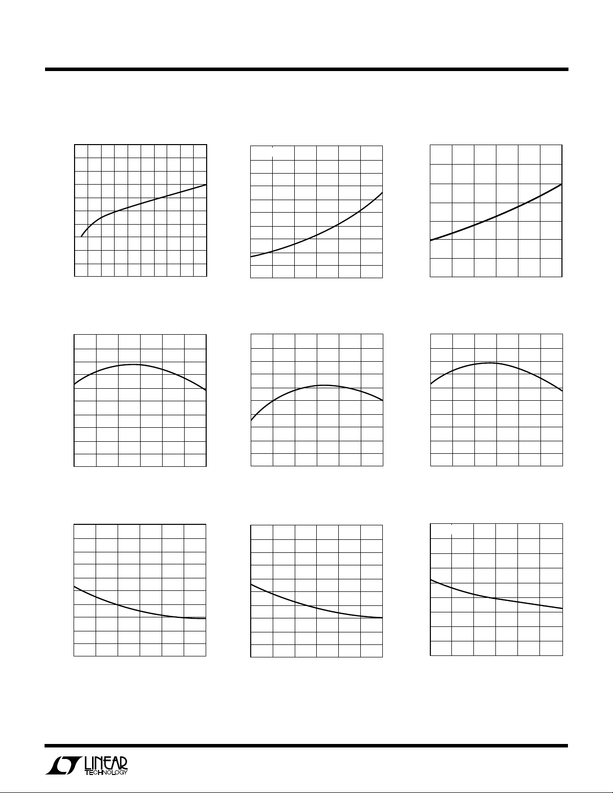
TYPICAL PERFORMANCE CHARACTERISTICS
LT1303/LT1303-5
V
vs Switch Current
CESAT
250
225
200
175
150
(mV)
125
CESAT
100
V
75
50
25
0
0.21.0 0.3 0.5 0.7 0.9
0.1
SWITCH CURRENT (A)
LT1303 FB Voltage
1.250
1.245
1.240
1.235
1.230
1.225
1.220
1.215
FEEDBACK VOLTAGE (V)
1.210
1.205
1.200
–50
–25
TEMPERATURE (°C)
0
0.4
0.6
25 50
0.8
LT1303 G01
75
LT1330 G04
1.0
100
V
vs Temperature
CESAT
200
ISW = 700mA
190
180
170
160
(mV)
150
CESAT
140
V
130
120
110
100
–50
–25
5.10
5.08
5.06
5.04
5.02
5.00
4.98
SENSE VOLTAGE (V)
4.96
4.94
4.92
4.90
–50
–25
25 50
0
TEMPERATURE (°C)
25 50
0
TEMPERATURE (°C)
75
LT1303 G02
75
LT1303 G05
LT1303-5 Sense Pin Resistance
to Ground
100
Low Battery Detect Trip PointLT1303-5 Sense Voltage
100
LBI Pin Bias Current
20
18
16
14
12
10
8
BIAS CURRENT (nA)
6
4
2
0
–50
–25
25 50
0
TEMPERATURE (°C)
75
LT1303 G07
100
FB Pin Bias Current
20
18
16
14
12
10
8
BIAS CURRENT (nA)
6
4
2
0
–50
–25
25 50
0
TEMPERATURE (°C)
75
LT1303 G08
100
Switch Current Limit
3
LT1303/LT1303-5
W
U
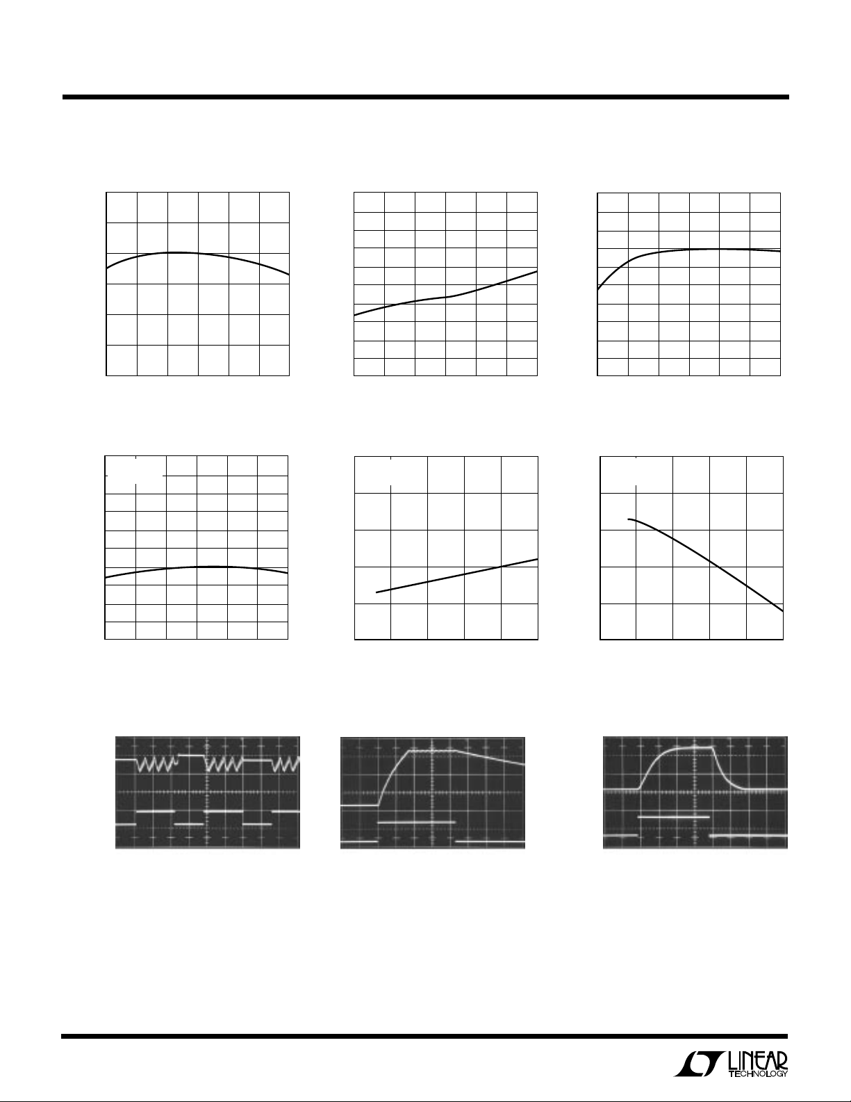
TYPICAL PERFORMANCE CHARACTERISTICS
Switch On-Time Maximum Duty Cycle
8
7
6
5
ON-TIME (µs)
4
3
2
–50
02550
–25
TEMPERATURE (°C)
75 100
LT1303 G10
Oscillator Frequency
200
190
180
170
160
150
140
FREQUENCY (kHz)
130
120
110
100
–50
–25
TEMPERATURE (°C)
0
25 50
75
LT1303 G11
100
100
95
90
85
80
75
70
DUTY CYCLE (%)
65
60
55
50
–50
–25
TEMPERATURE (°C)
Quiescent Current Quiescent Current Switch Current Limit
200
190
180
170
160
150
140
130
QUIESCENT CURRENT (µA)
120
110
100
SWITCH OFF
V
IN
–50
= 2V
–25
TEMPERATURE (°C)
0
25 50
75
LT1303 G13
100
QUIESCENT CURRENT (µA)
500
400
300
200
100
0
TA = 25°C
SWITCH OFF
0
2
4
INPUT VOLTAGE (V)
6
8
10
LT1303 G14
1200
L = 33µH
= 3V
V
L
1100
1000
900
SWITCH CURRENT (mA)
800
700
2
0
INPUT VOLTAGE (V)
0
25 50
4
100
75
LT1303 G12
6
8
10
LT1303 G15
V
OUT
100mV/DIV
AC COUPLED
200mA
I
LOAD
0mA
4
Transient Response
Figure 1 Circuit
VIN = 2V
V
= 5V
OUT
200µs/DIV
LT1303 G16
Shutdown Pin Response
5V
V
OUT
1V/DIV
V
SHDN
5V/DIV
R
= 100Ω
LOAD
V
= 2V
IN
V
= 5V
OUT
= 100µF
C
OUT
500µs/DIV
LT1303 G17
Low Battery Detector Transient
Response
V
LBO
2V/DIV
+10mV
V
TRIP
V
LBI
V
–10mV
TRIP
R
PULL-UP
= 47k
5µs/DIV
LT1303 G18

UUU
PIN FUNCTIONS
LT1303/LT1303-5
GND (Pin 1): Signal Ground. Tie to PGND under the
package.
LBO (Pin 2): Open-Collector Output of Low-Battery Comparator. Can sink 100µA. Disabled when device is in
shutdown.
SHDN (Pin 3): Shutdown. Pull high to shut down the
device. Ground for normal operation.
FB/Sense (Pin 4):
On 1303 (adjustable) this pin connects
to the main comparator C1 input. On LT1303-5 this pin
connects to the resistor string that sets output voltage
at 5V.
W
BLOCK
IDAGRA
V
IN
S
V
C1 C2
IN
6 7
LBI (Pin 5): Low-Battery Comparator Input. When voltage
on this pin below 1.24V, LBO is low.
VIN (Pin 6): Supply Pin. Must be bypassed with a large
value electrolytic to ground. Keep bypass within 0.2" of the
device.
SW (Pin 7): Switch Pin. Connect inductor and diode here.
Keep layout short and direct to minimize radio frequency
interference.
PGND (Pin 8): Power ground. Tie to signal ground (pin1)
under the package. Bypass capacitor from VIN should be
tied directly to PGND within 0.2" of the device.
SW
D1
++
L1
CURRENT
COMPARATOR
R1
FB
4
R2
REFERENCE
1.24V
HYSTERETIC
COMPARATOR
–
C1
+
OFF
OSCILLATOR
A3
DRIVER
18mV
+
C2
–
R1
3Ω
Q2
1×
Q1
160×
–
C3
+
LBOLBIGND
1
25
SHUTDOWN
3
PGND
8
LT1303 BD01
Figure 2. LT1303 Block Digram
5

LT1303/LT1303-5
BLOCK
IDAGRA
W
S
U
OPERATION
FB SW
4
R1
474k
R2
156k
V
IN
6 7
18mV
+
C2
–
HYSTERETIC
COMPARATOR
CURRENT
COMPARATOR
OFF
–
A3
DRIVER
REFERENCE
1.24V
C1
OSCILLATOR
+
R1
3Ω
Q2
1×
–
C3
+
LBOLBIGND
1
25
SHUTDOWN
3
Figure 3. LT1303-5 Block Diagram
Q1
160×
8
PGND
LT1303 BD02
Operation of the LT1303 is best understood by referring to
the Block Diagram in Figure 2. When C1’s negative input,
related to the output voltage by the appropriate resistordivider ratio, is higher than the 1.24V reference voltage,
C1’s output is low. C2, A3 and the oscillator are turned off,
drawing no current. Only the reference and C1 consume
current, typically 140µA. When C1’s negative input drops
below 1.24V and overcomes C1’s 6mV hysteresis, C1’s
output goes high, enabling the oscillator, current comparator C2 and driver A3. Quiescent current increases to 2mA
as the device goes into active switching mode. Q1 then
turns on in controlled saturation for nominally 6µ s or until
current comparator C2 trips, whichever comes first. The
switch then turns off for approximately 1.5µ s, then turns on
again. The LT1303’s switching causes current to alternately build up in L1 and dump into output capacitor C4 via
D1, increasing the output voltage. When the output is high
enough to cause C1’s output to go high, switching action
ceases. Capacitor C4 is left to supply current to the load
until V
decreases enough to force C1’s output high, and
OUT
the entire cycle repeats. Figure 4 details relevant waveforms. C1’s cycling causes low-to-mid-frequency ripple
voltage on the output. Ripple can be reduced by making the
output capacitor large. The 100µ F unit specified results in
ripple of 50mV to 100mV on the 5V output. A 220µF
capacitor will decrease ripple by approximately 50%.
V
OUT
100mV/DIV
AC COUPLED
V
SW
5V/DIV
I
L
1A/DIV
20µs/DIV
LT1303 F04
Figure 4. Burst Mode Operation in Action
If switch current reaches 1A, causing C2 to trip, switch ontime is reduced and off-time increases slightly. This allows
continuous operation during bursts. C2 monitors the
voltage across 3Ω resistor R1 which is directly related to
the switch current. Q2’s collector current is set by the
emitter-area ratio to 0.6% of Q1’s collector current. When
R1’s voltage drop exceeds 18mV, corresponding to 1A
switch current, C2’s output goes high, truncating the ontime portion of the oscillator cycle and increasing off-time
6

U
OPERATION
LT1303/LT1303-5
to about 2µs. Response time of C2, which determines
minimum on-time, is approximately 300ns.
Low Battery Detector
The low battery detector is enabled when SHDN is low and
disabled when SHDN is high. The comparator has no
V
BAT
R1
1.24V
LT1303
–
+
R2
49.9k
1%
R1 = (V
HYSTERESIS ≈ 30mV
–1.24V) (43.5k)
TRIP
2M
R3
Figure 5. R3 Adds Hysteresis to Low-Battery Detector
U
WUU
5V
LT1303 F05
R4
47k
APPLICATIONS INFORMATION
hysteresis built in, but hysteresis can be added by
connecting a high-value resistor from LBI to LBO as
shown in Figure 5. The internal reference can be accessed
via the comparator as shown in Figure 6.
V
IN
100k
2N3906
V
REF
OUTPUT
= 1.24V 1 +
V
REF
VIN ≥ V
REF
R1 + R2 ≈ 33k
R2
+
2.2µF
R2
()
R1
+ 200mV
Figure 6. Accessing Internal Reference
V
IN
LBO
LT1303
LBI
GND
R1
LT1303 F06
Inductor Section
Inductors suitable for use with the LT1303 usually fall in
the 5µH to 50µH range. The inductor must: (1) handle
current of 1.25A without saturating, (2) have enough
inductance to provide a di/dt lower than 400mA/µs, and
(3) have low enough DC resistance to avoid excessive
heating or efficiency losses. Higher value inductors will
deliver more power but tend to be physically larger. Most
ferrite core drum or rod inductors such as those specified
in Table 1 are suitable for use. It is acceptable to bias openflux inductors (e.g. Sumida CD54) into saturation by 10 to
20% without adverse effects.
Table 1. Recommended Inductors
PHONE
VENDOR SERIES APPROPRIATE VALUES NUMBERS
Coilcraft D03316 10µH to 47µH (708) 639-6400
D01608 10µH
Coiltronics OCTAPAK (407) 241-7876
CTX20-1 20µH
CTX20-2 20µH
CTX33-4 33µH
Sumida CD54 10µH to 33µH (708) 956-0666
Gowanda GA10 10µH to 33µH (716) 532-2234
Figure 7 shows inductor current of a suitable inductor,
di/dt is controlled at all times. The rapid rise in current
shown in Figure 8 results from this inductor saturating at
approximately 1A. Saturation occurs when the inductor
cannot hold any more magnetic energy in the core. Current
then increases rapidly, limited only by the resistance of the
winding. Figure 9’s inductor has high DC resistance which
results in the exponential time constant shape of the
inductor current.
I
L
500mA/DIV
5µs/DIV
Figure 7. Properly Chosen Inductor Does Not Saturate
LT1303 F07
7

LT1303/LT1303-5
U
WUU
APPLICATIONS INFORMATION
LT1303 F08
Figure 8. This Inductor Saturates at IL≈1A. A Poor Choice
LT1303 F09
Figure 9. Slight Exponential Shape to Inductor Current
Waveform Indicates Excessive DC Resistance
Capacitor Selection
Input and output capacitors should have low ESR for best
efficiency. Recommended capacitors include AVX TPS
series, Sprague 595D series, and Sanyo OS-CON. The
output capacitor’s ESR determines the high frequency
ripple amplitude. A 100µF capacitor is the minimum rec-
ommended for a 5V output. Higher output voltages can use
lower capacitance values. For example, a 12V output can
use a 33µF or 47µF capacitor. The V
pin of the LT1303
IN
should be decoupled with a 47µ F or 100µ F capacitor at the
pin. When driving a transformer, an additional decoupling
network of 10Ω and 0.1µF ceramic is recommended as
shown in Figure 10.
V
IN
10Ω
+
47µF
0.1µF
CERAMIC
V
IN
LT1303
SW
• • •
Diode Selection
The LT1303’s high switching speed demands a high speed
rectifier. Schottky diodes are preferred for their low forward drop and fast recovery. Suitable choices include the
1N5817, MBRS120LT3, and MBR0520LT1. Do not use
signal diodes such as 1N4148. They cannot carry 1A
current. Also avoid “general-purpose” diodes such as
1N4001. These are far too slow and are unsuitable for any
switching regulator application. For high temperature
applications a silicon diode such as the MUR105 will have
less leakage.
GND PGND
LT1303 F10
Figure 10. 10Ω-1µF Network to LT1303 VIN Pin Provides
Additional Decoupling. Recommended When Driving
Transformers.
Table 2. Recommended Capacitors
PHONE
VENDOR SERIES TYPE NUMBERS
AVX TPS Surface Mount (803) 448-9411
Sanyo OS-CON Through-Hole (619) 661-6835
Panasonic HFQ Through-Hole (201) 348-5200
Sprague 595D Surface Mount (603) 224-1961
8

U
TYPICAL APPLICATIONS
LT1303/LT1303-5
Setting Output Voltage on LT1303
INPUT
1.8V TO 4.5V
V
OUTPUT
REF
1.24V
V
IN
+
100µF
V
= 1.24V 1 +
OUT
L1
V
IN
R2
()
R1
SW
LT1303
PGNDGND
1N5817
FB
5V Step-Up Converter with Reference Output
22µH*
2N3906
+
2.2µF
33k
100k
V
IN
100µF
LBO
LT1303-5
GND PGND
+
R2
R1
SW
SENSE
SHDNLBI
V
+
100µF
1303 TA03
1N5817
OUT
OUTPUT
5V
+
100µF
* SUMIDA CD54-220MC
1303 TA04
9

LT1303/LT1303-5
U
TYPICAL APPLICATIONS
4-, 5-Cell to 5V Converter with Output Disconnect
510Ω
SW
SENSE
SHDN
MBRS130T3
SHUTDOWN
+
ZTX788B
33µF
V
OUT
5V
100mA
+
220µF**
LT1303TA05
V
2V TO 8V
IN
+
33µF
SUMIDA CD54-100MC
*
AVX TPS 220µF/10V
**
10µH*
V
IN
LT1303-5
GND PGND
3-Cell to 3.3V Boost/Linear Converter with Output Disconnect
10
VIN
2V TO 6V
SHUTDOWN
+
SUMIDA CD54-100MC
*
AVX TPS 330µF/6.3V
**
†
1% METAL FILM
33µF
10µH*
V
IN
SHDN
LT1303
LBI
GND PGND
MBRS130T3
SW
LB0
FB
1.96k
121k
100k
†
Si9433
100Ω
+
33µF
†
200k
†
V
3.3V/200mA
OUT
+
330µF**
× 2
LT1303 TA07

U
TYPICAL APPLICATIONS
V
IN
1.5V TO 8V
+
47µF
0.1µF
CERAMIC
SHUTDOWN
10Ω
V
IN
LT1303
SHDN
GND PGND
EL Panel Driver
T1**
MUR160
6
•
10
1N5818
3.3M
3.3M
FB
51k
†
R1
25k
4,5
1,2
1:15
•
SW
3.3M
1N4148
10k
LT1303/LT1303-5
C1*
50pF
4.7µF
160V
+
1k
1/2W
MPSA42
EL PANEL
100Hz TO 1000Hz
SQUARE WAVE
DRIVE
*
ADD C1 FOR OPEN-PANEL PROTECTION
**
DALE LPE5047-A132 1:15 TURNS RATIO (605) 666-9301
†
R1 ADJUSTS V
OUT
83V
RMS
TO 115V
RMS
LT1303 TA06
Information furnished by Linear Technology Corporation is believed to be accurate and reliable.
However, no responsibility is assumed for its use. Linear Technology Corporation makes no representation that the interconnection of circuits as described herein will not infringe on existing patent rights.
11

LT1303/LT1303-5
PACKAGE DESCRIPTION
0.300 – 0.325
(7.620 – 8.255)
U
Dimensions in inches (millimeters) unless otherwise noted.
N8 Package
8-Lead Plastic DIP
0.045 – 0.065
(1.143 – 1.651)
0.130 ± 0.005
(3.302 ± 0.127)
0.400*
(10.160)
MAX
876
5
0.065
(1.651)
0.009 – 0.015
(0.229 – 0.381)
+0.025
0.325
–0.015
+0.635
8.255
()
–0.381
*THESE DIMENSIONS DO NOT INCLUDE MOLD FLASH OR PROTRUSIONS.
MOLD FLASH OR PROTRUSIONS SHALL NOT EXCEED 0.010 INCH (0.254mm)
0.010 – 0.020
(0.254 – 0.508)
0.008 – 0.010
(0.203 – 0.254)
*
DIMENSION DOES NOT INCLUDE MOLD FLASH. MOLD FLASH
SHALL NOT EXCEED 0.006" (0.152mm) PER SIDE
**
DIMENSION DOES NOT INCLUDE INTERLEAD FLASH. INTERLEAD
FLASH SHALL NOT EXCEED 0.010" (0.254mm) PER SIDE
× 45°
0.016 – 0.050
0.406 – 1.270
TYP
0.005
(0.127)
MIN
0.100 ± 0.010
(2.540 ± 0.254)
0.053 – 0.069
(1.346 – 1.752)
0°– 8° TYP
0.014 – 0.019
(0.355 – 0.483)
0.125
(3.175)
MIN
0.018 ± 0.003
(0.457 ± 0.076)
S8 Package
8-Lead Plastic SOIC
0.004 – 0.010
(0.101 – 0.254)
0.050
(1.270)
BSC
0.015
(0.380)
MIN
0.228 – 0.244
(5.791 – 6.197)
0.255 ± 0.015*
(6.477 ± 0.381)
8
1
12
0.189 – 0.197*
(4.801 – 5.004)
7
6
3
2
4
3
N8 0695
5
0.150 – 0.157**
(3.810 – 3.988)
4
SO8 0695
RELATED PARTS
PART NUMBER DESCRIPTION COMMENTS
LT1129 Micropower Low Dropout Regulator 700mA Output Current in SO-8 Package
LT1182/83/84 LCD and CCFL Backlight Controller High Efficiency and Excellent Backlight Control Range
LT1301 5V to 12V/200mA Step-Up DC/DC Converter 120µA Quiescent Current
LT1302 2-Cell to 5V/600mA Step-Up DC/DC Converter 200µA Quiescent Current
LT1305 Micropower 2A Switch DC/DC Converter with Low-Battery Detect 2V to 5V at 400mA
LT1372 500kHz Step-Up PWM, 1.5A Switch Low Noise, Fixed Frequency Operation
LTC®1472 PCMCIA Host Switch with Protection Includes Current Limit and Thermal Shutdown
LT/GP 0195 10K • PRINTED IN USA
LINEAR TECHNOLOGY CORPORATION 1995
12
Linear Technology Corporation
1630 McCarthy Blvd., Milpitas, CA 95035-7487
(408) 432-1900
●
FAX
: (408) 434-0507
●
TELEX
: 499-3977
 Loading...