


Applications of the LT1300 and LT1301
Micropower DC/DC Converters
Dale Eagar and Steve Pietkiewicz
INTRODUCTION
Application Note 59
January 1994
The design of battery-powered equipment can often be
quite challenging. Since few ICs can operate directly from
the end-of-life voltage from a 2-cell battery (about 1.8V),
most systems require a DC/DC converter. The system
designer often has a limited area in which to place the DC/
DC converter; associated inductors and capacitors must be
small. Surface mount components are a must and heat
sinks are out of the question! The LT1300 and LT1301
micropower DC/DC converter ICs provide new possibilities
for more efficient, compact and cost effective designs.
When designing equipment for battery-powered
operation, a number of important design constraints
should be considered. Some of these are detailed in the
check list given here:
• Design for high efficiency. A high efficiency converter
increases battery life, eliminates most heat sinks, reduces
weight and decreases PC board area. The designer
should strive for high efficiency at:
– Full Load
– Light Load
• Plan to utilize all the capacity of the battery. Can the
circuit run down to the “dead cell” voltage? Is there a
micropower shutdown mode?
• Can the DC/DC converter circuitry provide high output
power for short time intervals? Often this is a requirement
on battery-powered equipment.
• Cost. Is the complete circuit cost competitive?
• Does the design meet packaging constraints?
– Height
– PC Board Area
– Weight
The LT1300 family of DC/DC converters allows a maximum
of flexibility in the design of circuits which provide
solutions for battery-operated and other equipment
needing high efficiency, space efficient, micropower
power solutions.
INDEX TO LT1300 CIRCUITS
Figure Description Page
1 LT1300/LT1301 Block Diagram ................................................................................................................ 2
2 2-Cell to 5V DC/DC Converter Delivers >200mA with a 2V Input .............................................................. 3
8 Lower Power Applications Can Use Smaller Components. L1 is Tallest Component at 3.1mm ................ 5
11 4-Cell to 3.3V or 5V Converter Output Goes to Zero When in Shutdown .................................................. 6
13 LT1301 Delivers 12V From 3.3V or 5V Input ............................................................................................ 7
15 Flame Detector.......................................................................................................................................... 8
16, 17 Voltage Buffer ....................................................................................................................................... 8, 9
18 CCFL Driver............................................................................................................................................. 10
19 Electronic Light Stick .............................................................................................................................. 11
20 Backlight LED Driver ............................................................................................................................... 11
21 Efficiency of LED Driver .......................................................................................................................... 12
AN59-1
Application Note 59
NEW LT1300 AND LT1301 MICROPOWER
DC/DC CONVERTERS
by Steve Pietkiewicz
Introduction
The new LT1300 and LT1301 micropower DC/DC converters provide improvements in both electrical and physical
efficiency, two key areas of battery-based power supply
design. Housed in 8-lead DIP or SOIC packages, the
devices feature a 1A on-chip switch with a V
CESAT
of just
170mV. The internal oscillator frequency is set at 155kHz,
allowing the use of tiny, 5mm diameter surface mount
inductors along with standard D-case size tantalum capacitors. A complete 2-cell to 12V, 5V, or 3.3V converter
can fit in less than 0.4 square inches of PC board area.
The devices use Burst ModeTM operation to maintain high
efficiency across the full load range. The fully operating
quiescent current is only 120µ A. It can be further reduced
to 10µA by taking the SHUTDOWN pin high, which also
disables the device. The output voltage of the LT1300 can
be set at either 5V or 3.3V via the logic-controlled SELECT
pin, and the LT1301 output can be set at either 5V or 12V
using the same pin. The I
pin allows the reduction of
LIM
peak switch current and allows the use of even smaller
components. The switch current is nominally set at 1A and
can be reduced via the I
pin to approximately 400mA,
LIM
further improving efficiency in systems requiring lower
peak powers.
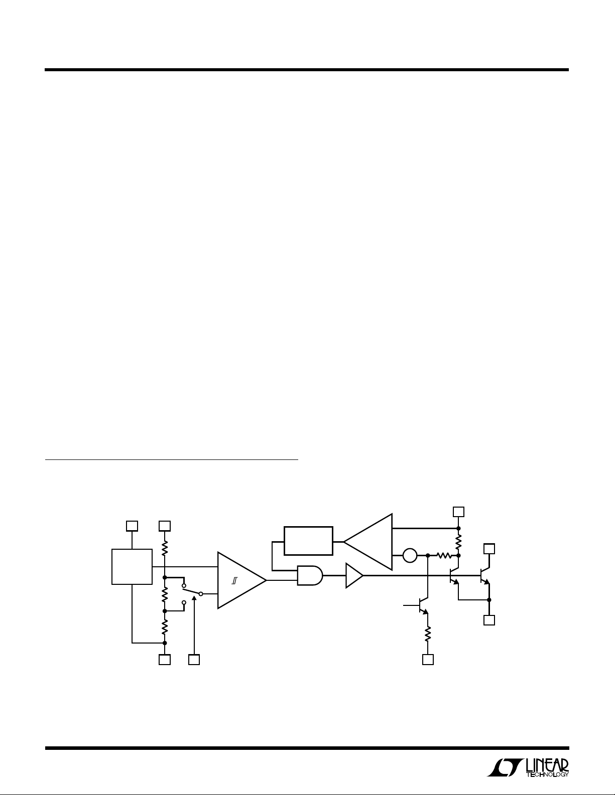
Theory of Operation
Figure 1 is a block diagram of the LT1300/LT1301. Refer
also to Figure 2 for associated component hookup. When
A1’s negative input, related to the SENSE pin voltage by the
appropriate resistor-divider ratio, is higher than the 1.25V
reference voltage, A1’s output is low. A2, A3 and the
oscillator are turned off, drawing no current. Only the
reference and A1 consume current, typically 120µ A. When
the voltage at A1’s negative input decreases below 1.25V,
overcoming A1’s 6mV hysteresis, A1’s output goes high,
enabling the oscillator, current comparator A2, and driver
A3. Quiescent current increases to 2mA as the device
prepares for high current switching. Q1 then turns on in a
controlled saturation for (nominally) 5.3µ s or until current
comparator A2 trips, whichever comes first. After a fixed
off-time of (nominally) 1.2µ s, Q1 turns on again. Refering
to Figure 2, the LT1300’s switching causes current to
alternately build up in L1 and dump into output capacitor
C1via D1, increasing the output voltage. When the output
is high enough to cause A1’s output to go low (Figure 1),
switching action ceases. C1 is left to supply current to the
Burst ModeTM is a trademark of Linear Technology Corporation
SENSESHUTDOWN
500k
1.25V
REFERENCE
144k
161k
GND SELECT
CURRENT
COMPARATOR
OSCILLATOR
5.3µs ON
1.2µs OFF
+
A3
DRIVER
–
A1
SLOW
COMPARATOR
ENABLE
Figure 1. LT1300/LT1301 Block Diagram
A2
V
IN
+
R1
SW
3Ω
Q2
3×
PGND
AN59 • F01
Q1
500×
–
BIAS
+
–
18mV
R2
700Ω
Q3
8.5k
I
LIM
AN59-2
Application Note 59
load until V
decreases enough to force A1’s output
OUT
high, and the entire cycle repeats. If switch current reaches
1A, causing A2 to trip, switch on-time is reduced and offtime increases slightly. This allows continuous mode
operation during bursts. Current comparator A2 monitors
the voltage across 3Ω resistor R1 which is
directly related
to inductor L1’s current. Q2’s collector current is set by
the emitter-area ratio to 0.6% of Q1’s collector current.
When R1’s voltage drop exceeds 18mV, corresponding to
1A inductor current, A2’s output goes high, truncating the
on-time portion of the oscillator cycle and increasing offtime to about 2µs as shown in Figure 3, trace A. This
programmed peak current can be reduced by tying the
I
pin to ground, causing 15µA to flow through R2 into
LIM
Q3’s collector. Q3’s current causes a 10.4mV drop in R2,
so that only an additional 7.6mV is required across R1 to
turn off the switch. This corresponds to a 400mA switch
current, as shown in Figure 3, trace B. The reduced peak
L1*
10µH
Burst ModeTM Operation
Burst ModeTM operation, a technique used by many LTC
switching regulator products, extends high efficiency
over widely varying loads.
At light load, switching regulators employing traditional
PWM regulation techniques suffer from low efficiency.
This is primarily due to relatively high quiescent (or
housekeeping) supply current and AC switching losses
resulting from constant frequency operation.
100
Burst ModeTM
SWITCHER
75
NON-Burst Mode
50
EFFICIENCY (%)
25
TM
2×
AA
CELL
SHUTDOWN
+
100µF
*SUMIDA CD54-100LC
COILCRAFT D03316-103
NC
SELECT
SHDN
I
LIM
V
IN
LT1300
SENSE
GND PGND
SW
D1
1N5817
+
Figure 2. Two-Cell to 5V DC/DC Converter Delivers >200mA
with a 2V Input
TRACE A
500mA/DIV
I
PIN
LIM
OPEN
TRACE B
500mA/DIV
I
PIN
LIM
GROUNDED
5µs/DIV
Figure 3. Switch Pin Current with I
Floating or Grounded
LIM
AN59 • F03
C1
100µF
AN59 • F02
5V OUTPUT
200mA
0
1255075
POWER (%)
100
AN59 • F1a
Figure 1a. Characteristics of Burst and Non-Burst Switchers
As seen in Figure 1a, the switching regulator not using
Burst ModeTM operation does not reach peak efficiency
until load power approaches 100%. Relatively high
fixed power drain inside the regulator accounts for the
efficiency fall-off as load is decreased. The regulator
utilizing Burst ModeTM operation, on the other hand,
maintains its high efficiency at light loads. It does this
by delivering energy to the output in discrete peak
efficiency packets. The energy packets result in a small
amount of ripple voltage (typically 50mV) on the output.
When not delivering these packets of energy to the
output, the regulator puts itself in a “sleep” mode with
only a voltage reference and a comparator powered up.
These two functions can be accomplished with very low
power drain. As the load is decreased to zero, even the
small amount of power consumed in sleep mode becomes significant compared to the load, resulting ultimately in decreasing efficiency.
AN59-3
Application Note 59
BATTERY
TIME (HOURS)
0
0
OUTPUT/BATTERY VOLTAGE (V)
5.0
11
AN59 • F06
9651
1.0
2.0
4.5
4.0
3.5
3.0
2.5
1.5
0.5
234 78 10
2× L91
LITHIUM
2× E91
ALKALINE
OUTPUT
switch current reduces I2R losses in Q1, L1, C1, and D1.
You can increase efficiency by doing this provided that the
accompaning reduction in full load output current is acceptable. Lower peak currents also extend alkaline battery
life due to the alkaline cells’ high internal impedance.
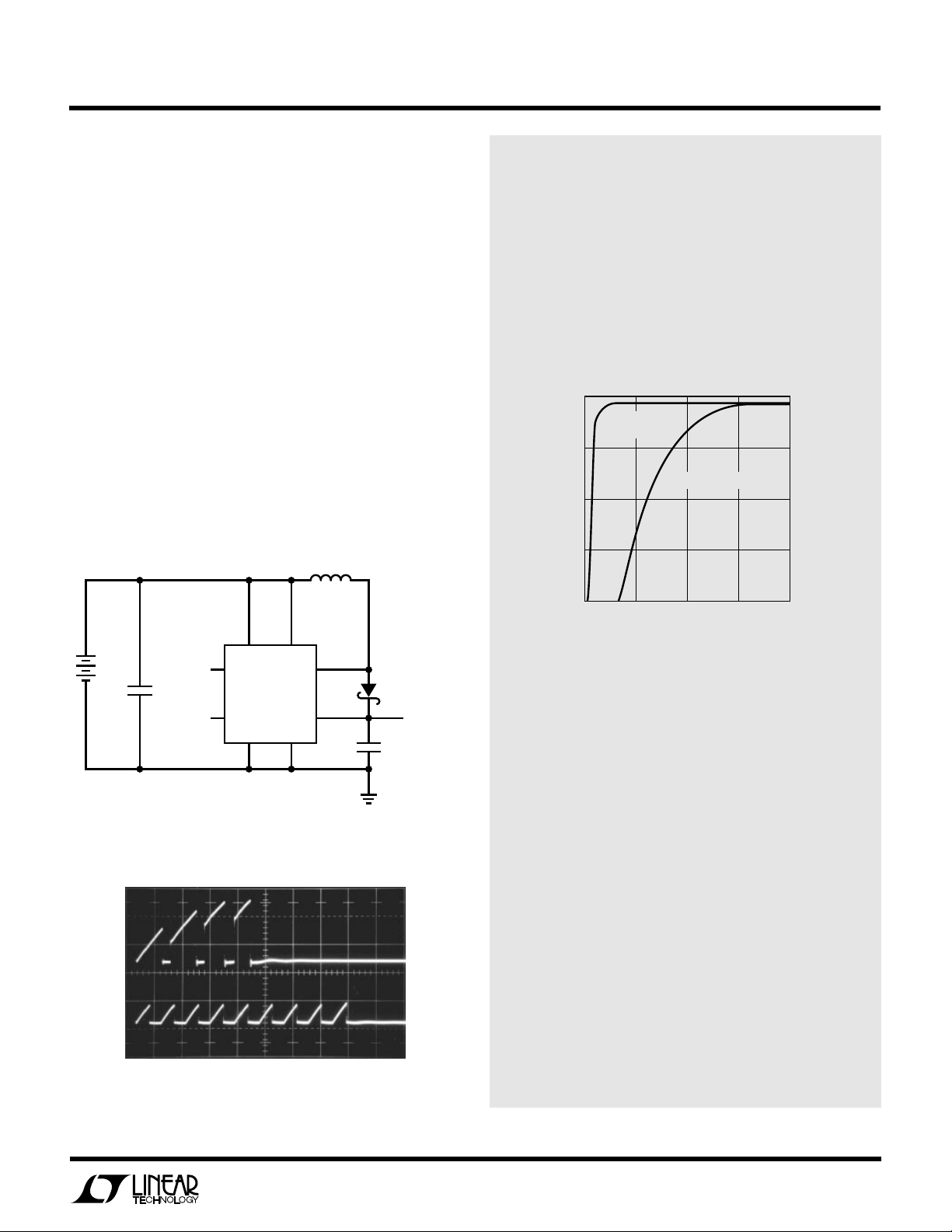
5V from 2 Cells
Figure 2’s circuit provides 5V from a 2-cell input. Shutdown is effected by taking the SHUTDOWN pin high. V
IN
current drops to 10µ A in this condition. This simple boost
topology does not provide output isolation and in shutdown the load is still connected to the battery via L1 and
D1. Figure 4 shows the efficiency of the circuit with a range
of input voltages, including a fresh battery (3V) and an
“almost dead” battery (2V). At load currents below a few
milliamperes, the 120µA quiescent current of the device
becomes significant, causing the fall-off in efficiency de-
90
88
86
84
82
80
EFFICIENCY (%)
78
76
74
1
10 500
LOAD CURRENT (mA)
VIN = 4.0V
VIN = 3.0V
VIN = 2.5V
VIN = 2.0V
100
AN59 • F04
tailed in Figure 4. At load currents in the 20mA to 200mA
range, efficiency flattens out in the 80% to 88% range,
depending on the input. Figure 5 details circuit operation.
V
is shown in trace A. The burst repetition pattern is
OUT
clearly shown as V
decays, then steps back up due to
OUT
switching action. Trace B shows the voltage at the switch
node. The damped, high frequency waveform at the end of
each burst is due to the inductor “ringing off,” forming an
LC tank with the switch and diode capacitance. It is not
harmful and contains far less energy than the high speed
edge which occurs when the switch turns off. Switch
current is shown in trace C. The current comparator inside
the LT1300 controls peak switch current, turning off the
switch when the current reaches approximately 1A.
Although efficiency curves present useful information, a
more important measure of battery-powered DC/DC converter performance is operating life. Figures 6 and 7 detail
battery life tests with Figure 2’s circuit at load currents of
100mA and 200mA respectively. Operating life curves are
shown using both Eveready E91 alkaline cells and new L91
“Hi-Energy” lithium cells. These lithium cells, new to the
market, are specifically designed for high drain applications. The performance advantage of lithium is about 2:1
at 100mA load current (Figure 6), increasing to 2.5:1 at
200mA load (Figure 7). Alkaline cells perform poorly at
high drain rates because their internal impedance ranges
V
OUT
A = 20mV/DIV
AC COUPLED
V
SW
B = 5V/DIV
AN59-4
I
SW
C = 1A/DIV
Figure 4. Efficiency of Figure 2’s Circuit
20µs/DIV
Figure 5. Burst ModeTM Operation in Action
AN59 • F05
Figure 6. Two Eveready L91 Lithium AA Cells Provide
Approximately Twice the Life of E91 AA Alkaline Cells at a
100mA Load Current

Application Note 59
TIME (HOURS)
0
0
OUTPUT/BATTERY VOLTAGE (V)
5.0
22
AN59 • F10
1812102
1.0
2.0
4.5
4.0
3.5
3.0
2.5
1.5
0.5
468 1416 20
2× L91
LITHIUM
2× E91
ALKALINE
OUTPUT
BATTERY
24
5.0
OUTPUT
4.5
4.0
3.5
3.0
2.5
2.0
1.5
1.0
OUTPUT/BATTERY VOLTAGE (V)
0.5
0
0
1.0 1.5 2.0 3.5 4.0 5.0
2× E91
ALKALINE
2× L91
LITHIUM
BATTERY
TIME (HOURS)
5.5
4.53.02.50.5
AN59 • F07
Figure 7. Doubling Load Current to 200mA Causes E91 Alkaline
Battery Life to Drop by 2/3; L91 Lithium Battery Shows 2.5:1
Difference in Operating Life
from 0.20Ω to 0.50Ω, causing a large voltage drop within
the cell. The alkaline cells feel quite warm at 200mA load
current, the result of I2R losses inside the cells.
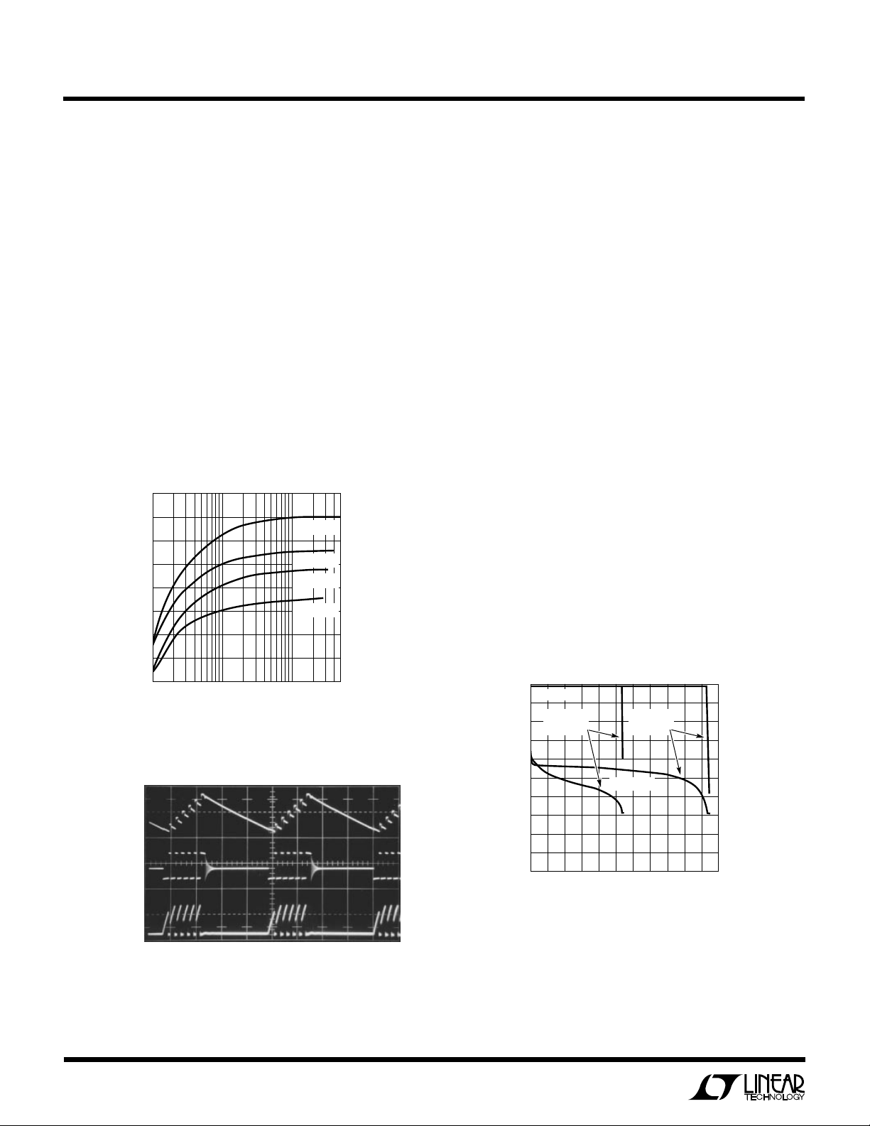
The reduced power circuit shown in Figure 8 can generate 5V at currents up to 50mA. Here the I
LIM
pin is
grounded, reducing peak switch current to 400mA.
Lower profile components can be used in this circuit.
The capacitors are C-case size solid tantalum and inductor L1 is the tallest component at 3.2mm. The reduced
peak current also extends battery life since the I2R loss
due to internal battery impedance is reduced. Figure 9
L1*
22µH
90
88
86
84
82
80
EFFICIENCY (%)
78
76
74
1
10 100
LOAD CURRENT (mA)
VIN = 3V
VIN = 2.5V
VIN = 2V
AN59 • F09
Figure 9. Efficiency of Figure 8’s Circuit
Figure 10. 50mA Load and Reduced Switch Current Are
Kind to E91 AA Alkaline Battery; the Advantages of L91
Lithium Are Not as Evident
2×
AA
CELL
+
*COILCRAFT 1608-223
Figure 8. Lower Power Applications Can Use Smaller
Components. L1 is Tallest Component at 3.1mm
SHUTDOWN
47µF
SELECT
SHDN
LT1300
I
LIM
GND PGND
V
IN
SW
SENSE
details efficiency versus load current for several input
voltages and Figure 10 shows battery life at a 50mA load.
Note that the L91 lithium battery lasts only about 40%
longer than the alkaline. The higher cost of the lithium
cells makes the alkaline cells more cost effective in this
application. A pair of Eveready AAA alkaline cells (type
E92) lasts 96.6 hours with 5mA load, very close to the
+
D1
MBRS140T3
5V OUTPUT
50mA
33µF
rated capacity of the battery.
AN59 • F08
AN59-5

Application Note 59
A 4-Cell Application
A 4-cell pack is a convenient, popular battery size. Alkaline
cells are sold in 4-packs at retail stores and four cells
usually provide sufficient energy to keep battery replacement frequency reasonable. Generating 5V from four
cells, however, is a bit tricky. A fresh 4-cell pack has a
terminal voltage of 6.4V but at the end of its life, the pack’s
terminal voltage is around 3.2V; hence, the DC/DC converter must step the voltage either up or down, depending
on the state of the batteries.
A flyback topology with a costly, custom designed transformer could be employed, but Figure 11’s circuit gets
around these problems by using a flying capacitor scheme
along with a second inductor. The circuit also isolates the
input from the output, allowing the output to go to 0V
during shutdown. The circuit can be divided conceptually
into boost and buck sections. L1 and the LT1300 switch
comprise the boost or step-up section, and L2, D1, and C3
comprise the buck or step-down section. C2 is charged to
VIN and acts as a level shift between the two sections. The
switch node toggles between ground and VIN + V
the L2-C2 diode node toggles between –VIN and V
OUT
, and
OUT
+
VD. Figure 12 shows efficiency versus load current for the
circuit. All four energy storage elements must handle
power, which accounts for the lower efficiency of this
circuit compared to the simpler boost circuit in Figure 2.
84
82
80
78
76
74
72
EFFICIENCY (%)
70
68
66
64
1
VIN = 3V
VIN = 4V
VIN = 5V
VIN = 6V
10
LOAD CURRENT (mA)
100
AN59 • F12
Figure 12. Efficiency of Up-Down Converter in Figure 11
Efficiency is directly related to the ESR and DCR of the
capacitors and inductors used. Better capacitors cost
more money. Better inductors do not necessarily cost
more, but they do take up more space. Worst case RMS
current through C2 occurs at minimum input voltage and
measures 0.4A at full load with a 3V input. C2’s specified
maximum RMS current must be greater than this worst
case current. The Sanyo capacitors noted specify a maximum ESR of 0.045Ω with a maximum ripple current rating
of 2.1A. The Gowanda inductors specify a maximum DCR
of 0.058Ω.
AN59-6
C2**
100µF
+
L2*
27µH
C3**
100µF
1N5817
5V OR
3.3V
220mA
+
AN59 • F11
NC
4×
AA
+
CELLS
*L1, L2 = GOWANDA GA20-272K (716) 532-2234
**C1, C2, C3 = SANYO OS-CON 16SA100M (619) 661-6835
5V/3.3V
C1**
100µF
SHUTDOWN
I
LIM
SELECT
GND PGND
LT1300
V
IN
SW
SENSESHDN
L1*
27µH
Figure 11. 4-Cell to 3.3V or 5V Converter Output Goes to Zero When in Shutdown.
Inductors May Have, But Do Not Require Coupling; a Transformer or Two Separate
Units Can Be Used

Application Note 59
LT1301 Outputs 5V or 12V
The LT1301 is identical to the LT1300 in every way except
output voltage. The LT1301 can be set to a 5V or 12V
output via its SELECT pin. Figure 13 shows a simple 3.3V
or 5V to 12V step-up converter. It can generate 120mA at
12V from either 3.3V or 5V inputs, enabling the circuit to
provide VPP on a PCMCIA card socket. Figure 14 shows
the circuit’s efficiency. Switch voltage drop is a smaller
percentage of input voltage at 5V than 3.3V, resulting in a
high efficiency at 5V input.
L1*
3.3V
OR 5V
INPUT
SELECT
SHUTDOWN
+
*L1 =
100µF
SUMIDA
CD75-220K
(708) 956-0666
SHDN
LT1301
I
LIM
GND PGND
SENSE
Figure 13. LT1301 Delivers 12V from 3.3V or 5V Input
90
88
86
84
82
80
EFFICIENCY (%)
78
76
74
VIN = 5V
VIN = 3.3V
1
10 100
LOAD CURRENT (mA)
Figure 14. Efficiency of Figure 13’s Circuit
22µH
V
IN
SW
1N5817
12V
OUTPUT
+
47µF0.1µF
AN59 • F13
AN59 • F14
THE LT1300: TWO CELLS TO REAL WORLD INTERFACE
By Dale Eagar
Introduction
The LT1300 micropower, high speed, step-up DC/DC
converter opens up many new applications to the user,
such as those requiring high efficiency in battery-operated
equipment. The LT1300 can be used to produce high
voltages for many specialized tasks with high efficiency.
Here are three such applications. In the first application, a
flame detector, the LT1300 is used to produce 325V
DC
while drawing a mere 200µA from two C-size cells.
Flame Sensor
An interesting characteristic of flame is that it emits short
wavelength ultraviolet light (<260nm). This short wavelength light falls into a window of the light spectrum that
is relatively empty. Tungsten light, fluorescent light and
sunlight below the atmosphere are almost totally devoid of
spectral energy in this window. The circuit shown in
Figure 15 uses a photoelectric sensor with a sufficiently
high cathode work function to make it blind to anything
with a wavelength longer than 260nm (such as normal UV,
visible light or infrared). Cathode work function is a
measure of how hard it is to free an electron from an atom;
when related to light illuminating a cathode, it specifies the
minimum energy of a photon that can liberate an electron.
UV photons have higher energy than visible light.
Theory of Operation (see Figure 15)
The LT1300 and transformer T1 form a flyback converter
to step up the voltage from 3V to 325V. The secondary
winding of T1 connects through D1 (a MUR1100) to C1, a
holding capacitor for the 325VDC, which in turn is applied
to the anode of the photoelectric sensor tube V1. The
LT1300 SENSE pin senses the voltage on C1, as scaled by
the turns ratio, through T1. The voltage on the primary
winding is programmed to be 10.6V, translating to 325V
on C1. When C1 has charged to 325V the feedback loop
comprised of D3, R2 and Q1 kicks in and charges C4
through D4. When the voltage at C4 exceeds 3.3V the
LT1300 goes into its wait mode. In wait mode the LT1300
AN59-7

Application Note 59
D1
MUR1100
T1
C1
V1
R2868
1N4148
PULSE
R1
100k
V1 =
HAMAMATSU R2868
FLAME SENSOR
HAMAMATSU (408) 261-2022
=
T1
COILTRONICS CTX02-12186
COILTRONICS (407) 241-7876
=
Q1
ZETEX ZTX788
ZETEX (516) 543-7100
=
C1
47pF > 500V
D2
47pF
3V
3V
V
3
SHUTDOWN
C2
0.01µF
54
NC
U1
LT1300
I
LIM
SEL GND
218
Figure 15. Flame Detector
consumes only 120µA of current. The LT1300 stays in
wait mode until the voltage on C4 falls below 3.3V at which
time the LT1300 turns on to burst recharge both C1 and
C4. Burst Mode operation ensures 30Hz oscillation in this
system. This rate is determined by the value of C4, the
internal sense resistance to ground in the LT1300 (approximately 1MΩ), and the amount of overcharge C4 gets
when charging. D5 is a Schottky catch diode to keep
reverse current out of U1.
When illuminated with a photon of sufficient energy the
photoelectric tube’s cathode liberates an electron. The
tube V1 has 325V across its terminals to get sufficient
energy into a liberated photo-electron to ionize the gas
that fills the tube. Once the gas in the tube ionizes there are
more electrons available; they cause a chain reaction in
the tube that causes the tube to avalanche. When the tube
avalanches most of the charge on C1 is transferred to C2
and the voltage across C1 drops to a fraction of its original
325V. When C2 has charged to 3.6V all the excess charge
residing in C1 gets bypassed through D2 back into the
battery. The voltage across C2 is the output signal called
PULSE. PULSE asserts the shutdown pin of the LT1300,
allowing the plasma in the photoelectric tube to quench.
IN
6
D5
1N5718
C3
+
100µF
6.3V
7
SW
SENSE
PGND
ZTX788
Q1
D4
1N5718
C4
0.47µF
R2
1k
D3
1N758A
3V
AN59 • F15
For you analog purists, page 8 of the October 1993 issue
of
Linear Technology
magazine shows a discriminator
circuit with low-battery detect for a complete 3V flame
alarm. The discriminator is needed because the photo
detector occasionally detects a cosmic ray or some rare
room light photon.
Infinite Input Impedance Voltage Buffer
In the flame detector circuit (Figure 15), it is difficult to
measure the voltage across C1 because almost any load
invalidates the meter reading. This next application for the
LT1300 is a voltage buffer that overcomes this measurement problem. This is a four-terminal, unity-gain buffer as
shown functionally in Figure 16. The input impedance is
+OUT
–
ISOLATION
+IN
–IN
+
Figure 16. Voltage Buffer Block Diagram
+
E
AN59 • F16
–OUT
AN59-8

Application Note 59
+OUT
+IN
SW1
1.5V
1.5V
R1, R10 =
3V
LT1097
R3
1M
C1
1000pF
R1
100M
T1 =
R2
1M
COILTRONICS CTX02-12179
COILTRONICS (407) 241-7876
VICTOREEN SLIM-MOX100
VICTOREEN (216) 248-9300
R10
0.01µF
2
3
–OUT
C8
0.1
C2
–
LT1097
+
100M
+
R4
100k
U1
–IN
3V
R11
20Ω
7
U1
4
C7
1000pF
C6
100µF
6.3V
57
NC
I
4
SENSE
10k
6
6
V
IN
LIM
U2
LT1300
218
R5
R6
10k
D3
MUR1110
R9
5.1Ω
SW
3
SHUT-
DOWN
R7
1k
Q1
2N3904
3V
100µF
6.3V
C5
Z1
15V
C3
0.01µF
D1
1N4148
R8
1M
T1
+
C4
220pF
D2
1N4148
3V
AN59 • F17
Figure 17. Voltage Buffer Schematic
essentially infinite, the input bias current is negligible and
the input offset voltage is less than 0.05V. The output
voltage tracks the input voltage from 0V to 520V. For
safety (and to isolate the input capacitance) a 100M
resistor is placed in series with the input, but with the
± 570pA of input bias current (over temperature) for the
LT1097, this translates into only ±57mV of additional
offset. The input impedance of this buffer measures four
trillion ohms when measured with a 100V to 400V input.
The detailed circuit is shown in Figure 17.
Theory of Operation
U1 monitors the voltage difference between the circuit’s
noninverting input and output and attempts to make it
zero. If the voltage on the noninverting input is less than
the voltage on the noninverting output, U1’s output goes
positive, turning Q1 on slightly. Q1 acts as a current sink
discharging C3. When the voltage on C3 falls below
approximately 0.6V, U2 is enabled. When it is enabled U2
turns its switch on (U2’s pin 7 pulls low, to near 0V). This
causes approximately 3V to be imposed across the primary winding of T1. The magnetizing inductance of the
primary winding of T1, across which a voltage is applied,
requires a steadily increasing current. At the same time,
C4 is charged through D2. When the current flowing
through the switch of the LT1300 reaches 1A, the LT1300
switches off. The magnetizing inductance of the primary
winding of T1, seeing that the LT1300 is attempting to
discontinue current flow, takes over by swinging positive
in voltage until it finds something that will take the 1A of
magnetizing current. While the primary winding is finding
somewhere to put the magnetizing current, the secondary
winding takes it upon itself to do the same, but due to its
turns ratio with the primary winding, it moves 100 times
faster and 100 times as far as the primary winding. T1’s
secondary dumps a significant portion of the magnetizing
energy into C7 via D3, thus forming a flyback inverter.
AN59-9

Application Note 59
AN59 •F18
V
IN
SHUTDOWN
SW
I
LIM
SENSE
SEL GND
PGND
U1
LT1300
218
54
7
NC
3
6
PWM
IN
C1
100µF
6.3V
3V
CCFL LAMP =
T1
=
C2
=
JKL BF650-20B
JKL (800) 897-3056
COILTRONICS CTX02-12189
COILTRONICS (407) 241-7876
15pF, 500V
T1
+
D1
1N5718
C2
15pF
CCFL
Z1 dissipates the energy stored in T1’s leakage inductance. During the flyback time, C4 charges C3 through D1.
This causes the voltage across C3 to exceed 0.6V, shutting
down U2. U2 stays shut down until Q1 discharges C3 to
restart the sequence.
When the +output voltage is more positive than the + input
voltage the output of U1 goes low, Q1 stays off, R8 keeps
C3 charged to more than 0.6V, and U2 stays shut down.
The parallel combination of R10 and the load resistance
(e.g., 10M in a handheld voltmeter) discharges C7 and the
+output and the +input voltages are again equal. The
current output of this circuit is limited to a safe value (1mA
at 50V, 0.1mA at 500V) even when the +input is attached
to 500V. We do not recommend increasing the value of C7
because at higher voltages it may become a shock hazard.
Battery life is 40 hours for a pair of AA alkaline batteries
driving 10MΩ at 500V.
Cold Cathode Florescent Lamp Driver
CCFLs seem to be the latest craze; they offer high brightness, long life, small size and produce white light. Figure
18 shows a CCFL driver circuit.
Electronic Light Stick
Camping in November with my kids has its own unique
problems, even if we aren’t camping in six feet of snow.
Although we had the usual light sources something was
missing, namely a light that simulates the natural sunset
at bedtime to wind the kids down for the night. The circuit
in Figures 18 and 19 (see explantation below) details a
high efficiency fluorescent lantern with a built-in sunset
feature.
The function of the circuit is as follows:
• To turn on: switch SW1 into the ON position.
• To turn off fast: switch SW1 into the OFF position.
• To simulate sunset:
1. Turn light ON.
2. Switch SW1 into the SUNSET position.
This application uses the circuitry of both Figure 18 and
Figure 19. The pulse-width output of Figure 19 drives the
pulse-width input of Figure 18.
Theory of Operation
This is a forward/flyback inverter optimized for minimum
parts count. When enabled, U1 charges the primary winding of T1 to 1A, and lets go. T1 then flies back exciting
many hundreds of volts across its secondary winding,
which in turn ionizes the CCFL. Because the initial current
through the CCFL is only in one direction, C2 takes on a DC
potential. As the circuit runs, the voltage across C2 stabilizes at about 100VDC. Additionally, C2 removes the DC
current component from the tube, extending tube life. The
nonlinear V/I characteristic of the CCFL, in conjunction
with C2, forces the converter to run in both forward and
flyback modes simultaneously. The light intensity can be
pulse-width modulated by modulating the shutdown pin.
When the shutdown pin is pulled high the LT1300 goes
into its shutdown mode where it draws only 10µ A of input
current.
Figure 18. CCFL Driver
AN59-10

Application Note 59
1N4148
SUNSET
10Ω
LT1178
D1
OFF
ON
R7
3V
3V
C4
0.1µF
LIGHT LEVEL
PROGRAM
R7
100M
R5
1k
C2
470µF
0.022µF
D2
2N3904
R1
300k
R6
1M
PULSE-
7
WIDTH
OUT
C3
0.01µF
6
–
+
C1
LT1178
5
+
SAWTOOTH
U1B
lated. When the voltage on C2 is at or below 1V the light is
off. D1 and R5 charge and hold C2 when SW1 is in the ON
position. R5 and SW1 discharge and hold C2 when SW1
is in the OFF position. The combination of D2, R6 and U1B
discharge C2 when SW1 is in the SUNSET position. The
discharging of C2 when in the SUNSET mode is doubly
exponential causing the tail end of the simulated sunset to
go very slowly (a good idea because kids have a logarithmic response to light). The first exponential aspect of the
SUNSET decay is implemented by R6 and C2 which form
an exponential RC time constant. The second exponential
aspect of the SUNSET decay is implemented because R6
8
4
270k
3V
2
–
U1A
LT1178
3
+
R3
R4
200k
270k
1
R2
AN59 • F19
is driven by U1B pin 7, whose duty factor is changing,
causing the off-time to decrease exponentially as the light
level fades. The output of U1B is a pulse-width modulated
level gating the light driver on and off. The lamp is
illuminated when U1B’s output is low. C3 is a trash
compactor and R7 and C4 form a trash compactor to
decouple U1 from the high frequency ripple generated by
the switcher.
Figure 19. Electronic Light Stick Controller for the CCFL Driver
Circuit Shown in Figure 18. This Controller, When Controlling the
CCFL, Causes the Light Output Level to Fade from Full Brightness
to Off, Thus Simulating a Natural Sunset.
U1A, R1 to R4 and C1 form a sawtooth oscillator for pulsewidth modulating the light (implementing light levels less
than 100%). U1B acts as a comparator, comparing the
sawtooth output of the oscillator with the programmed
light level (as seen on the +terminal of C2). C2 is the
holding capacitor that programs the light level; when it is
charged to 2.5V the light is on 100% of the time. As the
voltage on C2 drops below 2.5V, the overall light level
decreases because the light is being pulse-width modu-
1.8V TO 10V
C1
+
H = LEDs OFF
L = LEDs ON
PWM = ADJUSTABLE
LIGHT LEVEL
47µF
16V
5
3
6
V
CC
I
LIM
SHDN
182
LT1300
DGND
SW
SELGND
22µH
7
4
FB
Constant Current Source
The LT1300 can be configured as a constant current
source, a current source that not only possesses good
power conversion efficiency, but can be shut down to a
state of practically no current draw. These benefits coupled
with the LT1300’s ability to operate over a wide input
voltage range, make the LT1300 an ideal candidate for
many current operated devices. Popular uses include
solenoid drivers, relay drivers, small motor drives and LED
drivers.
Here is an example of a high efficiency LED driver. The LED
light source (shown in Figure 20) is used in applications
1N5817
+
C2
I
LED
10µF
0.8
=
R2
R1
100k
LT1004-2.5
AN59 • F20
8 ×
•
•
1.6V LEDs
C3
1µF
R2
39Ω
Figure 20. Backlight LED Driver
Information furnished by Linear Technology Corporation is believed to be accurate and reliable. However,
no responsibility is assumed for its use. Linear Technology Corporation makes no representation that
the interconnection of its circuits as described herein will not infringe on existing patent rights.
AN59-11

Application Note 59
89
88
87
86
85
84
EFFICIENCY (%)
83
82
81
80
123
4
610
5
INPUT VOLTAGE (V)
789
AN59 • F21
Figure 21. Efficiency of LED Driver
ranging from LCD backlights to special flashlights that
preserve full night vision. This circuit sports an impressive
list of features:
• Logic input to strobe LED’s on/off
• Low current draw when off (10µA)
• Constant LED drive current when on (20mA)
Theory of Operation
When enabled the LT1300 runs in Burst ModeTM, regulating the voltage on the FB pin to 3.3V. Subtracting 2.5V
(corresponding to the knee voltage of the LT1004-2.5)
from the 3.3V voltage at the FB pin yields 0.8V, which is
seen across R2. This 0.8V and the value of R2 sets the
output current level through the LEDs. For proper functionality the voltage across the LED stack should be:
1. Greater than the maximum input voltage less one
Schottky drop.
2. Less than 14V.
The LT1300 is optimized for battery operation and lends
itself to these and many more applications.
• LED current unaffected by temperature
• LED current constant with input voltage range
(1.8V to 10V)
• High overall efficiency (87%)
• Small size
AN59-12
Linear Technology Corporation
1630 McCarthy Blvd., Milpitas, CA 95035-7487
(408) 432-1900
●
FAX
: (408) 434-0507
●
TELEX
: 499-3977
LT/GP 0294 10K • PRINTED IN USA
LINEAR TECHNOLOGY CORPORATION 1994
 Loading...