

Linear Technology LT1301 Datasheet
FEATURES
LOAD CURRENT (mA)
10 100 300
LT1301 TA2
1
0
72
74
EFFICIENCY (%)
76
78
80
82
90
84
86
88
VIN = 5V
VIN = 3.3V
■
12V at 120mA from 5V or 3.3V Supply
■
Supply Voltage as Low as 1.8V
■
Better High Current Efficiency Than CMOS
■
Up to 89% Efficiency
■
120µA Quiescent Current
■
Shutdown to 10µA
■
Programmable 5V or 12V Output
■
Low V
■
I
Pin Programs Peak Switch Current
LIM
■
Uses Inexpensive Surface Mount Inductors
■
8-Lead DIP or SOIC Package
Switch: 170mV at 1A Typical
CESAT
U
APPLICATIONS
■
Flash Memory VPP Generator
■
Palmtop Computers
■
Portable Instruments
■
Bar-Code Scanners
■
Personal Digital Assistants
■
PCMCIA Cards
LT1301
Micropower High Efficiency
5V/12V Step-Up DC/DC
Converter for Flash Memory
U
DESCRIPTION
The LT1301 is a micropower step-up DC/DC converter that
utilizes Burst Mode™ operation. The device can deliver 5V
or 12V from a two-cell battery input. It features programmable 5V or 12V output via a logic-controlled input, noload quiescent current of 120µ A and a shutdown pin which
reduces supply current to 10µ A. The on-chip power switch
has a low 170mV saturation voltage at a switch current of
1A, a four-fold reduction over prior designs. A 155kHz
internal oscillator allows the use of extremely small surface mount inductors and capacitors. Operation is guaranteed at 1.8V input. This allows more energy to be extracted
from the battery, increasing operating life. The I
be used for soft start or to program peak switch current
with a single resistor allowing the use of even smaller
inductors in lighter load applications. The LT1301 is
available in an 8-lead SOIC package, minimizing board
space requirements. For a selectable 3.3V/5V step-up
converter, please see the LT1300. For higher output
power, see the LT1302.
Burst Mode is a trademark of Linear Technology Corporation.
LIM
pin can
3.3V
U
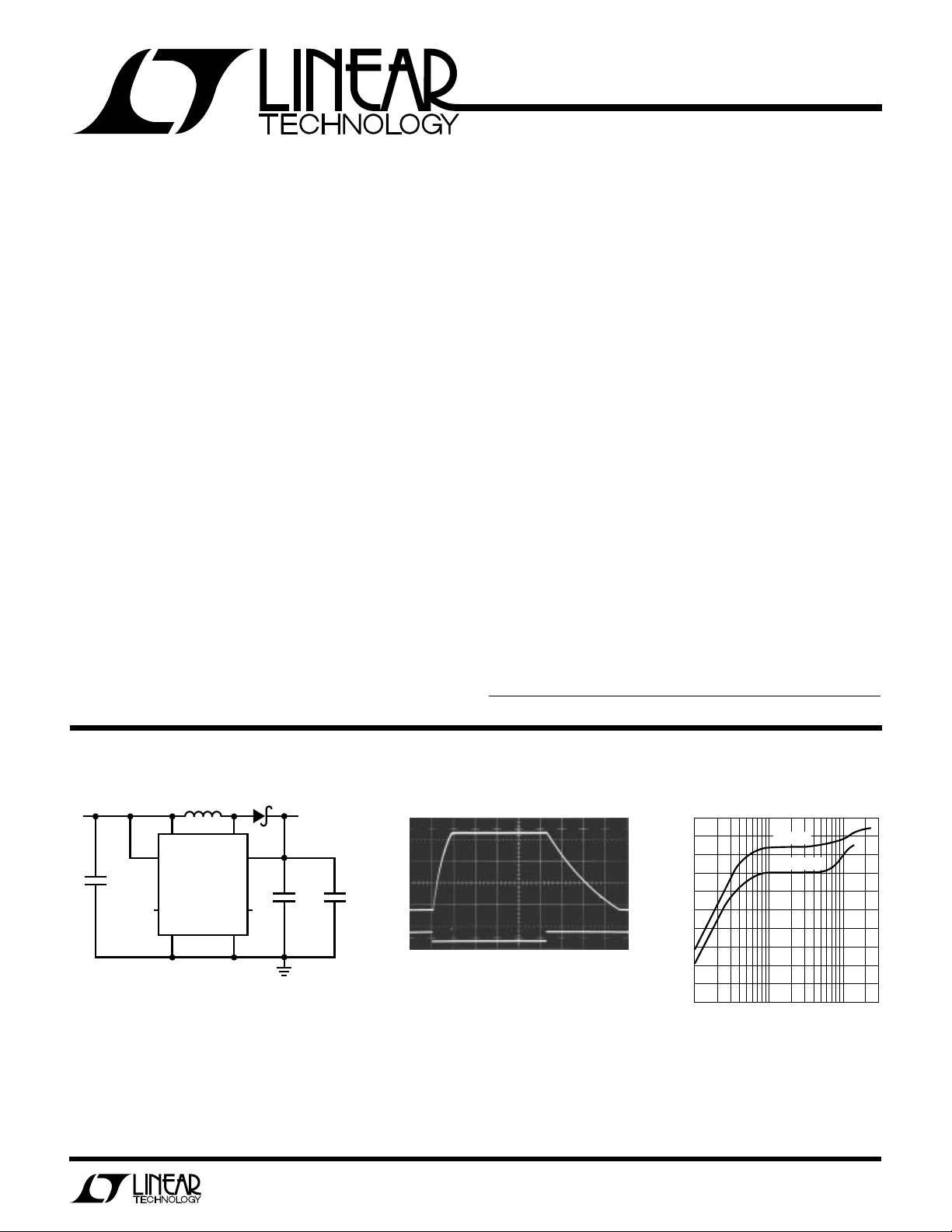
TYPICAL APPLICATIONS N
L1
V
IN
SELECT
SHDN
PGND
33µH
LT1301
5V
OR
+
C1
47µF
SHUTDOWN
*REQUIRED FOR 5V OUTPUT
L1 = COILCRAFT DO3316-333
OR SUMIDA CD73-330KC
D1 = 1N5817 OR MOTOROLA
MBRS130LT3
C1 = AVX TPSD476M016R0100
OR SANYO OS-CON 165A47M
C2 = AVX TPSD336M020R0100
OR SANYO OS-CON 205A33M
Figure 1. 3.3V/5V to 12V Step-Up Converter
SW
SENSE
I
LIM
GND
D1
N/C
+
12V
OUTPUT
C2
33µF
20V
LT1301 F1
0.1µF*
12V
V
OUT
2V/DIV
SHUTDOWN
10V/DIV
V
= 5V, V
IN
LOAD = 100Ω
Output Voltage
1ms/DIV
= 12V
OUT
Efficiency
LT1301 TAO1
LT1300 F2
1
LT1301
WW
W
ABSOLUTE MAXIMUM RATINGS
VIN Voltage .............................................................. 10V
SW1 Voltage ............................................................ 20V
Sense Voltage .......................................................... 20V
Shutdown Voltage ................................................... 10V
Select Voltage .......................................................... 10V
I
Voltage ............................................................ 0.5V
LIM
Maximum Power Dissipation ............................. 500mW
Operating Temperature Range
LT1301C................................................... 0°C to 70°C
LT1301I .................................................. 40°C to 85°C
U
U
W
PACKAGE/ORDER INFORMATION
TOP VIEW
GND
1
SEL
2
SHDN
3
SENSE
4
N8 PACKAGE
8-LEAD PLASTIC DIP
T
= 100°C, θJA = 150°C/W
JMAX
PGND
8
SW
7
V
6
IN
I
5
LIM
S8 PACKAGE
8-LEAD PLASTIC SOIC
ORDER PART
NUMBER
LT1301CN8
LT1301CS8
LT1301IS8
S8 PART MARKING
1301
1301I
U
Storage Temperature Range ................. –65°C to 150°C
Lead Temperature (Soldering, 10 sec)..................300°C
ELECTRICAL CHARACTERISTICS
SYMBOL PARAMETER CONDITIONS MIN TYP MAX UNITS
I
Q
VINInput Voltage Range 1.8 V
V
OUT
DC Maximum Duty Cycle 75 86 95 %
t
ON
V
CESAT
V
SHDNH
V
SHDNL
V
SELH
V
SELL
I
SHDN
I
SEL
The ● denotes specifications which apply over the 0°C to 70°C
temperature range.
Quiescent Current V
Output Sense Voltage V
Output Referred V
Comparator Hysteresis V
Oscillator Frequency Current Limit not Asserted. 120 155 185 kHz
Oscillator TC 0.2 %/°C
Switch On-Time Current Limit not Asserted. 5.6 µs
Output Line Regulation 1.8V < VIN < 6V ● 0.06 0.15 %/V
Switch Saturation Voltage ISW = 700mA ● 130 200 mV
Switch Leakage Current VSW = 5V, Switch Off ● 0.1 10 µA
Peak Switch Current I
(Internal Trip Point) I
Shutdown Pin High ● 1.8 V
Shutdown Pin Low 0.5 V
Select Pin High ● 1.5 V
Select Pin Low ● 0.8 V
Shutdown Pin Bias Current V
Select Pin Bias Current 0V < V
= 0.5V, V
SHDN
V
= 1.8V ● 715 µA
SHDN
= 5V ● 11.52 12.00 12.48 V
SEL
V
= 0V ● 4.75 5.00 5.25 V
SEL
= 5V (Note 1) ● 50 100 mV
SEL
= 0V (Note 1) ● 22 50 mV
SEL
Floating (See Typical Application) 0.75 1.0 1.25 A
LIM
Grounded 0.4 A
LIM
= 5V ● 820 µA
SHDN
V
= 2V ● 3 µA
SHDN
V
= 0V ● 0.1 1 µA
SHDN
< 5V ● 13 µA
SEL
SEL
= 5V, V
TA = 25°C, V
= 5.5V ● 120 200 µA
SENSE
= 2V unless otherwise noted.
IN
● 2.0 V
Note 1: Hysteresis specified is DC. Output ripple may be higher if
output capacitance is insufficient or capacitor ESR is excessive.
See operation section.
2
W
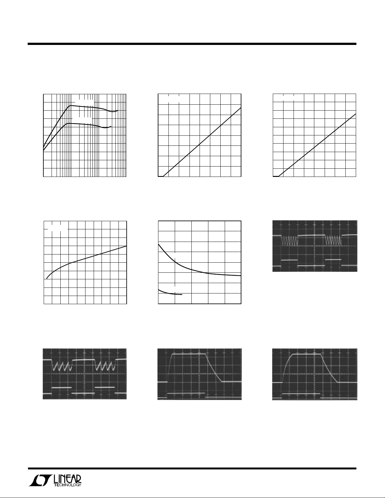
SHUTDOWN VOLTAGE (V)
0
SHUTDOWN CURRENT (µA)
0
4
6
8
20
12
14
2
4
5
LT1300 G3
2
16
18
10
13
6
7
8
T
A
= 25°C
U
TYPICAL PERFORMANCE CHARACTERISTICS
Total Quiescent Current
5V Output Efficiency
90
88
86
84
82
80
78
EFFICIENCY (%)
76
74
72
70
1
VIN = 3.3V
VIN = 2.5V
10 100 1000
LOAD CURRENT (mA)
LT1301 G1
Saturation Voltage vs Switch Current No-Load Input Current
250
TA = 25°C
225
200
175
150
125
100
75
SATURATION VOLTAGE (mV)
50
25
0
0 0.1
0.2 0.3
SWITCH CURRENT (A)
0.4 0.5
0.6 0.7
0.8 0.9
LT1301 G4
1
in Shutdown
80
TA = 25°C
70
60
(µA)
50
SENSE
+ I
40
VIN
+ I
30
SHDN
I
20
10
0
1
0
500
450
400
350
300
250
INPUT CURRENT (µA)
200
150
100
2
2
V
OUT
= 5V
V
OUT
34 6
4
3
INPUT VOLTAGE (V)
= 12V
5
INPUT VOLTAGE (V)
5
6
7
LT1301 G2
LT1301 G5
8
AC COUPLED
I
7
V
OUT
100mV/DIV
120mA
LOAD
0mA
LT1301
Shutdown Pin Bias Current
Load Transient Response of
Figure 1 Circuit
VIN = 5V
200µs/DIV
LT1301 G6
Load Transient Response of
Figure 1 Circuit
V
OUT
100mV/DIV
AC COUPLED
120mA
I
LOAD
0mA
VIN = 3.3V
Select Pin Transient Response
12V
V
OUT
2V/DIV
5V
V
SELECT
200µs/DIV
LT1301 G7
10V/DIV
C
= 100µF, VIN = 5V
OUT
100Ω LOAD
5ms/DIV
LT1301 G8
Select Pin Transient Response
12V
V
OUT
2V/DIV
5V
V
SELECT
10V/DIV
5ms/DIV
C
= 100µF, VIN = 3.3V
OUT
100Ω LOAD
LT1301 G9
3
LT1301
UUU
PIN FUNCTIONS
GND (Pin 1): Signal Ground. Tie to PGND under the
package.
Sel (Pin 2): Output Select. When tied to VIN converter
regulates at 12V. When grounded or floating converter
regulates at 5V. May be driven under logic control.
SHDN (Pin 3): Shutdown. Pull high to shut down the
LT1301. Ground for normal operation.
Sense (Pin 4): “Output” Pin. Goes to internal resistive
divider. If operating at 5V output, a 0.1µ F ceramic capacitor is required from Sense to Ground.
I
(Pin 5): Float for 1A switch current limit. Tie to ground
LIM
W
BLOCK DIAGRAM
V
IN
+
C1
for approximately 400mA. A resistor between I
LIM
and
ground sets peak current to some intermediate value .
VIN (Pin 6): Supply Pin. Must be bypassed with a large
value electrolytic to ground. Keep bypass within 0.2" of the
device.
SW (Pin 7): Switch Pin. Connect inductor and diode here.
Keep layout short and direct to minimize radio frequency
interference.
PGND (Pin 8): Power Ground. Tie to signal ground (pin 1)
under the package. Bypass capacitor from VIN should be
tied directly to PGND within 0.2" of the device.
L1
D1
V
OUT
+
C2
1.25V
REFERENCE
4
GND
1
SENSE
500k
97.5k
69.2k
SELECT
2
A1
COMPARATOR
+
–
ENABLE
V
IN
2
OFF
OSCILLATOR
155kHZ
SHUTDOWN
3
Figure 2.
A2 CURRENT
COMPARATOR
A3 DRIVER
BIAS
SW
7
18mV
+
R1
3Ω
R2
730Ω
–
Q1
Q2
160×
1×
Q3
8.5k
I
LIM
58
PGND
LT1301 F2
4
 Loading...