

Linear Technology LT1300 Datasheet
3.3/5V Step-Up DC/DC Converter
FEATURES
■
Up to 220mA Output Current at 5V from 2V Supply
■
Supply Voltage as Low as 1.8V
■
Up to 88% Efficiency
■
Small Inductor –10µH
■
120µA Quiescent Current
■
Shutdown to 10µA
■
Programmable 3.3V or 5V Output
■
I
Pin Programs Peak Switch Current
LIM
■
Low V
■
Uses Inexpensive Surface Mount Inductors
■
8-Lead DIP or SOIC Package
Switch: 170mV at 1A Typical
CESAT
U
APPLICATIONS
■
Palmtop Computers
■
Portable Instruments
■
Bar-Code Scanners
■
DC/DC Converter Module Replacements
■
Battery Backup Supplies
■
Personal Digital Assistants
■
PCMCIA Cards
LT1300
Micropower High Efficiency
U
DESCRIPTION
The LT1300 is a micropower step-up DC/DC converter that
utilizes Burst Mode™ operation. The device can deliver 5V
or 3.3V from a two-cell battery input. It features programmable 5V or 3.3V output via a logic-controlled input, noload quiescent current of 120µ A and a shutdown pin which
reduces supply current to 10µ A. The on-chip power switch
has a low 170mV saturation voltage at a switch current of
1A, a four-fold reduction over prior designs. A 155kHz
internal oscillator allows the use of extremely small surface mount inductors and capacitors. Operation is guaranteed at 1.8V input. This allows more energy to be extracted
from the battery increasing operating life. The I
be used to program peak switch current with a single
resistor allowing the use of less expensive and smaller
inductors and capacitors in lighter load applications. The
LT1300 is available in an 8-lead SOIC package, minimizing
board space requirements. For a 5V/12V Selectable Output Converter see the LT1301. For increased output current see the LT1302.
Burst Mode is a trademark of Linear Technology Corporation.
LIM
pin can
U
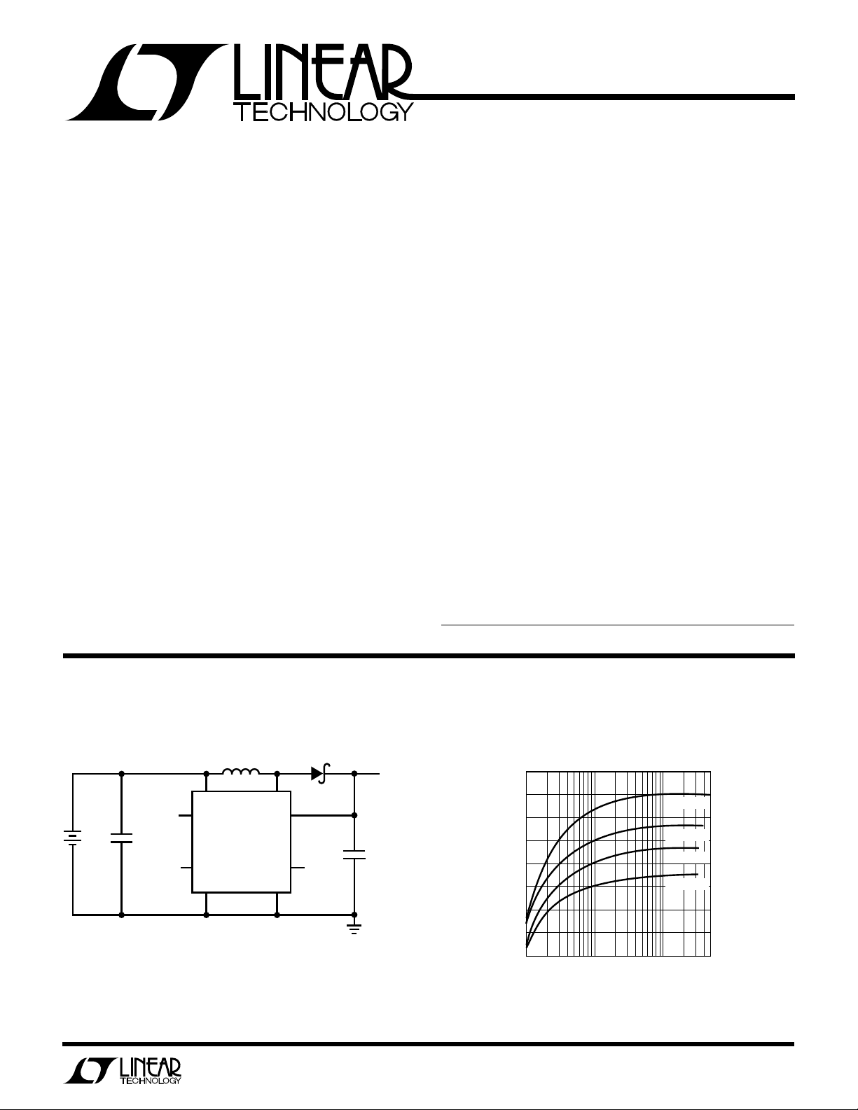
TYPICAL APPLICATIONS N
Two-Cell to 3.3V/5V Step-Up Converter 5V Output Efficiency
L1
10µH D1
5V/3.3V
2×
AA
CELL
L1 = COILCRAFT DO1608-103
OR SUMIDA CD54-100
C1 = AVX TPSD107M010R0100
OR SANYO OS-CON 16SA100M
D1 =MBRS130LT3
OR 1N5817
SELECT
+
C1
100µF
SHUTDOWN
67
V
IN
2
SELECT
LT1300
3
SHDN
PGND
81
SW
SENSE
I
LIM
GND
4
5
N/C
+
C1
100µF
5V/3.3V
OUTPUT
LT1300 TA1
90
88
86
84
82
80
EFFICIENCY (%)
78
76
74
1
VIN = 4.0V
VIN = 3.0V
VIN = 2.5V
VIN = 2.0V
10 100 500
LOAD CURRENT (mA)
LT1300 TA2
1
LT1300
WW
W
ABSOLUTE MAXIMUM RATINGS
VIN Voltage .............................................................. 10V
SW1 Voltage ............................................................ 20V
Sense Voltage .......................................................... 10V
SHUTDOWN Voltage................................................ 10V
SELECT Voltage ....................................................... 10V
I
Voltage ............................................................ 0.5V
LIM
Maximum Power Dissipation ............................. 500mW
Operating Temperature Range ..................... 0°C to 70°C
Storage Temperature Range ................. –65°C to 150°C
U
U
W
PACKAGE/ORDER INFORMATION
TOP VIEW
GND
1
SEL
2
SHDN
3
SENSE
4
N8 PACKAGE
8-LEAD PLASTIC DIP
T
= 100°C, θJA = 150°C/W
JMAX
PGND
8
SW
7
V
6
IN
I
5
LIM
S8 PACKAGE
8-LEAD PLASTIC SOIC
ORDER PART
NUMBER
LT1300CN8
LT1300CS8
S8 PART MARKING
1300
U
Lead Temperature (Soldering, 10 sec).................. 300°C
Consult factory for Industrial grade parts.
SEL
= 5V, V
TA = 25°C, V
SENSE
ELECTRICAL CHARACTERISTICS
SYMBOL PARAMETER CONDITIONS MIN TYP MAX UNITS
I
Q
VINInput Voltage Range 1.8 V
V
OUT
DC Maximum Duty Cycle 75 86 95 %
t
ON
V
CESAT
V
SHDNH
V
SHDNL
V
SELH
V
SELL
I
SHDN
I
SEL
The
temperature range.
Quiescent Current V
Output Sense Voltage V
Output Referred V
Comparator Hysteresis V
Oscillator Frequency Current Limit not Asserted. See Test Circuit. 120 155 185 kHz
Oscillator TC 0.2 %/°C
Switch On Time Current Limit not Asserted. 5.6 µs
Output Line Regulation 1.8V < VIN < 6V ● 0.06 0.15 %/V
Switch Saturation Voltage ISW = 700mA ● 130 200 mV
Switch Leakage Current VSW = 5V, Switch Off ● 0.1 10 µA
Peak Switch Current I
(Internal Trip Point) I
Shutdown Pin High ● 1.8 V
Shutdown Pin Low 0.5 V
Select Pin High ● 1.5 V
Select Pin Low ● 0.8 V
Shutdown Pin Bias Current V
Select Pin Bias Current 0V < V
● denotes specifications which apply over the 0°C to 70°C
= 0.5V, V
SHDN
V
= 1.8V ● 715 µA
SHDN
= 5V ● 4.80 5.0 5.20 V
SEL
V
= 0V ● 3.15 3.3 3.45 V
SEL
= 5V (Note 1) ● 22 50 mV
SEL
= 0V (Note 1) ● 14 35 mV
SEL
Floating (See Typical Application) 0.75 1.0 1.25 A
LIM
Grounded 0.4 A
LIM
= 5V ● 920 µA
SHDN
= 2V ● 3 µA
V
SHDN
V
= 0V ● 0.1 1 µA
SHDN
< 5V ● 13 µA
SEL
= 2V unless otherwise noted.
IN
= 5.5V ● 120 200 µA
● 2.0 V
Note 1: Hysteresis specified is DC. Output ripple may be higher if
output capacitance is insufficient or capacitor ESR is excessive. See
applications section.
2
W
INPUT VOLTAGE (V)
0
I
SHDN
+ I
VIN
+ I
SENSE
(µA)
40
50
60
8
LT1300 G3
30
20
0
2
4
6
10
80
70
1
3
5
7
INPUT VOLTAGE (V)
1.5
OUTPUT CURRENT (mA)
500
600
700
34
LT1300 G6
400
300
2
2.5
3.5 4.5
200
100
0
V
OUT
= 5V,
I
LIM
FLOATING
L = 22µH
COILCRAFT
DO3316-223
L = 10µH
COILCRAFT
DO1608-103
U
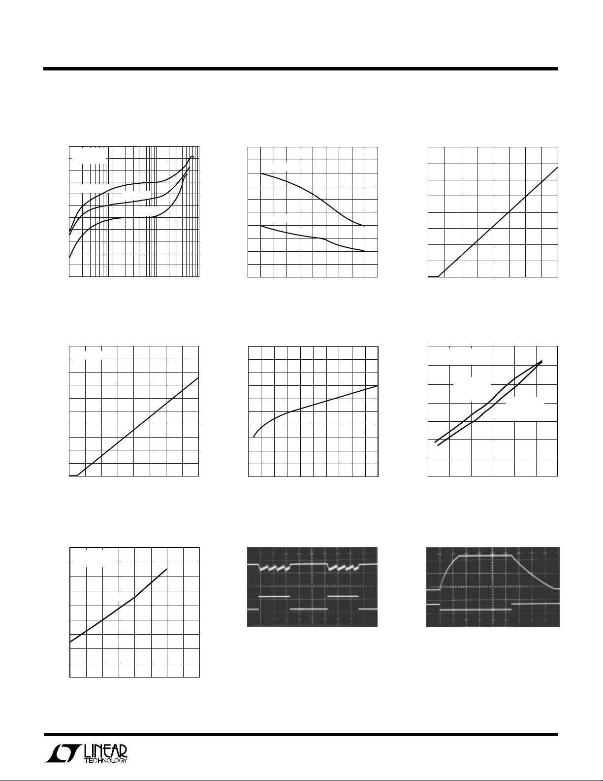
TYPICAL PERFORMANCE CHARACTERISTICS
Efficiency
88
V
= 3.3V
OUT
86
L = 10µH
84
82
VIN = 3V
80
78
76
74
EFFICIENCY (%)
72
70
68
66
1
VIN = 2.5V
10 100 1000
LOAD CURRENT (mA)
Shutdown Pin Bias Current
20
T
= 25°C
A
18
16
14
12
10
8
6
SHUTDOWN CURRENT (µA)
4
2
0
0
13
2
SHUTDOWN VOLTAGE (V)
VIN = 2V
4
5
LT1300 G1
7
6
LT1300 G4
8
No-Load Battery Current
170
165
160
155
150
145
140
135
INPUT CURRENT (µA)
130
125
120
250
225
200
175
150
(mV)
125
CESAT
100
V
75
50
25
1.4
V
0
CESAT
0 0.1
V
= 5V
OUT
V
= 3.3V
OUT
1.81.6
2.22.0
INPUT VOLTAGE (V)
vs I
SW
0.2 0.3
0.4 0.5
SWITCH CURRENT (A)
2.62.4
0.6 0.7
3.02.8
0.8 0.9
LT1300
Total Quiescent Current
in Shutdown
3.43.2
LT1300 G2
Maximum Output Current
vs Input Voltage
1
LT1300 G5
Maximum Output Current
vs Input Voltage
900
800
700
600
500
400
300
LOAD CURRENT (mA)
200
100
0
1.5
V
= 3.3V
OUT
I
FLOATING
LIM
L = 10µH
2
2.5
INPUT VOLTAGE (V)
Transient Response
VIN = 2V, V
V
OUT
100mV/DIV
AC COUPLED
200mA
I
LOAD
0
3.5
3
LT1300 G7
OUT
200µs/DIV
= 5V
LT1300 G8
Startup Response
V
OUT
1V/DIV
V
SHDN
10V/DIV
V
= 5V
OUT
= 20Ω
R
LOAD
500µs/DIV
LT1300 G9
3
 Loading...