

Linear Technology LT1268B, LT1268 Datasheet
LT1268B/LT1268
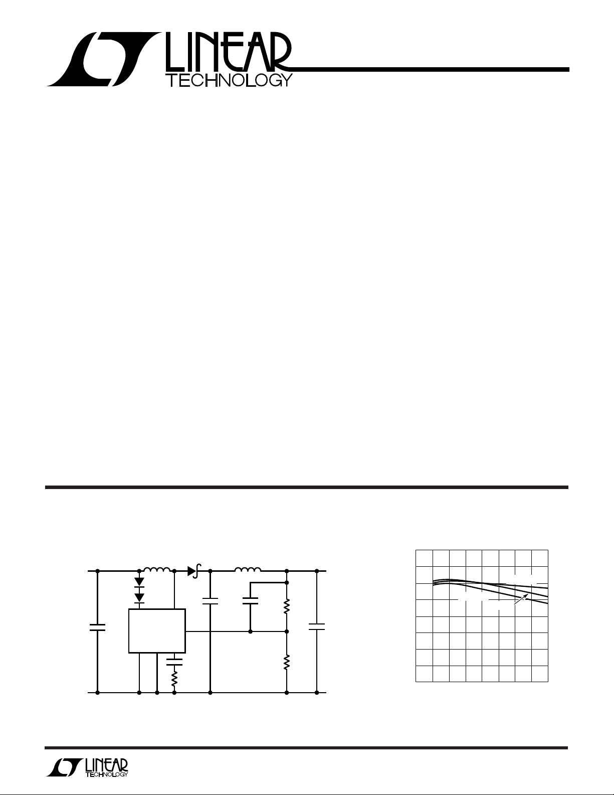
LOAD CURRENT (A)
0
EFFICIENCY (%)
80
90
4
LT1268 • TA02
70
60
1
2
3
100
VIN = 5.3V
VIN = 4.7V
VIN = 5V
7.5A, 150kHz
Switching Regulators
EATU
F
■
Wide Input Voltage Range: 3.5V to 30V
■
Low Quiescent Current: 7mA
■
Internal 7.5A Switch
■
Very Few External Parts Required
■
Self-Protected Against Overloads
■
Available in Standard and Surface Mount
RE
S
5-Pin Packages
■
Can Be Externally Synchronized
(See LT1072 Data Sheet)
U
O
PPLICATI
A
■
High Efficiency Boost Converter
■
PC Power Supply with Multiple Outputs
■
Battery Upconverter
■
Negative-to-Positive Converter
USER NOTE:
This data sheet is only intended to provide specifications, graphs, and a general functional
description of the LT1268B/LT1268. Application circuits are included to show the capability of the
LT1268B/LT1268. A complete design manual (AN19) should be obtained to assist in developing new
designs. This manual contains a comprehensive discussion of both the LT1070 and the external
components used with it, as well as complete formulas for calculating the values of these
components. The manual can also be used for the LT1268B/LT1268 factoring in the higher switch
current rating and higher operating frequency.
S
DUESCRIPTIO
The LT1268B and LT1268 are monolithic high power
switching regulators. Identical to the popular LT1070,
except for switching frequency (150kHz) and higher
switch current, they can be operated in all standard
switching configurations including buck, boost, flyback,
and inverting. A high current, high efficiency switch is
included on the die along with all oscillator, control, and
protection circuitry. Integration of all functions allows
the LT1268 to be built in standard 5-pin power packages.
This makes it extremely easy to use and provides “bust
proof” operations similar to that obtained with 3-pin
linear regulators.
The LT1268 operate with supply voltages from 3.5V to
30V and draw only 7mA quiescent current. By utilizing
current mode switching techniques, it provides excellent
AC and DC load and line regulation.
The LT1268 use an adaptive anti-sat switch drive to allow
very wide ranging load currents with no loss in efficiency.
An externally activated shutdown mode reduces total
supply current to 100µA typical for standby operation.
V
IN
4.7V TO
5.3V
U
O
A
PPLICATITYPICAL
Boost Regulator with 5.3V ±1% Output
†
V
MBR1035
SW
FB
C
R3
220Ω
D1
C2
0.068
C3
+
390µF
16V
C1
+
220µF
16V
L1
8µH, 5A*
D2, D3
1N4001
V
IN
LT1268B
CASE
GND V
COILTRONICS CTX8-5-52
*
COILTRONICS CTX2-5-52
**
†
OPTIONAL. D2 AND D3 ARE USED TO INCREASE
UNDERVOLTAGE LOCKOUT FROM 2.7V TO ≈4V.
L2
2µH, 5A**
C5
0.02
R1
4.043k
0.1%
R2
1.24k
0.1%
LT1268 • TA01
V
OUT
5.3V ±1%
3.75A
C4
+
390µF
16V
Efficiency of 5.3V Boost Converter
1
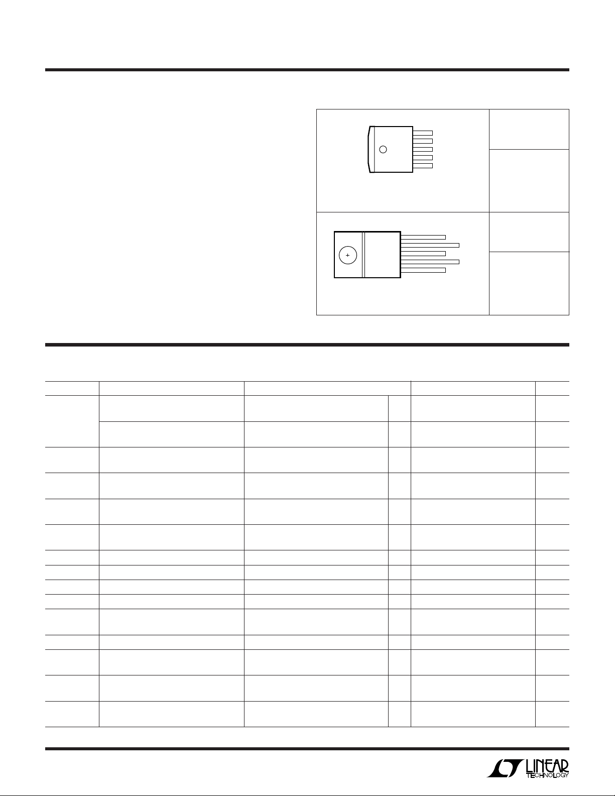
LT1268B/LT1268
Q PACKAGE
5-LEAD DD
FRONT VIEW
V
IN
V
SW
GND
FB
V
C
5
4
3
2
1
A
W
O
LUTEXI TIS
S
A
WUW
U
ARB
G
Supply Voltage ....................................................... 30V
Switch Output Voltage............................................ 60V
Feedback Pin Voltage (Transient, 1ms) ................ ±15V
Operating Junction Temperature Range
Operating............................................... 0°C to 125°C
Short-Circuit......................................... 0°C to 140°C
Storage Temperature Range................. –65°C to 150°C
Lead Temperature (Soldering, 10 sec)..................300°C
LECTRICAL C CHARA TERIST
E
ICS
VIN = 15V, VC = 0.5V, VFB = V
/
PACKAGE
T
= 125°C, θJC = 2°C/W, θJA = See Notes 5 and 6
JMAX
T
= 125°C, θJC = 2°C/W, θJA = 50°C/W
JMAX
Consult factory for Industrial and Military parts
O
RDER I FOR ATIO
FRONT VIEW
5
4
3
2
1
T PACKAGE
5-LEAD TO-220
, switch pin open, unless otherwise noted.
REF
V
IN
V
SW
GND
FB
V
C
WU
ORDER PART
NUMBER
LT1268CQ
LT1268BCQ
ORDER PART
NUMBER
LT1268CT
LT1268BCT
U
SYMBOL PARAMETER CONDITIONS MIN TYP MAX UNITS
V
REF
I
B
g
m
A
V
I
Q
BV Output Switch Breakdown Voltage 3V ≤ VIN ≤ V
V
SAT
I
LIM
2
Reference Voltage Measured at LT1268B 1.235 1.244 1.253 V
Feedback Pin (Note 4)
Reference Voltage LT1268 1.224 1.244 1.264 V
Feedback Input Current VFB = V
Error Amplifier Transconductance ∆IC = ±25µA 3000 4400 6000 µmho
Error Amplifier Source or Sink Current VC = 1.5V 150 200 350 µA
Error Amplifier Clamp Voltage Hi Clamp, VFB = 1V 1.80 2.30 V
Reference Voltage Line Regulation 3V ≤ VIN ≤ V
Error Amplifier Voltage Gain 0.9V ≤ VC ≤ 1.4V 500 800 V/V
Minimum Input Voltage ● 2.8 3.0 V
Supply Current 3V ≤ VIN ≤ V
Control Pin Threshold Duty Cycle = 0 0.7 0.9 1.08 V
Output Switch-ON Resistance TJ ≤ 100°C 0.12 0.18 Ω
(Note 1, 3) TJ ≤ 125°C 0.22 Ω
Control Voltage to Switch 12 A/V
Current Transconductance
Switch Current Limit (Note 3, 6) Duty Cycle = 50%, TJ ≤ 100°C ● 7.50 15 A
REF
Lo Clamp, VFB = 1.5V 0.25 0.38 0.52 V
, VC = 0.8V ● 0.03 %/V
MAX
, VC = 0.6V 7 10 mA
MAX
, ISW = 1.5mA ● 60 75 V
MAX
Duty Cycle = 65%, T
≤ 100°C ● 6.50 14 A
J
● 1.224 1.244 1.264 V
● 1.214 1.244 1.274 V
350 750 nA
● 1100 nA
● 2400 7000 µmho
● 120 400 µA
● 0.5 1.25 V
 Loading...