

Linear Technology LT1248 Datasheet
FEATURES
LT1248
Power Factor Controller
U
DESCRIPTIO
■
High Power Factor Over Wide Load Range
with Line Current Averaging
■
International Operation Without Switches
■
Instantaneous Overvoltage Protection
■
Minimal Line Current Dead Zone
■
Typical 250µA Start-Up Supply Current
■
Rejects Line Switching Noise
■
Synchronization Capability
■
Low Quiescent Current: 9mA
■
Fast 1.5A Peak Current Gate Driver
U
APPLICATIO S
■
Universal Power Factor Corrected Power Supplies
■
Preregulators Up To 1500W
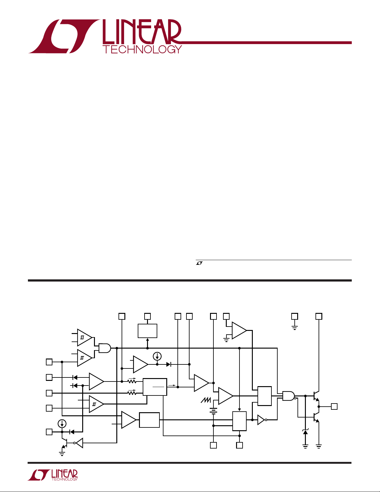
The LT®1248 provides active power factor correction for
universal off-line power systems. By using fixed high
frequency PWM current averaging, without the need for
slope compensation, the LT1248 achieves far lower line
current distortion with a smaller magnetic element than
systems that use either peak-current detection or zero
current switching approaches in both continuous and
discontinuous modes of operation.
The LT1248 uses a multiplier containing a square gain
function from the voltage amplifier to reduce the AC gain
at light output load and thus maintains low line current
distortion and high system stability. The LT1248 also
provides filtering capability to reject line switching noise
which can cause instability when fed into the multiplier.
Line current dead zone is minimized with low bias voltage
at the current input to the multiplier.
The LT1248 provides many protection features including
peak current limiting and overvoltage protection, and can
be operated at frequencies as high as 300kHz.
, LTC and LT are registered trademarks of Linear Technology Corporation.
BLOCK DIAGRA
+
V
CC
2.6V/
2.2V
7.5V
7.9V
12µA
–
–
+
–
EA
+
+
–
5V
16V TO 10V
EN/SYNC
10
V
SENSE
11
I
AC
6
OVP
8
SS
13
W
–
CA
+
CA
PK
OUT
32
–
+
+
0.7V
–
SYNC
C
SET
LIM
GND
1
–
+
R
R
Q
S
RUN
OSC
1 6V
1214
R
SET
V
CC
15
16
GTDR
1248 BD
M
OUTISENSE
4
5
7µA
I
2
M
I
A
B
2
32k
+
M1
–
I
A
I
B
ONE SHOT
V
REF
9
7.5V
V
REF
IM =
200ns
RUN
I
200µA
VA
OUT
7
2.2V
–
+
1
LT1248
A
W
O
LUTEXI TIS
S
A
WUW
ARB
U
G
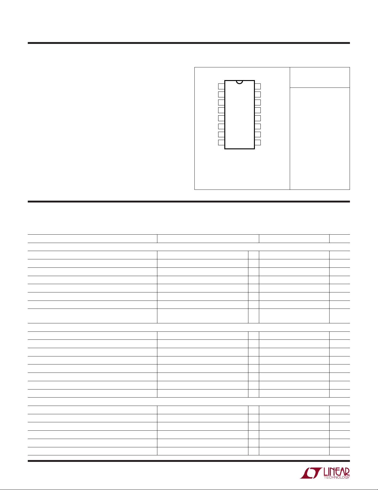
PACKAGE
/
O
RDER I FOR ATIO
WU
U
(Note 1)
Supply Voltage ....................................................... 27V
GTDR Current Continuous ..................................... 0.5A
GTDR Output Energy(Per Cycle) .............................. 5µJ
IAC, R
V
SENSE
I
SENSE
SET
, PK
Input Current............................. 20mA
LIM
, EN/SYNC, OVP Input Voltage................... V
, M
Input Current.................................. ±5mA
OUT
MAX
Operating Junction Temperature Range
LT1248C................................................ 0°C to 100°C
LT1248I ........................................... –40°C to 125°C
GND
PK
CA
I
SENSE
M
VA
OVP
LIM
OUT
OUT
I
OUT
AC
Thermal Resistance (Junction-to-Ambient)
N Package .................................................. 100°C/W
S Package................................................... 120°C/W
Storage Temperature Range ..................–65°C to 150°C
16-LEAD NARROW PLASTIC SO
T
T
Lead Temperature (Soldering, 10 sec)................. 300°C
Consult factory for Military grade parts.
LECTRICAL C CHARA TERIST
E
ture range, otherwise specifications are at T
C
= 1nF to GND, I
SET
PARAMETER CONDITIONS MIN TYP MAX UNITS
Overall
Supply Current (VCC in Undervoltage Lockout) VCC = Lockout Voltage – 0.2V ● 0.25 0.45 mA
Supply Current (Inactive) EN/SYNC = 0V, VCC ≤ V
Supply Current, On 11.5V ≤ VCC ≤ V
VCC Turn-On Threshold (Undervoltage Lockout) ● 15.5 16.5 17.5 V
VCC Turn-Off Threshold ● 9.5 10.5 11.5 V
EN/SYNC Threshold, Rising ● 2.2 2.6 2.85 V
EN/SYNC Threshold Hysteresis 0.40 V
EN/SYNC Input Current EN/SYNC = 0V ● –5 –1 5 µA
Voltage Amplifier
Voltage Amp Offset Voltage VA
Input Bias Current V
Voltage Gain 70 100 dB
Voltage Amp Unity-Gain Bandwidth 3 MHz
Voltage Amp Output High (Internally Clamped) ● 11.3 13.3 V
Voltage Amp Output Low ● 1.1 2 V
Voltage Amp Short-Circuit Current VA
SS Current SS = 2.5V ● 51230 µA
Current Amplifier
Current Amp Offset Voltage ● ±1 ±4mV
I
Bias Current ● – 25 –250 nA
SENSE
Current Amp Voltage Gain 80 110 dB
Current Amp Unity-Gain Bandwidth 3 MHz
Current Amp Output High ● 7.2 8.5 V
Current Amp Output Low ● 1.1 2 V
= 100µA, I
AC
SENSE
= 0V, CA
ICS
= 25°C. Maximum operating voltage (V
A
OUT
The ● denotes specifications which apply over the full operating tempera-
= 3.5V, VA
3V ≤ EN/SYNC ≤ 7V –50 – 25 50 µA
OUT
SENSE
OUT
= 5V, OVP = 7.5V, no load on any outputs, unless otherwise noted.
OUT
MAX
, CA
MAX
OUT
= 3.5V ● –8 8 mV
= 0V to 7V ● – 25 –250 nA
= 0V ● 51430 mA
TOP VIEW
1
2
3
4
5
6
7
8
N PACKAGE
16-LEAD PDIP
S PACKAGE
= 125°C, θJA = 100°C/W (N)
JMAX
= 125°C, θJA = 120°C/W (S)
JMAX
) = 25V, VCC = 18V, R
MAX
= 1V ● 8.5 12.0 mA
GTDR
16
V
15
CC
C
14
SET
SS
13
R
12
SET
V
11
SENSE
EN/SYNC
10
V
9
REF
● 0.5 1.5 mA
ORDER PART
NUMBER
LT1248CN
LT1248IN
LT1248CS
LT1248IS
= 15k to GND,
SET
2
LT1248
LECTRICAL C CHARA TERIST
E
ture range, otherwise specifications are at T
C
= 1nF to GND, I
SET
= 100µA, I
AC
SENSE
A
= 0V, CA
ICS
= 25°C. Maximum operating voltage (V
OUT
The ● denotes specifications which apply over the full operating tempera-
= 3.5V, VA
) = 25V, VCC = 18V, R
= 5V, OVP = 7.5V, no load on any outputs, unless otherwise noted.
OUT
MAX
= 15k to GND,
SET
PARAMETER CONDITIONS MIN TYP MAX UNITS
Current Amplifier
Current Amp Short-Circuit Current CA
Input Range, I
SENSE
, M
(Linear Operation) ● –0.3 1 V
OUT
= 0V ● 51430 mA
OUT
Reference
Reference Output Voltage I
V
Load Regulation –5mA < I
REF
V
Line Regulation 11.5V < VCC < V
REF
V
Short-Circuit Current V
REF
V
Worst Case Load, Line, Temperature ● 7.32 7.5 7.68 V
REF
= 0mA, TA = 25°C 7.39 7.50 7.60 V
REF
< 0mA 5 mV
REF
MAX
= 0V ● 12 28 50 mA
REF
● –20 5 20 mV
Current Limit
PK
Offset Voltage ● –15 15 mV
LIM
PK
Input Current PK
LIM
PK
to GTDR Propagation Delay PK
LIM
= –0.1V ● – 50 –100 µA
LIM
Falling from 50mV to –50mV 400 ns
LIM
Multiplier
Multiplier Output Current IAC = 100µA, R
= 15k 35 µA
SET
Multiplier Output Current Offset RAC = 1M from IAC to GND ● –0.05 –0.5 µA
Multiplier Maximum Output Current IAC = 450µA, R
= 15k, VA
SET
OUT
= 7V, M
= 0V ● –286 –260 – 235 µA
OUT
Multiplier Gain Constant (Note 2) 0.035 V
IAC Input Resistance IAC from 50µA to 1mA 15 32 50 kΩ
Oscillator
Oscillator Frequency R
C
Ramp Peak-to-Peak Amplitude 4.35 4.7 5.0 V
SET
C
Ramp Valley Voltage 1.25 1.4 1.55 V
SET
Synchronization Pulse Threshold on EN/SYNC Pin
Synchronization Frequency Range
SET
R
SET
= 15k, C
= 15k, C
= 1000pF ● 85 100 115 kHz
SET
= 1500pF ● 58 68 78 kHz
SET
Pulse Low = 3.5V, High = 7V, Width > 200ns
R
SET
= 15k, C
= 1000pF
SET
4.5 5.6 6.5 V
● 1.2 1.6 f
NOM
Overvoltage Comparator
Comparator Trip Voltage Ratio (V
TRIP/VREF
) ● 1.04 1.05 1.06
Hysteresis 0.35 V
OVP Bias Current OVP = 7.5V ● –50 – 250 nA
OVP Propagation Delay 100 ns
Gate Driver
Max GTDR Output Voltage 0mA Load, 18V < V
CC
GTDR Output High –200mA Load, 11.5V ≤ VCC ≤ 15V ● V
● 12 15 17.5 V
– 3.0 V
CC
GTDR Output Low (Device Unpowered) VCC = 0V, 50mA Load (Sinking) ● 0.9 1.5 V
GTDR Output Low (Device Active) 200mA Load (Sinking) ● 0.5 1 V
10mA Load
● 0.2 0.4 V
Peak GTDR Current 10nF from GTDR to GND 2 A
GTDR Rise and Fall Time 1nF from GTDR to GND 25 ns
GTDR Max Duty Cycle 90 96 %
–2
Note 1: Absolute Maximum Ratings are those values beyond which the life
of a device may be impaired
I
Note 2: Multiplier Gain Constant: K =
IAC (VA
M
OUT
– 2)
2
3

LT1248
LPER
UW
R
F
O
ATYPICA
CCHARA TERIST
E
C
ICS
Voltage Amplifier Open-Loop
Gain and Phase
100
80
60
40
GAIN (dB)
20
0
–20
10
100
GAIN
PHASE
1k 10k 100k
FREQUENCY (Hz)
Reference Voltage vs
Temperature
7.536
7.524
7.512
7.500
7.488
7.476
7.464
REFERENCE VOLTAGE (V)
7.452
7.440
7.428
–50 150
–75
0 25 50 100
–25
JUNCTION TEMPERATURE (°C)
75
1M 10M
1148 G01
125
1248 G03
0
–20
–40
–60
–80
–100
–120
PHASE (DEG)
Current Amplifier Open-Loop
Gain and Phase
100
80
GAIN
60
40
GAIN (dB)
–20
20
0
10
100
PHASE
1k 10k 100k
FREQUENCY (Hz)
Multiplier Current
300
VA
= 7V
OUT
VA
= 6.5V
OUT
VA
= 6V
OUT
150
(µA)
M
I
0
0
250
IAC (µA)
1M 10M
1148 G02
500
1248 G04
0
–20
–40
–60
–80
–100
–120
VA
VA
VA
VA
VA
VA
VA
OUT
OUT
OUT
OUT
OUT
OUT
OUT
PHASE (DEG)
= 5.5V
= 5V
= 4.5V
= 4V
= 3.5V
= 3V
= 2.5V
Supply Current vs Supply Voltage GTDR Source Current
11
10
TJ = –55°C
9
8
7
6
5
4
3
SUPPLY CURRENT (mA)
2
1
0
10
SUPPLY VOLTAGE (V)
TJ = 25°CTJ = 125°C
21
32
1248 G05
18.5
VCC = 18V
18.0
17.5
17.0
16.5
16.0
15.5
15.0
GTDR VOLTAGE (V)
14.5
14.0
13.5
13.0
0
–60
SOURCE CURRENT (mA)
4
TJ = 125°C
TJ = 25°C
TJ = –55°C
–120 –180 –240
1248 G06
–300
GTDR Sink Current
1.1
1.0
0.9
0.8
0.7
0.6
0.5
TA = –55°C
0.4
GTDR VOLTAGE (V)
0.3
0.2
0.1
0
TA = 125°C
0
TA = 25°C
60
120 180 240
SINK CURRENT (mA)
300
1248 G07
 Loading...