

Linear Technology LT1247, LT1246 Datasheet
LT1246/LT1247
1MHz Off-Line
Current Mode PWM
and DC/DC Converter
EATU
F
■
Current Mode Operation to 1MHz
■
30ns Current Sense Delay
■
< 250µA Low Start-Up Current
■
Current Sense Leading Edge Blanking
■
Pin Compatible with UC1842
■
Undervoltage Lockout with Hysteresis
■
No Cross-Conduction Current
■
Trimmed Bandgap Reference
■
1A Totem Pole Output
■
Trimmed Oscillator Frequency and Sink Current
■
Active Pull-Down on Reference and Output During
RE
S
Undervoltage Lockout
■
18V High Level Output Clamp
U
O
PPLICATI
A
■
Off-Line Converters
■
DC/DC Converters
Start-Up Operating Maximum
Device Threshold Voltage Duty Cycle Replaces
LT1246 16V 10V 100% UC1842
LT1247 8.4V 7.6V 100% UC1843
S
Minimum
DUESCRIPTIO
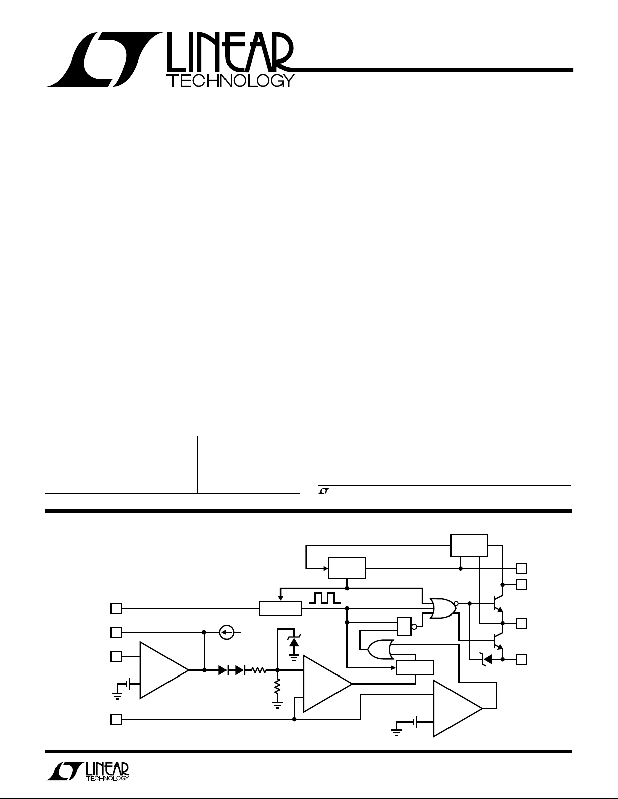
The LT®1246/LT1247 are 8-pin, fixed frequency, current
mode, pulse width modulators. These devices are designed to be improved plug compatible versions of the
industry standard UC1842 PWM circuit. The LT1246/
LT1247 are optimized for off-line and DC/DC converter
applications. They contain a temperature compensated
reference, high gain error amplifier, current sensing comparator, and a high current totem pole output stage ideally
suited to driving power MOSFETs. Start-up current has
been reduced to less than 250µ A. Cross-conduction current spikes in the totem pole output stage have been
eliminated, making 1MHz operation practical. Several new
features have been incorporated. Leading edge blanking
has been added to the current sense comparator. This
minimizes or eliminates the filter that is normally required.
Eliminating this filter allows the current sense loop to
operate with minimum delays. Trims have been added to
the oscillator circuit for both frequency and sink current,
and both of these parameters are tightly specified. The
output stage is clamped to a maximum V
on state. The output and the reference output are actively
pulled low during under-voltage lockout.
, LTC and LT are registered trademarks of Linear Technology Corporation.
of 18V in the
OUT
BLOCK
R
COMPENSATION
FEEDBACK
I
SENSE
IDAGRA
4
T/CT
1
2
3
2.5V
W
REFERENCE ENABLE
5V REF
MAIN BIAS
OSCILLATOR
5.6V
1mA
–
+
2R
R
1V
–
+
REFERENCE PULLDOWN
S
R
BLANKING
1.5V
LOCKOUT
OUTPUT
PULLDOWN
+
–
UV
18V
8
V
REF
7V
CC
6 OUTPUT
5 GND
LT1246 • BD01
1
LT1246/LT1247
WU
U
PACKAGE
/
O
RDER I FOR ATIO
A
W
O
LUTEXI T
S
A
WUW
ARB
U
G
I
S
Supply Voltage ....................................................... 25V
Output Current...................................................... ±1A*
Output Energy (Capacitive Load per Cycle)............. 5µJ
Analog Inputs (Pins 2, 3).............................. –0.3 to 6V
Error Amplifier Output Sink Current..................... 10mA
Power Dissipation at TA ≤ 25°C ............................... 1W
Operating Junction Temperature Range
LT1246C/LT1247C ............................. 0°C to 100°C
Storage Temperature Range ................ – 65°C to 150°C
Lead Temperature (Soldering, 10 sec)................. 300°C
*The 1A rating for output current is based on transient switching
requirements.
LECTRICAL C CHARA TERIST
E
ICS
(Notes 1, 2)
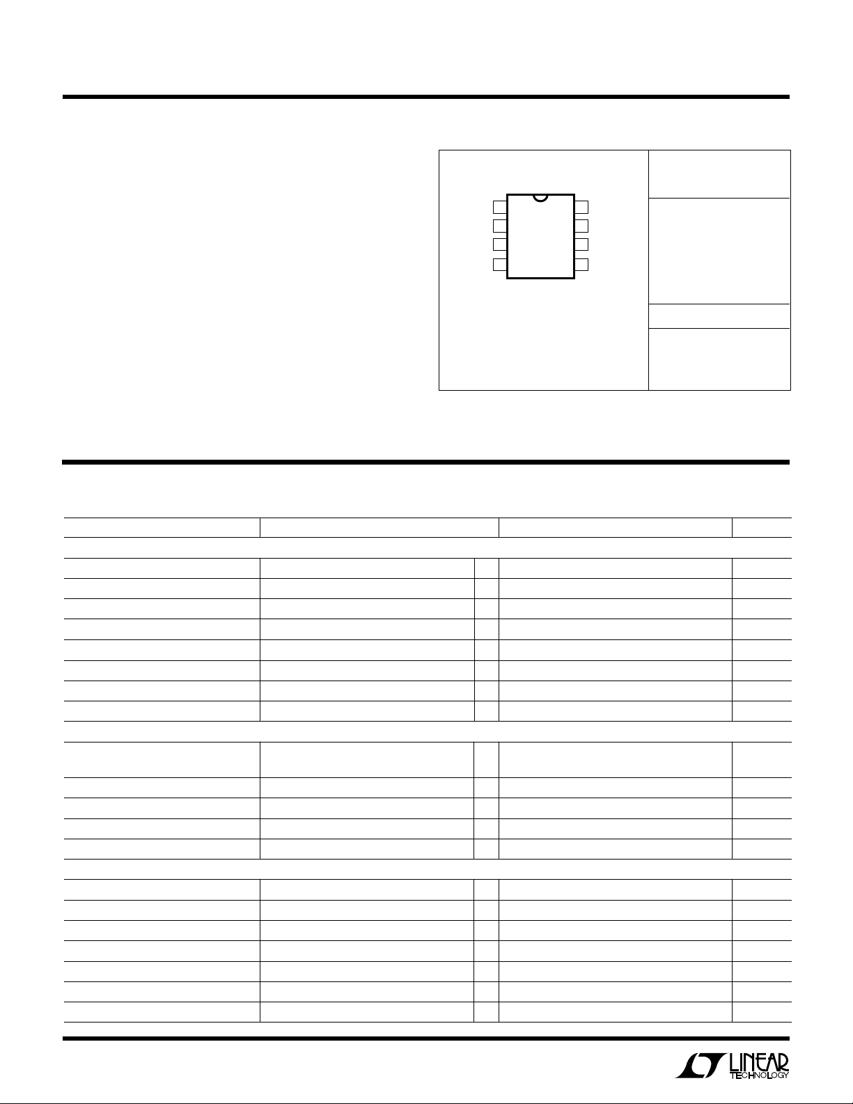
ORDER PART
TOP VIEW
V
COMP
1
FB
2
I
3
SENSE
R
4
T/CT
N8 PACKAGE
8-LEAD PDIP
S8 PACKAGE
8-LEAD PLASTIC SO
T
= 100°C, θJA = 130°C/W (N8)
JMAX
T
= 100°C, θJA = 150°C/W (S8)
JMAX
Consult factory for Industrial and Military grade parts.
8
7
6
5
REF
V
CC
OUTPUT
GND
NUMBER
LT1246CN8
LT1246CS8
LT1247CN8
LT1247CS8
S8 PART MARKING
1246
1247
PARAMETER CONDITIONS MIN TYP MAX UNITS
Reference Section
Output Voltage IO = 1mA, TJ = 25°C 4.925 5.000 5.075 V
Line Regulation 12V < VCC < 25V ● 320 mV
Load Regulation 1mA < I
Temperature Stability 0.1 mV/°C
Total Output Variation Line, Load, Temperature ● 4.87 5.13 V
Output Noise Voltage 10Hz < F < 10kHz, TJ = 25°C50µV
Long-Term Stability TA = 125°C, 1000 Hrs. 5 25 mV
Output Short-Circuit Current ● –30 –90 –180 mA
Oscillator Section
Initial Accuracy RT = 10k, CT = 3.3nF, TJ = 25°C 47.5 50 52.5 kHz
RT = 6.2k, CT = 500pF, TJ = 25°C 465 500 535 kHz
Voltage Stability 12V < VCC < 25V, TJ = 25°C1%
Temperature Stability T
Amplitude Pin 4 1.7 V
Clock Ramp Reset Current V
Error Amplifier Section
Feedback Pin Input Voltage V
Input Bias Current VFB = 2.5V ● –2 µA
Open-Loop Voltage Gain 2 < VO < 4V ● 65 90 dB
Unity-Gain Bandwidth TJ = 25°C 1 2 MHz
Power Supply Rejection Ratio 12V < VCC < 25V ● 60 dB
Output Sink Current V
Output Source Current V
MIN
OSC
PIN 1
PIN 2
PIN 2
< 20mA ● –6 –25 mV
REF
< TJ < T
MAX
(Pin 4) = 2V, TJ = 25°C 7.9 8.2 8.5 mA
= 2.5V ● 2.42 2.50 2.58 V
= 2.7V, V
= 2.3V, V
= 1.1V ● 26 mA
PIN 1
= 5V ● – 0.5 –0.75 mA
PIN 1
–0.05 %/°C
2
LT1246/LT1247
LECTRICAL C CHARA TERIST
E
PARAMETER CONDITIONS MIN TYP MAX UNITS
Error Amplifier Section
Output Voltage High Level V
Output Voltage Low Level V
Current Sense Section
Gain ● 2.85 3.00 3.15 V/V
Maximum Current Sense Input Threshold V
Power Supply Rejection Ratio 70 dB
Input Bias Current ● –1 –10 µA
Delay to Output 30 ns
Blanking Time 60 ns
Blanking Override Voltage 1.5 V
Output Section
Output Low Level I
Output High Level I
Rise Time CL = 1nF, TJ = 25°C3070ns
Fall Time CL = 1nF, TJ = 25°C2060ns
Output Clamp Voltage IO = 1mA ● 18 19 V
Undervoltage Lockout
Start-Up Threshold LT1246 ● 15 16 17 V
Minimum Operating Voltage LT1246 ● 9.0 10 11 V
Hysteresis LT1246 ● 5.5 6.0 V
PWM
Maximum Duty Cycle TJ = 25°C 94 100 %
Minimum Duty Cycle TJ = 25°C0%
Total Device
Start-Up Current ● 170 250 µA
Operating Current ● 13 20 mA
PIN 2
PIN 2
PIN 3
= 20mA ● 0.25 0.4 V
OUT
= 200mA ● 0.75 2.2 V
I
OUT
= 20mA ● 12.0 V
OUT
= 200mA ● 11.75 V
I
OUT
LT1247
LT1247
LT1247
ICS
(Notes 1, 2)
= 2.3V, RL = 15k to GND ● 5 5.6 V
= 2.7V, RL = 15k to Pin 8 ● 0.2 1.1 V
< 1.1V ● 0.90 1.00 1.10 V
● 7.8 8.4 9.0 V
● 7.0 7.6 8.2 V
● 0.4 0.8 V
The ● denotes those specifications which apply over the full operating
temperature range.
Note 1: Unless otherwise specified, V
= 15V, RT = 10k, CT = 3.3nF.
CC
Note 2: Low duty cycle pulse techniques are used during test to maintain
junction temperature close to ambient.
3
LT1246/LT1247
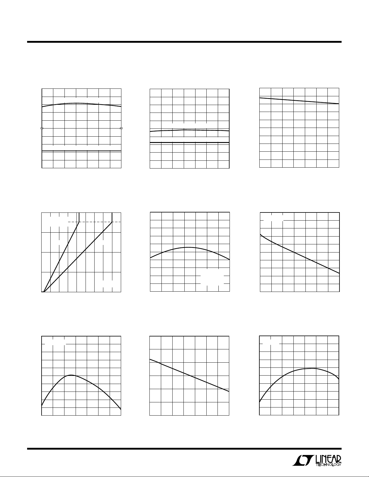
TEMPERATURE (°C)
–50
–10
FREQUENCY CHANGE (%)
–6
–2
2
6
10
–25 25 75 125
LT1246 • TPC06
0 50 100
–8
–4
0
4
8
VCC = 15V
UW
Y
PICA
17
16
15
(V)
CC
V
11
10
9
200
150
100
LPER
F
O
R
AT
CCHARA TERIST
E
C
ICS
LT1246 Undervoltage Lockout LT1247 Undervoltage Lockout Start-Up Current
200
180
160
140
120
100
80
60
START-UP CURRENT (µA)
40
20
0
–25 25 75 125
–50
START-UP THRESHOLD
MINIMUM OPERATING VOLTAGE
–50
0 50 100
–25 25 75 125
TEMPERATURE (°C)
LT1246 • TPC01
(V)
CC
V
11
10
9
8
7
6
–50
START-UP THRESHOLD
MINIMUM OPERATING VOLTAGE
–25 25 75 125
0 50 100
TEMPERATURE (°C)
1247 TPC02
Start-Up Current Supply Current Oscillator Frequency
15
START-UP
THRESHOLD
LT1246LT1247
14
13
(mA)
CC
I
12
0 50 100
TEMPERATURE (°C)
LT1246 • TPC03
50
START-UP CURRENT (µA)
0
0
Oscillator Sink Current Reference Short-Circuit Current Reference Voltage
8.7
8.6
8.5
8.4
8.3
8.2
8.1
8.0
7.9
OSCILLATOR SINK CURRENT (mA)
7.8
7.7
–50
4
TJ = 25°C
410146 16
2 8 12 18
VCC (V)
V
= 2V
PIN 4
0 50 100
–25 25 75 125
TEMPERATURE (°C)
1246/7 TPC04
LT1246 • TPC07
11
10
–25 25 75 125
–50
140
120
100
80
60
40
REFERENCE SHORT-CIRCUIT CURRENT (mA)
20
–50
0 50 100
TEMPERATURE (°C)
0 50 100
–25 25 75 125
TEMPERATURE (°C)
VCC = 15V
= 10k
R
T
= 3300pF
C
T
LT1246 • TPC05
LT1246 • TPC08
5.05
5.04
5.03
5.02
5.01
5.00
4.99
4.98
REFERENCE VOLTAGE (V)
4.97
4.96
4.95
–50
IO = 1mA
0 50 100
–25 25 75 125
TEMPERATURE (°C)
LT1246 • TPC09
 Loading...