

Linear Technology LT1228 Datasheet
LT1228
100MHz Current Feedback
Amplifier with DC Gain Control
EATU
F
■
Very Fast Transconductance Amplifier
RE
S
Bandwidth: 75MHz
gm = 10 × I
Low THD: 0.2% at 30mV
Wide I
■
Very Fast Current Feedback Amplifier
SET
Range: 1µA to 1mA
SET
RMS
Input
Bandwidth: 100MHz
Slew Rate: 1000V/µs
Output Drive Current: 30mA
Differential Gain: 0.04%
Differential Phase: 0.1°
High Input Impedance: 25MΩ, 6pF
■
Wide Supply Range: ±2V to ±15V
■
Inputs Common Mode to Within 1.5V of Supplies
■
Outputs Swing Within 0.8V of Supplies
■
Supply Current: 7mA
U
O
PPLICATI
A
■
Video DC Restore (Clamp) Circuits
■
Video Differential Input Amplifiers
■
Video Keyer/Fader Amplifiers
■
AGC Amplifiers
■
Tunable Filters
■
Oscillators
S
DUESCRIPTIO
The LT1228 makes it easy to electronically control the gain
of signals from DC to video frequencies. The LT1228
implements gain control with a transconductance amplifier
(voltage to current) whose gain is proportional to an externally controlled current. A resistor is typically used to
convert the output current to a voltage, which is then
amplified with a current feedback amplifier. The LT1228
combines both amplifiers into an 8-pin package, and operates on any supply voltage from 4V (±2V) to 30V (±15V). A
complete differential input, gain controlled amplifier can be
implemented with the LT1228 and just a few resistors.
The LT1228 transconductance amplifier has a high impedance differential input and a current source output with wide
output voltage compliance. The transconductance, gm, is
set by the current that flows into pin 5, I
gm is equal to ten times the value of I
holds over several decades of set current. The voltage at pin
5 is two diode drops above the negative supply, pin 4.
The LT1228 current feedback amplifier has very high input
impedance and therefore it is an excellent buffer for the
output of the transconductance amplifier. The current feedback amplifier maintains its wide bandwidth over a wide
range of voltage gains making it easy to interface the
transconductance amplifier output to other circuitry. The
current feedback amplifier is designed to drive low impedance loads, such as cables, with excellent linearity at high
frequencies.
. The small signal
SET
and this relationship
SET
U
O
A
PPLICATITYPICAL
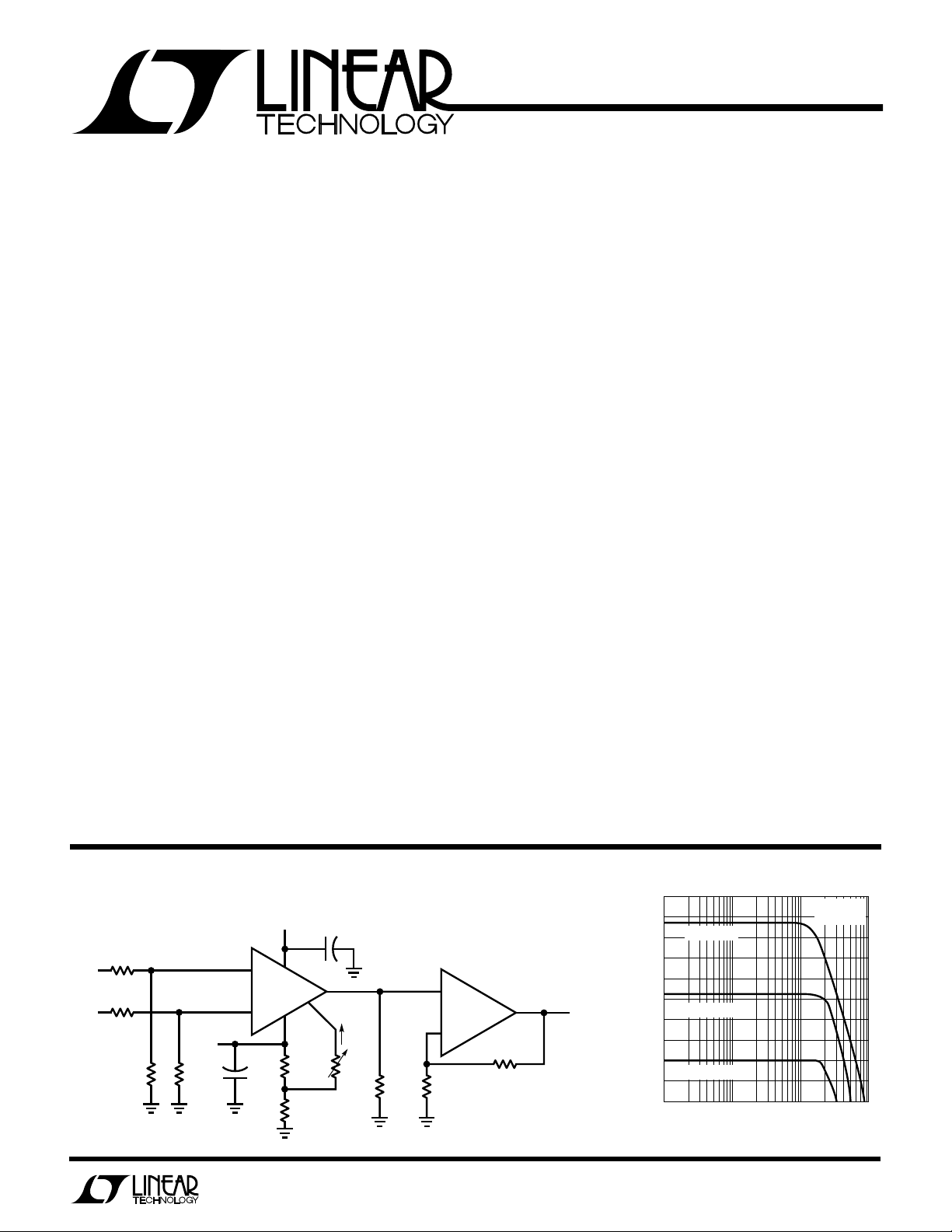
Differential Input Variable Gain Amp
15V
4.7µF
m
7
4
R4
1.24k
R6
6.19Ω
+
1
+
5
I
SET
R5
10k
R1
270Ω
CFA V
8
–
RG
10Ω
6
R
F
470Ω
HIGH INPUT RESISTANCE
EVEN WHEN POWER IS OFF
–18dB < GAIN < 2dB
≤ 3V
V
IN
RMS
OUT
LT1228 • TA01
R3A
10k
+
R2A
V
IN
10k
–
–15V
100Ω
R3
R2
100Ω
3
+
g
2
–
4.7µF
+
6
3
0
–3
–6
–9
GAIN (dB)
–12
–15
–18
–21
–24
100k
Frequency Response
= 1mA
I
SET
I
= 300µA
SET
I
= 100µA
SET
1M 10M 100M
FREQUENCY (Hz)
= ±15V
V
S
= 100Ω
R
L
LT1228 • TA02
1
LT1228
WU
U
PACKAGE
/
O
RDER I FOR ATIO
W
O
A
LUTEXI T
S
Supply Voltage ...................................................... ±18V
Input Current, Pins 1, 2, 3, 5, 8 (Note 7) ............ ±15mA
Output Short Circuit Duration (Note 1) .........Continuous
Operating Temperature Range
LT1228C................................................ 0°C to 70°C
LT1228M........................................ –55°C to 125°C
Storage Temperature Range ................. –65°C to 150°C
Junction Temperature
Plastic Package .............................................. 150°C
Ceramic Package ............................................175°C
Lead Temperature (Soldering, 10 sec)..................300°C
LECTRICAL C CHARA TERIST
E
Current Feedback Amplifier, Pins 1, 6, 8. ±5V ≤ VS ≤ ±15V, I
SYMBOL PARAMETER CONDITIONS MIN TYP MAX UNITS
V
OS
+
I
IN
–
I
IN
e
n
i
n
R
IN
C
IN
CMRR Common-Mode Rejection Ratio VS = ±15V, V
PSRR Power Supply Rejection Ratio VS = ±2V to ±15V, TA = 25°C6080dB
Input Offset Voltage TA = 25°C ±3 ±10 mV
Input Offset Voltage Drift ● 10 µV/°C
Noninverting Input Current TA = 25°C ±0.3 ±3 µA
Inverting Input Current TA = 25°C ±10 ±65 µA
Input Noise Voltage Density f = 1kHz, RF = 1k, RG = 10Ω, RS = 0Ω 6 nV/√Hz
Input Noise Current Density f = 1kHz, RF = 1k, RG = 10Ω, RS = 10k 1.4 pV/√Hz
Input Resistance V
Input Capacitance (Note 2) VS = ±5V 6 pF
Input Voltage Range VS = ±15V, TA = 25°C ±13 ±13.5 V
Inverting Input Current VS = ±15V, V
Common-Mode Rejection V
Noninverting Input Current VS = ±2V to ±15V, TA = 25°C 10 50 nA/V
Power Supply Rejection V
Inverting Input Current VS = ±2V to ±15V, TA = 25°C 0.1 5 µA/V
Power Supply Rejection VS = ±3V to ±15V ● 5 µA/V
A
WUW
U
ARB
G
I
S
TOP VIEW
1I
OUT
2
–IN
+IN
–
V
J8 PACKAGE
8-LEAD CERAMIC DIP
T
T
J MAX =
T
J MAX =
Consult Factory for Industrial grade parts.
g
m
3
S8 PACKAGE
8-LEAD PLASTIC SOIC
175°C, θ
J MAX =
150°C, θ
150°C, θ
8
7
6
54
N8 PACKAGE
100°C/W (J)
100°C/W (N)
150°C/W (S)
GAIN
+
V
V
OUT
I
SET
+–
8-LEAD PLASTIC DIP
JA =
JA =
JA =
ORDER PART
NUMBER
LT1228MJ8
LT1228CJ8
LT1228CN8
LT1228CS8
S8 PART MARKING
1228
ICS
= 0µA, VCM = 0V unless otherwise noted.
SET
● ±15 mV
● ±10 µA
● ±100 µA
= ±13V, VS = ±15V ● 225 MΩ
IN
= ±3V, VS = ±5V ● 225 MΩ
V
IN
● ±12 V
VS = ±5V, TA = 25°C ±3 ±3.5 V
● ±2V
= ±13V, TA = 25°C5569dB
= ±15V, V
V
S
= ±5V, V
V
S
= ±5V, V
V
S
= ±15V, V
S
= ±5V, V
V
S
VS = ±5V, V
= ±3V to ±15V ● 60 dB
V
S
= ±3V to ±15V ● 50 nA/V
S
CM
= ±12V ● 55 dB
CM
= ±3V, TA = 25°C5569dB
CM
= ±2V ● 55 dB
CM
= ±13V, TA = 25°C 2.5 10 µA/V
CM
= ±12V ● 10 µA/V
CM
= ±3V, TA = 25°C 2.5 10 µA/V
CM
= ±2V ● 10 µA/V
CM
2
LT1228
LECTRICAL C CHARA TERIST
E
Current Feedback Amplifier, Pins 1, 6, 8. ±5V ≤ VS ≤ ±15V, I
SYMBOL PARAMETER CONDITIONS MIN TYP MAX UNITS
A
V
R
OL
V
OUT
I
OUT
I
s
SR Slew Rate (Notes 3 and 5) TA = 25°C 300 500 V/µs
SR Slew Rate VS = ±15V, RF = 750Ω, RG= 750Ω, RL = 400Ω 3500 V/µs
t
r
BW Small-Signal Bandwidth VS = ±15V, RF = 750Ω, RG= 750Ω, RL = 100Ω 100 MHz
t
r
t
s
Large-Signal Voltage Gain VS = ±15V, V
Transresistance, ∆V
Maximum Output Voltage Swing VS = ±15V, R
Maximum Output Current R
Supply Current V
Rise Time (Notes 4 and 5) TA = 25°C1020ns
Small-Signal Rise Time VS = ±15V, RF = 750Ω, RG= 750Ω, RL = 100Ω 3.5 ns
Propagation Delay VS = ±15V, RF = 750Ω, RG= 750Ω, RL = 100Ω 3.5 ns
Small-Signal Overshoot VS = ±15V, RF = 750Ω, RG= 750Ω, RL = 100Ω 15 %
Settling Time 0.1%, V
Differential Gain (Note 6) VS = ±15V, RF = 750Ω, RG= 750Ω, RL = 1k 0.01 %
Differential Phase (Note 6) VS = ±15V, RF = 750Ω, RG= 750Ω, RL = 1k 0.01 DEG
Differential Gain (Note 6) VS = ±15V, RF = 750Ω, RG= 750Ω, RL = 150Ω 0.04 %
Differential Phase (Note 6) VS = ±15V, RF = 750Ω, RG= 750Ω, RL = 150Ω 0.1 DEG
OUT
/∆I
–
IN
ICS
= 0µA, VCM = 0V unless otherwise noted.
SET
= ±10V, R
VS = ±5V, V
VS = ±15V, V
= ±5V, V
V
S
= ±5V, R
V
S
LOAD
OUT
OUT
= ±2V, R
OUT
= ±10V, R
OUT
= ±2V, R
OUT
= 400Ω, TA = 25°C ±12 ±13.5 V
LOAD
= 150Ω, TA = 25°C ±3 ±3.7 V
LOAD
= 0Ω, TA = 25°C 30 65 125 mA
= 0V, I
= 0V ● 611 mA
SET
= 10V, RF =1k, RG= 1k, RL =1k 45 ns
OUT
= 1k ● 55 65 dB
LOAD
= 150Ω ● 55 65 dB
LOAD
= 1k ● 100 200 kΩ
LOAD
= 150Ω ● 100 200 kΩ
LOAD
● ±10 V
● ±2.5 V
● 25 125 mA
LECTRICAL C CHARA TERIST
E
Transconductance Amplifier, Pins 1, 2, 3, 5. ±5V ≤ VS ≤ ±15V, I
SYMBOL PARAMETER CONDITIONS MIN TYP MAX UNITS
V
OS
I
OS
I
B
e
n
R
IN
C
IN
Input Offset Voltage I
Input Offset Voltage Drift ● 10 µV/°C
Input Offset Current TA = 25°C 40 200 nA
Input Bias Current TA = 25°C 0.4 1 µA
Input Noise Voltage Density f = 1kHz 20 nV/√Hz
Input Resistance-Differential Mode V
Input Resistance-Common Mode VS = ±15V, VCM = ±12V ● 50 1000 MΩ
Input Capacitance 3pF
Input Voltage Range VS = ±15V, TA = 25°C ±13 ±14 V
ICS
= 100µA, VCM = 0V unless otherwise noted.
SET
= 1mA, TA = 25°C ±0.5 ±5mV
SET
≈ ±30mV ● 30 200 kΩ
IN
= ±5V, VCM = ±2V ● 50 1000 MΩ
V
S
= ±15V ● ±12 V
V
S
= ±5V, TA = 25°C ±3 ±4V
V
S
= ±5V ● ±2V
V
S
● ±10 mV
● 500 nA
● 5 µA
3
LT1228
LECTRICAL C CHARA TERIST
E
Transconductance Amplifier, Pins 1, 2, 3, 5. ±5V ≤ VS ≤ ±15V, I
SYMBOL PARAMETER CONDITIONS MIN TYP MAX UNITS
CMRR Common-Mode Rejection Ratio VS = ±15V, V
PSRR Power Supply Rejection Ratio VS = ±2V to ±15V, TA = 25°C 60 100 dB
g
m
I
OUT
I
OL
V
OUT
R
O
I
S
THD Total Harmonic Distortion VIN = 30mV
BW Small-Signal Bandwidth R1 = 50Ω, I
t
r
Transconductance I
Transconductance Drift ● –0.33 %/°C
Maximum Output Current I
Output Leakage Current I
Maximum Output Voltage Swing VS = ±15V , R1 = ∞ ● ±13 ±14 V
Output Resistance VS = ±15V, V
Output Capacitance (Note 2) VS = ±5V 6 pF
Supply Current, Both Amps I
Small-Signal Rise Time R1 = 50Ω, I
Propagation Delay R1 = 50Ω, I
ICS
= 100µA, VCM = 0V unless otherwise noted.
SET
= ±13V, TA = 25°C 60 100 dB
= ±15V, V
V
S
= ±5V, V
V
S
VS = ±5V, V
= ±3V to ±15V ● 60 dB
V
S
= 100µA, I
SET
= 100µA ● 70 100 130 µA
SET
= 0µA (+IIN of CFA), TA = 25°C 0.3 3 µA
SET
= ±5V , R1 = ∞ ● ±3 ±4V
V
S
= ±5V, V
V
S
= 1mA ● 915 mA
SET
CM
= ±12V ● 60 dB
CM
= ±3V, TA = 25°C 60 100 dB
CM
= ±2V ● 60 dB
CM
= ±30µA, TA = 25°C 0.75 1.00 1.25 µA/mV
OUT
● 10 µA
= ±13V ● 28 MΩ
OUT
= ±3V ● 28 MΩ
OUT
at 1kHz, R1 = 100k 0.2 %
RMS
= 500µA 80 MHz
SET
= 500µA, 10% to 90% 5 ns
SET
= 500µA, 50% to 50% 5 ns
SET
The ● denotes specifications which apply over the operating temperature
range.
Note 1: A heat sink may be required depending on the power supply
voltage.
Note 2: This is the total capacitance at pin 1. It includes the input
capacitance of the current feedback amplifier and the output capacitance
of the transconductance amplifier.
Note 3: Slew rate is measured at ±5V on a ±10V output signal while
operating on ±15V supplies with R
slew rate is much higher when the input is overdriven, see the applications
section.
= 1k, RG = 110Ω and RL = 400Ω. The
F
Note 4: Rise time is measured from 10% to 90% on a ±500mV output
signal while operating on ±15V supplies with R
RL = 100Ω. This condition is not the fastest possible, however, it does
guarantee the internal capacitances are correct and it makes automatic
testing practical.
Note 5: AC parameters are 100% tested on the ceramic and plastic DIP
packaged parts (J and N suffix) and are sample tested on every lot of
the SO packaged parts (S suffix).
Note 6: NTSC composite video with an output level of 2V.
Note 7: Back to back 6V Zener diodes are connected between pins 2 and
3 for ESD protection.
= 1k, RG = 110Ω and
F
4
LT1228
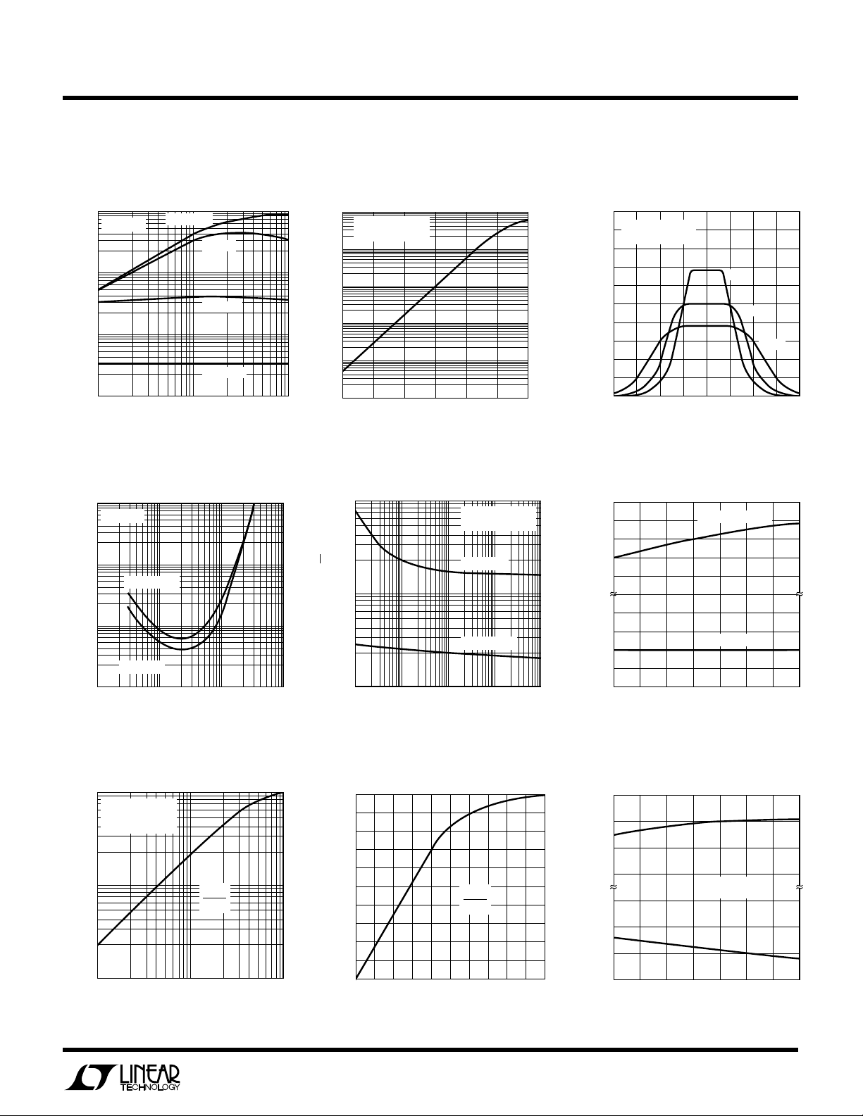
TEMPERATURE (°C)
–50
V
–
COMMON-MODE RANGE (V)
0.5
1.0
–1.5
V
+
–25 0 25 125
LT1228 • TPC06
50 75 100
–0.5
–1.0
–2.0
1.5
2.0
V
–
= –2V TO –15V
V+ = 2V TO 15V
INPUT VOLTAGE (mVDC)
–200
0
TRANSCONDUCTANCE (µA/mV)
0.2
0.4
1.4
2.0
–150 –100 –50 200
LT1228 • TPC03
0 100 150
1.8
1.6
1.2
0.6
0.8
–55°C
VS = ±2V TO ±15V
I
SET
= 100µA
50
1.0
25°C
125°C
TEMPERATURE (°C)
–50
V
–
OUTPUT SATURATION VOLTAGE (V)
+0.5
+1.0
–1.0
V
+
–25 0 25 125
LT1228 • TPC09
50 75 100
–0.5
±2V ≤ VS ≤ ±15V
R1 =
∞
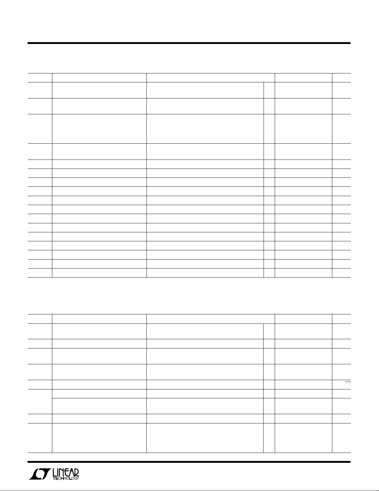
UW
Y
PICA
100
10
1
–3dB BANDWIDTH (MHz)
LPER
F
O
R
AT
CCHARA TERIST
E
C
ICS
Transconductance Amplifier, Pins 1, 2, 3 & 5
Small-Signal Bandwidth vs Small-Signal Transconductance Small-Signal Transconductance
Set Current and Set Current vs Bias Voltage vs DC Input Voltage
VS = ±15V
R1 = 100Ω
R1 = 1k
R1 = 10k
R1 = 100k
100
10
0.1
0.01
TRANSCONDUCTANCE (µA/mV)
1
VS = ±2V TO ±15V
= 25°C
T
A
10000
1000
SET CURRENT (µA)
100
10
1.0
0.1
10
Total Harmonic Distortion vs Spot Output Noise Current vs Input Common-Mode Limit vs
Input Voltage Frequency Temperature
10
VS = ±15V
1
I
= 100µA
SET
0.1
OUTPUT DISTORTION (%)
I
= 1mA
SET
0.01
1
INPUT VOLTAGE (mV
Small-Signal Control Path Small-Signal Control Path Output Saturation Voltage vs
Bandwidth vs Set Current Gain vs Input Voltage Temperature
100
VS = ±2V TO ±15V
= 200mV
V
IN
(PIN 2 TO 3)
10
–3dB BANDWIDTH (MHz)
1
10
100 1000
SET CURRENT (µA)
10 1000
∆I
∆I
100 1000
SET CURRENT (µA)
100
OUT
SET
P–P
LT1228 • TPC01
)
LT1228 • TPC04
LT1228 • TPC07
0.001
1.0 1.1 1.4
0.9 1.2 1.3 1.5
BIAS VOLTAGE, PIN 5 TO 4, (V)
1000
100
SPOT NOISE (pA/√Hz)
1.0
0.9
0.8
0.7
0.6
0.5
0.4
0.3
0.2
CONTROL PATH GAIN (µA/µA)
0.1
10
10
0
100 10k
FREQUENCY (Hz)
40 80 160
0
INPUT VOLTAGE, PIN 2 TO 3, (mVDC)
VS = ±2V TO ±15V
= 25°C
T
A
I
SET
I
SET
1k 100k
∆I
OUT
∆I
SET
120 200
0.1
LT1228 • TPC02
= 1mA
= 100µA
LT1228 • TPC05
LT1228 • TPC08
5
LT1228
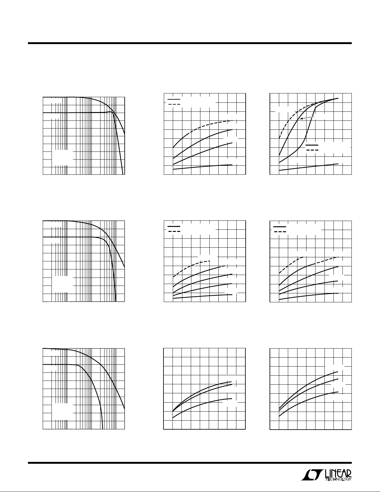
SUPPLY VOLTAGE (±V)
2
–3dB BANDWIDTH (MHz)
40
100
120
12 16
LT1228 • TPC12
4068101418
0
20
60
140
160
180
80
PEAKING ≤ 0.5dB
PEAKING ≤ 5dB
RF = 750Ω
RF = 1k
RF = 2k
RF = 500Ω
SUPPLY VOLTAGE (±V)
2
–3dB BANDWIDTH (MHz)
40
100
120
12 16
LT1228 • TPC15
4068101418
0
20
60
140
160
180
RF = 500Ω
80
PEAKING ≤ 0.5dB
PEAKING ≤ 5dB
RF = 750Ω
RF = 1k
RF = 2k
RF = 250Ω
SUPPLY VOLTAGE (±V)
2
–3dB BANDWIDTH (MHz)
4
10
12
12 16
LT1228 • TPC18
4068101418
0
2
6
14
16
18
RF = 500Ω
8
RF = 1k
RF = 2k
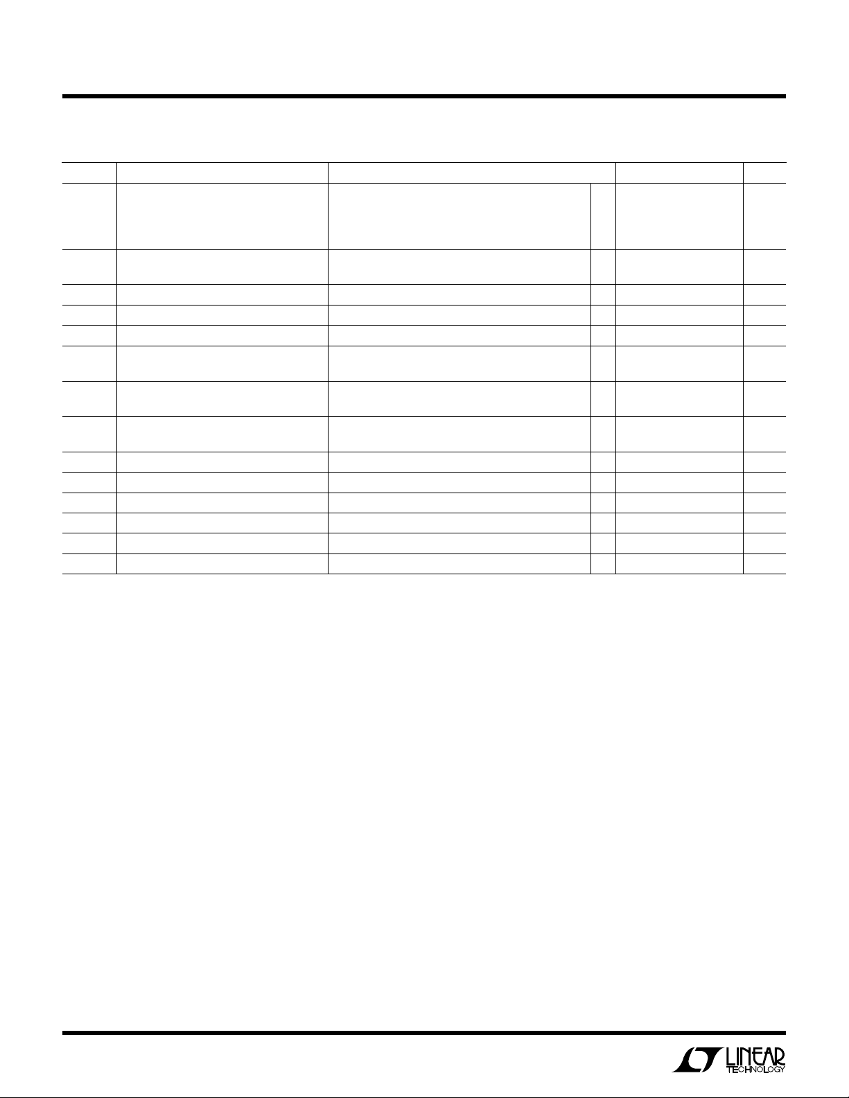
UW
Y
PICA
8
7
6
5
4
3
2
VOLTAGE GAIN (dB)
1
0
–1
–2
0.1 10 100
22
21
20
19
18
17
16
VOLTAGE GAIN (dB)
15
14
13
12
0.1 10 100
LPER
F
O
R
AT
CCHARA TERIST
E
C
ICS
Current Feedback Amplifier, Pins 1, 6, 8
Voltage Gain and Phase vs –3dB Bandwidth vs Supply –3dB Bandwidth vs Supply
Frequency, Gain = 6dB Voltage, Gain = 2, RL = 100Ω Voltage, Gain = 2, RL = 1k
180
160
140
PHASE SHIFT (DEGREES)
120
100
80
60
–3dB BANDWIDTH (MHz)
40
20
0
2
PEAKING ≤ 0.5dB
PEAKING ≤ 5dB
RF = 500Ω
RF = 750Ω
RF = 1k
RF = 2k
4068101418
SUPPLY VOLTAGE (±V)
12 16
LT1228 • TPC11
PHASE
GAIN
VS = ±15V
R
L
= 750Ω
R
F
= 100Ω
1
FREQUENCY (MHz)
0
45
90
135
180
225
LT1228 • TPC10
Voltage Gain and Phase vs –3dB Bandwidth vs Supply –3dB Bandwidth vs Supply
Frequency, Gain = 20dB Voltage, Gain = 10, RL = 100Ω Voltage, Gain = 10, RL = 1kΩ
PHASE
GAIN
VS = ±15V
= 100Ω
R
L
= 750Ω
R
F
1
FREQUENCY (MHz)
0
45
90
135
180
225
LT1228 • TPC13
180
160
PHASE SHIFT (DEGREES)
140
120
100
80
60
–3dB BANDWIDTH (MHz)
40
20
0
2
PEAKING ≤ 0.5dB
PEAKING ≤ 5dB
RF = 250Ω
4068101418
SUPPLY VOLTAGE (±V)
RF = 500Ω
RF = 750Ω
RF = 1k
RF = 2k
12 16
LT1228 • TPC14
Voltage Gain and Phase vs –3dB Bandwidth vs Supply –3dB Bandwidth vs Supply
Frequency, Gain = 40dB Voltage, Gain = 100, RL = 100Ω Voltage, Gain = 100, RL = 1kΩ
42
41
40
39
38
37
36
VOLTAGE GAIN (dB)
35
34
33
32
0.1 10 100
6
PHASE
GAIN
VS = ±15V
= 100Ω
R
L
= 750Ω
R
F
1
FREQUENCY (MHz)
LT1228 • TPC16
0
45
90
PHASE SHIFT (DEGREES)
135
180
225
18
16
14
12
10
–3dB BANDWIDTH (MHz)
8
6
4
2
0
4068101418
2
RF = 500Ω
12 16
SUPPLY VOLTAGE (±V)
RF = 1k
RF = 2k
LT1228 • TPC17
 Loading...