

Linear Technology LT1227 Datasheet
LT1227
140MHz Video Current
Feedback Amplifier
EATU
F
■
140MHz Bandwidth: AV = 2, R
■
1100V/µs Slew Rate
■
Low Cost
■
30mA Output Drive Current
■
0.01% Differential Gain
■
0.01° Differential Phase
■
High Input Impedance: 14MΩ, 3pF
■
Wide Supply Range: ±2V to ±15V
■
Shutdown Mode: IS < 250µA
■
Low Supply Current: IS = 10mA
■
Inputs Common Mode to Within 1.5V of Supplies
■
Outputs Swing Within 0.8V of Supplies
PPLICATI
A
■
Video Amplifiers
■
Cable Drivers
■
RGB Amplifiers
■
Test Equipment Amplifiers
■
50Ω Buffers for Driving Mixers
RE
S
O
U
S
= 150Ω
L
DUESCRIPTIO
The LT1227 is a current feedback amplifier with wide
bandwidth and excellent video characteristics. The low
differential gain and phase, wide bandwidth, and 30mA
output drive current make the LT1227 well suited to drive
cables in video systems.
A shutdown feature switches the device into a high impedance, low current mode, allowing multiple devices to be
connected in parallel and selected. Input to output isolation in shutdown is 70dB at 10MHz for input amplitudes up
to 10V
or open drain logic and takes only 4µ s to enable or disable.
The LT1227 comes in the industry standard pinout and
can upgrade the performance of many older products. For
a dual or quad version, see the LT1229/1230 data sheet.
The LT1227 is manufactured on Linear Technology’s
proprietary complementary bipolar process.
. The shutdown pin interfaces to open collector
P-P
U
O
A
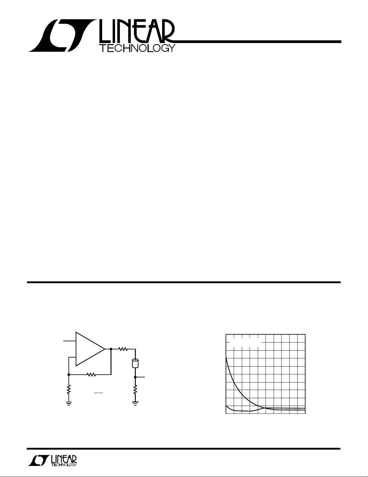
PPLICATITYPICAL
Video Cable Driver Differential Gain and Phase
vs Supply Voltage
0.20
V
IN
+
LT1227
–
RF
1k
RG
1k
V
OUT
V
IN
= 1
75Ω
75Ω
CABLE
V
OUT
75Ω
1227 TA01
NTSC COMPOSITE
f = 3.58MHz
0.16
0.12
0.08
DIFFERENTIAL PHASE (DEG)
0.04
0
5
∆φ
∆G
7
9
SUPPLY VOLTAGE (±V)
11
13
LT1227 • TA02
0.20
0.16
DIFFERENTIAL GAIN (%)
0.12
0.08
0.04
0
15
1
LT1227
A
W
O
LUTEXI T
S
A
WUW
ARB
U
G
I
S
Supply Voltage ..................................................... ±18V
Input Current ...................................................... ±15mA
Output Short Circuit Duration (Note 1) ........ Continuous
Operating Temperature Range
LT1227C.................................................. 0°C to 70°C
LT1227M ......................................... – 55°C to 125°C
Storage Temperature Range ................. –65°C to 150°C
Junction Temperature
Plastic Package ................................................ 150°C
Ceramic Package ............................................. 175°C
Lead Temperature (Soldering, 10 sec.)................ 300°C
/
TOP VIEW
= 175°C, θ
150°C, θ
TOP VIEW
S8 PACKAGE
150°C, θ
O
RDER I FOR ATIO
8
SHUTDOWN
+
7
V
6
OUT
NULL
N8 PACKAGE
8-LEAD PLASTIC DIP
100°C/W (J)
JA =
100°C/W (N)
JA =
8
SHUTDOWN
+
7
V
6
OUT
NULL
150°C/W
JA =
PACKAGE
1
NULL
2
–IN
3
+IN
–
V
45
J8 PACKAGE
8-LEAD CERAMIC DIP
T
JMAX
T
JMAX =
1
NULL
2
–IN
3
+IN
–
V
45
8-LEAD PLASTIC SO
T
JMAX =
Consult factory for Industrial grade parts.
WU
ORDER PART
NUMBER
LT1227MJ8
LT1227CN8
LT1227CS8
S8 PART MARKING
1227
U
LECTRICAL C CHARA TERIST
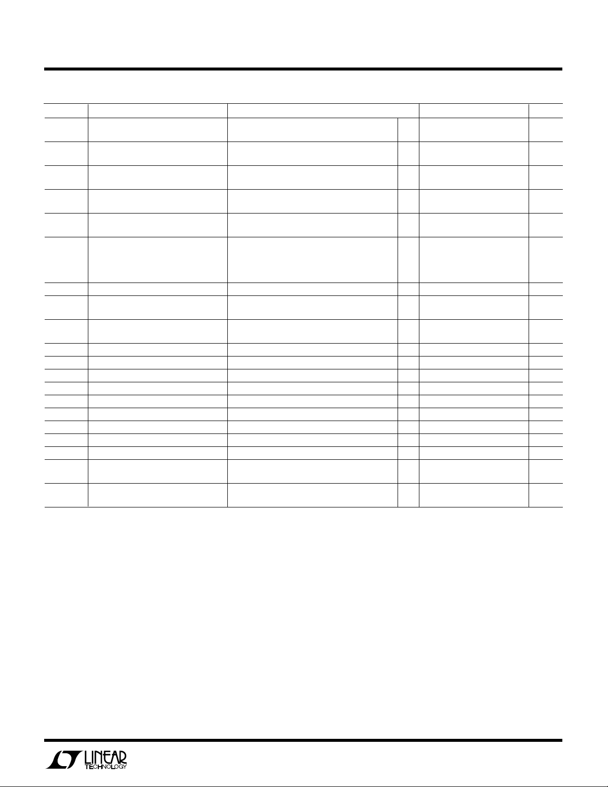
E
SYMBOL PARAMETER CONDITIONS MIN TYP MAX UNITS
V
OS
+ Noninverting Input Current T
I
IN
– Inverting Input Current T
I
IN
e
n
+i
n
–i
n
R
IN
C
IN
CMRR Common-Mode Rejection Ratio VS = ±15V, VCM = ±13V, TA = 25°C5562 dB
Input Offset Voltage TA = 25°C ±3 ±10 mV
Input Offset Voltage Drift ● 10 µV/°C
Input Noise Voltage Density f = 1kHz, RF = 1k, RG = 10Ω, RS = 0Ω 3.2 nV/√Hz
Noninverting Input Noise Current Density f = 1kHz 1.7 pA/√Hz
Inverting Input Noise Current Density f = 1kHz 32 pA/√Hz
Input Resistance VIN = ±13V, VS = ±15V ● 1.5 14 MΩ
Input Capacitance 3pF
Input Voltage Range VS = ±15V, TA = 25°C ±13 ±13.5 V
Inverting Input Current V
Common-Mode Rejection VS = ±15V, VCM = ±12V ● 10 µA/V
ICS
VCM = 0, ±5V ≤ VS ≤ ±15V, pulse tested, unless otherwise noted.
● ±15 mV
= 25°C ±0.3 ±3 µA
A
= 25°C ±10 ±60 µA
A
VIN = ±3V, VS = ±5V ● 1.5 11 MΩ
= ±5V, TA = 25°C ±3 ±3.5 V
V
S
= ±15V, VCM = ±12V ● 55 dB
V
S
= ±5V, VCM = ±3V, TA = 25°C5561dB
V
S
V
= ±5V, VCM = ±2V ● 55 dB
S
= ±15V, VCM = ±13V, TA = 25°C 3.5 10 µA/V
S
= ±5V, VCM = ±3V, TA = 25°C 4.5 10 µA/V
V
S
VS = ±5V, VCM = ±2V ● 10 µA/V
● ±10 µA
● ±100 µA
● ±12 V
● ±2V
2
LT1227
LECTRICAL C CHARA TERIST
E
SYMBOL PARAMETER CONDITIONS MIN TYP MAX UNITS
PSRR Power Supply Rejection Ratio VS = ±2V to ±15V, TA = 25°C6080dB
Noninverting Input Current VS = ±2V to ±15V, TA = 25°C250nA/V
Power Supply Rejection VS = ±3V to ±15V ● 50 nA/ V
Inverting Input Current VS = ±2V to ±15V, TA = 25°C 0.25 5 µA/V
Power Supply Rejection VS = ±3V to ±15V ● 5 µA/V
A
V
R
OL
V
OUT
I
OUT
I
S
I
8
SR Slew Rate (Notes 4 and 5) TA = 25°C 500 1100 V/µs
tr, t
f
BW Small-Signal Bandwidth VS = ±15V, RF = 1k, RG = 1k, RL = 150Ω 140 MHz
tr, t
f
t
S
Large-Signal Voltage Gain VS = ±15V, V
Transresistance, ∆V
Maximum Output Voltage Swing VS = ±15V, RL = 400Ω, TA = 25°C ±12 ±13.5 V
Maximum Output Current RL = 0Ω, TA = 25°C3060mA
Supply Current (Note 2) VS = ±15V, V
Positive Supply Current, Shutdown V
Shutdown Pin Current (Note 3) VS = ±15V ● 300 µA
Output Leakage Current, Shutdown VS = ±15V, Pin 8 Voltage = 0V, TA = 25°C10µA
Rise and Fall Time, V
Small-Signal Rise and Fall Time VS = ±15V, RF = 1k, RG = 1k, RL = 100Ω 3.3 ns
Propagation Delay VS = ±15V, RF = 1k, RG = 1k, RL = 100Ω 3.4 ns
Small-Signal Overshoot VS = ±15V, RF = 1k, RG = 1k, RL = 100Ω 5%
Settling Time 0.1%, V
Differential Gain (Note 6) VS = ±15V, RF = 1k, RG = 1k, RL = 150Ω 0.014 %
Differential Phase (Note 6) VS = ±15V, RF = 1k, RG = 1k, RL = 150Ω 0.010 DEG
OUT
OUT
/∆I
= 1V
– V
IN
P-P
ICS
V
S
VS = ±5V, V
S
VS = ±5V, V
VS = ±5V, RL = 150Ω, TA = 25°C ±3 ±3.7 V
S
VS = ±5V, RF = 1k, RG = 1k, RL = 150Ω 8.7 ns
VS = ±15V, RF = 1k, RG = 1k, RL = 1k 0.010 %
VS = ±15V, RF = 1k, RG = 1k, RL = 1k 0.013 DEG
VCM = 0, ±5V ≤ VS ≤ ±15V, pulse tested, unless otherwise noted.
= ±3V to ±15V ● 60 dB
= ±10V, RL = 1k ● 55 72 dB
OUT
= ±2V, RL = 150Ω ● 55 72 dB
OUT
= ±15V, V
= ±15V, Pin 8 Voltage = 0V, TA = 25°C 120 300 µA
= ±10V, RL = 1k ● 100 270 kΩ
OUT
= ±2V, RL = 150Ω ● 100 240 kΩ
OUT
● ±10 V
● ±2.5 V
= 0V, TA = 25°C 10 15.0 mA
OUT
= 10V, RF = 1k, RG = 1k, RL = 1k 50 ns
OUT
● 17.5 mA
● 500 µA
The ● denotes specifications which apply over the operating temperature
range.
Note 1: A heat sink may be required depending on the power supply
voltage.
Note 2: The supply current of the LT1227 has a negative temperature
coefficient. For more information, see Typical Performance Characteristics
curves.
Note 3: Ramp pin 8 voltage down from 15V while measuring I
drops to less than 0.5mA, measure pin 8 current.
. When I
S
S
Note 4: Slew rate is measured at ±5V on a ±10V output signal while
operating on ±15V supplies with RF = 2k, RG = 220Ω and RL = 400Ω.
Note 5: AC parameters are 100% tested on the ceramic and plastic DIP
package parts (J and N suffix) and are sample tested on every lot of the SO
packaged parts (S suffix).
Note 6: NTSC composite video with an output level of 2V.
3
LT1227
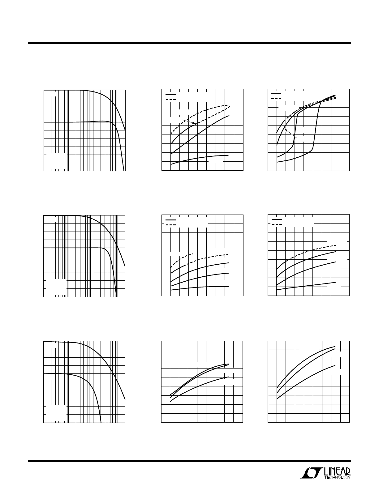
SUPPLY VOLTAGE (±V)
0
0
–3dB BANDWIDTH (MHz)
20
60
80
100
140
4
8
10 18
LT1227 • TPC06
40
160
180
120
26
12
14
16
PEAKING ≤ 0.5dB
PEAKING ≤ 5dB
RF = 500Ω
RF = 750Ω
RF = 2k
RF = 1k
SUPPLY VOLTAGE (±V)
0
0
–3dB BANDWIDTH (MHz)
2
6
8
10
14
4
8
10 18
LT1227 • TPC09
4
16
18
12
26
12
14
16
RF = 500Ω
RF = 2k
RF = 1k
LPER
F
O
R
ATYPICA
UW
CCHARA TERIST
E
C
ICS
Voltage Gain and Phase vs
Frequency, Gain = 6dB
10
PHASE
9
8
7
6
GAIN
5
4
VOLTAGE GAIN (dB)
3
2
VS = ±15V
= 100Ω
R
L
1
= 910Ω
R
F
0
0.1
1 10 100
FREQUENCY (MHz)
Voltage Gain and Phase vs
Frequency, Gain = 20dB
24
PHASE
23
22
21
20
GAIN
19
18
VOLTAGE GAIN (dB)
17
16
VS = ±15V
= 100Ω
R
L
15
= 825Ω
R
F
14
0.1
1 10 100
FREQUENCY (MHz)
LT1227 • TPC01
LT1227 • TPC04
0
PHASE SHIFT (DEG)
45
90
135
180
225
0
PHASE SHIFT (DEG)
45
90
135
180
225
–3dB Bandwidth vs Supply
Voltage, Gain = 2, RL = 100Ω
180
160
140
120
100
80
60
–3dB BANDWIDTH (MHz)
40
20
0
PEAKING ≤ 0.5dB
PEAKING ≤ 5dB
RF = 500Ω
RF = 750Ω
0
26
4
SUPPLY VOLTAGE (±V)
10 18
8
–3dB Bandwidth vs Supply
Voltage, Gain = 10, RL = 100Ω
180
160
140
120
100
80
60
–3dB BANDWIDTH (MHz)
40
20
0
PEAKING ≤ 0.5dB
PEAKING ≤ 5dB
RF = 250Ω
0
4
26
SUPPLY VOLTAGE (±V)
10 18
8
RF = 1k
RF = 2k
14
12
RF = 500Ω
RF = 750Ω
RF = 1k
RF = 2k
14
12
16
LT1227 • TPC02
16
LT1227 • TPC05
–3dB Bandwidth vs Supply
Voltage, Gain = 2, RL = 1k
180
160
140
120
100
80
60
–3dB BANDWIDTH (MHz)
40
20
0
PEAKING ≤ 0.5dB
PEAKING ≤ 5dB
RF = 750Ω
0
26
4
SUPPLY VOLTAGE (±V)
RF = 1.5k
RF = 1k
8
–3dB Bandwidth vs Supply
Voltage, Gain = 10, RL = 1k
= 2k
R
F
14
10 18
12
16
LT1227 • TPC03
44
43
42
41
40
39
38
VOLTAGE GAIN (dB)
37
36
35
34
0.1
4
Voltage Gain and Phase vs
Frequency, Gain = 40dB
PHASE
GAIN
VS = ±15V
= 100Ω
R
L
= 500Ω
R
F
1 10 100
FREQUENCY (MHz)
LT1227 • TPC07
0
PHASE SHIFT (DEG)
45
90
135
180
225
–3dB Bandwidth vs Supply
Voltage, Gain = 100, RL = 100Ω
18
16
14
12
10
8
6
–3dB BANDWIDTH (MHz)
4
2
0
0
26
RF = 500Ω
4
SUPPLY VOLTAGE (±V)
10 18
8
12
RF = 1k
RF = 2k
14
16
LT1227 • TPC08
–3dB Bandwidth vs Supply
Voltage, Gain = 100, RL = 1k
 Loading...