

Linear Technology LT1224 Datasheet
LT1224
Very High Speed
Operational Amplifier
EATU
F
■
Unity-Gain Stable
■
45MHz Gain-Bandwidth
■
400V/µs Slew Rate
■
7V/mV DC Gain: RL = 500Ω
■
Maximum Input Offset Voltage: 2mV
■
±12V Minimum Output Swing into 500Ω
■
Wide Supply Range: ±2.5V to ±15V
■
7mA Supply Current
■
90ns Settling Time to 0.1%, 10V Step
■
Drives All Capacitive Loads
PPLICATI
A
■
Wideband Amplifiers
■
Buffers
■
Active Filters
■
Video and RF Amplification
■
Cable Drivers
■
Data Acquisition Systems
RE
S
O
U
S
DUESCRIPTIO
The LT1224 is a very high speed operational amplifier with
excellent DC performance. The LT1224 features reduced
input offset voltage and higher DC gain than devices with
comparable bandwidth and slew rate. The circuit is a
single gain stage with outstanding settling characteristics.
The fast settling time makes the circuit an ideal choice for
data acquisition systems. The output is capable of driving
a 500Ω load to ±12V with ± 15V supplies and a 150Ω load
to ±3V on ±5V supplies. The circuit is also capable of
driving large capacitive loads which makes it useful in
buffer or cable driver applications.
The LT1224 is a member of a family of fast, high performance amplifiers that employ Linear Technology
Corporation’s advanced bipolar complementary
processing.
U
O
A
PPLICATITYPICAL
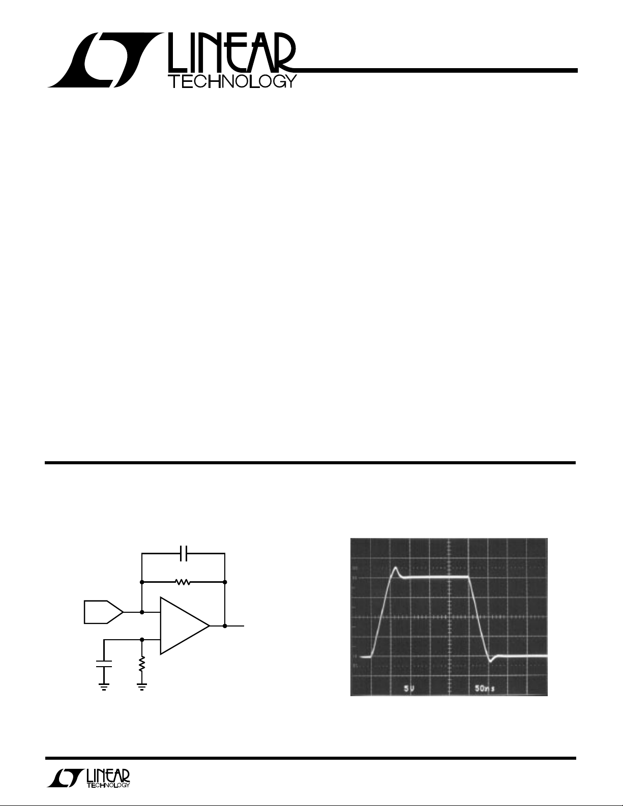
DAC Current-to-Voltage Converter Inverter Pulse Response
7pF
5k
DAC-08
TYPE
0.1µF 5k 1 LSB SETTLING = 140ns
–
+
LT1224
V
OUT
LT1224 • TA01
LT1224 • TA02
1
LT1224
WU
U
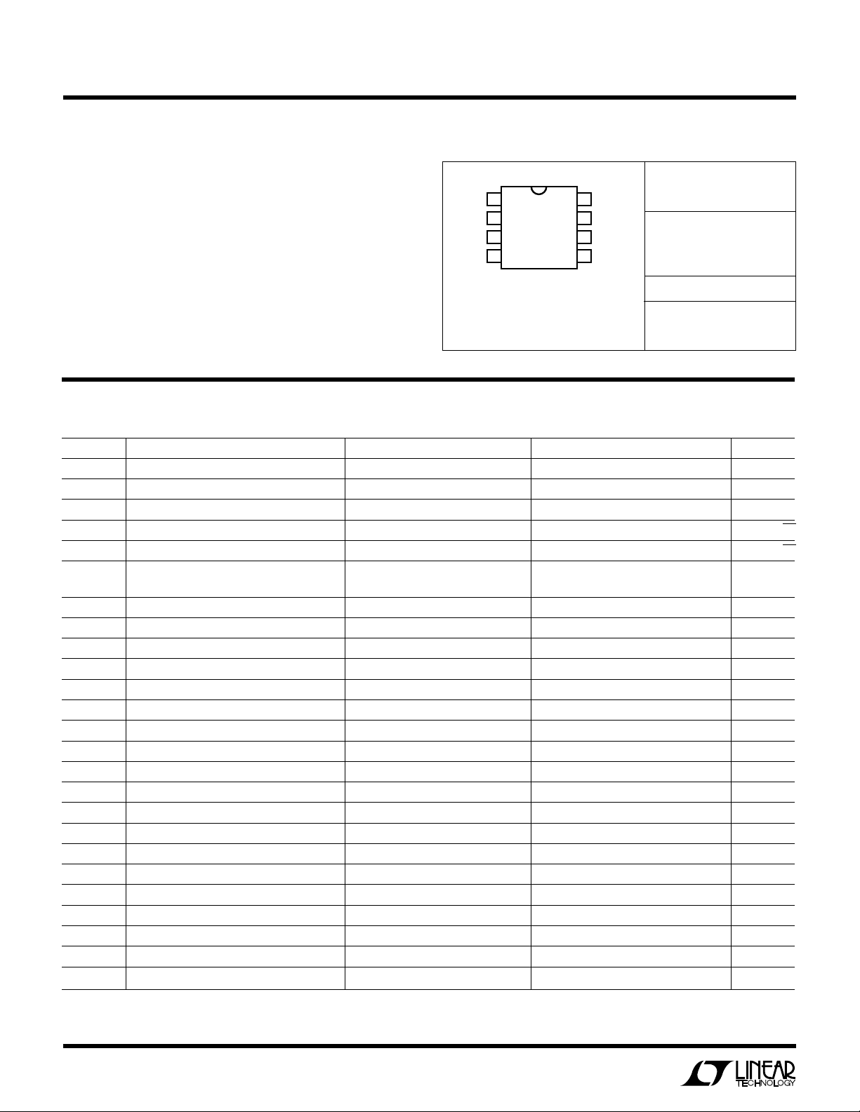
PACKAGE
/
O
RDER I FOR ATIO
W
O
A
LUTEXI T
S
Total Supply Voltage (V+ to V–) ............................... 36V
Differential Input Voltage .........................................±6V
Input Voltage ............................................................±V
Output Short Circuit Duration (Note 1) ............Indefinite
Operating Temperature Range
LT1224C................................................ 0°C to 70°C
Maximum Junction Temperature
Plastic Package .............................................. 150°C
Storage Temperature Range ................. – 65°C to 150°C
A
WUW
ARB
U
G
I
S
S
TOP VIEW
1NULL
2
–IN
+IN
3
–
V
N8 PACKAGE
8-LEAD PLASTIC DIP
T
= 150°C, θJA = 100°C/W (N8)
JMAX
T
= 150°C, θJA = 150°C/W (S8)
JMAX
NULL
8
+
7
V
6
OUT
54
NC
S8 PACKAGE
8-LEAD PLASTIC SOIC
LT1224 • POI01
ORDER PART
NUMBER
LT1224CN8
LT1224CS8
S8 PART MARKING
1224
Lead Temperature (Soldering, 10 sec.)................. 300°C
LECTRICAL C CHARA TERIST
E
SYMBOL PARAMETER CONDITIONS MIN TYP MAX UNITS
V
OS
I
OS
I
B
e
n
i
n
R
IN
C
IN
CMRR Common-Mode Rejection Ratio VCM = ±12V 86 100 dB
PSRR Power Supply Rejection Ratio VS = ±5V to ±15V 75 84 dB
A
VOL
V
OUT
I
OUT
SR Slew Rate A
GBW Gain-Bandwidth f = 1MHz 45 MHz
tr, t
f
t
s
R
O
I
S
Input Offset Voltage (Note 2) 0.5 2.0 mV
Input Offset Current 100 400 nA
Input Bias Current 48 µA
Input Noise Voltage f = 10kHz 22 nV/√Hz
Input Noise Current f = 10kHz 1.5 pA/√Hz
Input Resistance VCM = ±12V 24 40 MΩ
Input Capacitance 2pF
Input Voltage Range
Input Voltage Range
Large-Signal Voltage Gain V
Output Swing RL = 500Ω±12.0 ±13.3 V
Output Current V
Full Power Bandwidth 10V Peak, (Note 4) 6.4 MHz
Rise Time, Fall Time A
Overshoot A
Propagation Delay 50% VIN to 50% V
Settling Time 10V Step, 0.1% 90 ns
Differential Gain f = 3.58MHz, RL = 150Ω 1%
Differential Phase f = 3.58MHz, RL = 150Ω 2.4 Deg
Output Resistance A
Supply Current 79 mA
+
–
ICS
VS = ±15V, TA = 25°C, RL = 1k, VCM = 0V unless otherwise noted.
Differential 250 kΩ
12 14 V
–13 –12 V
= ±10V, RL = 500Ω 3.3 7 V/mV
OUT
= ±12V 24 40 mA
OUT
= –2, (Note 3) 250 400 V/µs
VCL
= 1, 10% to 90%, 0.1V 5 ns
VCL
= 1, 0.1V 30 %
VCL
OUT
= 1, f = 1MHz 2.5 Ω
VCL
5ns
2
LT1224
LECTRICAL C CHARA TERIST
E
SYMBOL PARAMETER CONDITIONS MIN TYP MAX UNITS
V
OS
I
OS
I
B
CMRR Common-Mode Rejection Ratio VCM = ±2.5V 86 98 dB
A
VOL
V
OUT
I
OUT
SR Slew Rate A
GBW Gain-Bandwidth f = 1MHz 34 MHz
tr, t
f
t
s
I
S
Input Offset Voltage (Note 2) 1 4 mV
Input Offset Current 100 400 nA
Input Bias Current 48 µA
Input Voltage Range
Input Voltage Range
Large-Signal Voltage Gain V
Output Swing RL = 500Ω±3.0 ±3.7 V
Output Current V
Full Power Bandwidth 3V Peak, (Note 4) 13.3 MHz
Rise Time, Fall Time A
Overshoot A
Propagation Delay 50% VIN to 50% V
Settling Time –2.5V to 2.5V, 0.1% 90 ns
Supply Current 79 mA
+
–
ICS
VS = ±5V, TA = 25°C, RL = 1k, VCM = 0V unless otherwise noted.
2.5 4 V
–3 – 2.5 V
= ±2.5V, RL = 500Ω 2.5 7 V/mV
OUT
= ±2.5V, RL = 150Ω 3 V/mV
V
OUT
= 150Ω±3.0 ±3.3 V
R
L
= ±3V 20 40 mA
OUT
= –2, (Note 3) 250 V/µs
VCL
= 1, 10% to 90%, 0.1V 7 ns
VCL
= 1, 0.1V 20 %
VCL
OUT
7ns
LECTRICAL C CHARA TERIST
E
SYMBOL PARAMETER CONDITIONS MIN TYP MAX UNITS
V
OS
I
OS
I
B
CMRR Common-Mode Rejection Ratio VS = ±15V, VCM = ±12V and VS = ±5V, VCM = ±2.5V 83 98 dB
PSRR Power Supply Rejection Ratio VS = ±5V to ±15V 73 84 dB
A
VOL
V
OUT
I
OUT
SR Slew Rate VS = ±15V, A
I
S
Note 1: A heat sink may be required to keep the junction temperature
below absolute maximum when the output is shorted indefinitely.
Note 2: Input offset voltage is tested with automated test equipment
in <1 second.
Input Offset Voltage VS = ±15V, (Note 2) 1 4 mV
VS = ±5V, (Note 2) 2 5 mV
Input V
Input Offset Current VS = ±15V and VS = ±5V 100 600 nA
Input Bias Current VS = ±15V and VS = ±5V 4 9 µA
Large-Signal Voltage Gain VS = ±15V, V
Output Swing VS = ±15V, RL = 500Ω±12.0 ±13.3 V
Output Current VS = ±15V, V
Supply Current VS = ±15V and VS = ±5V 7 10.5 mA
Drift 25 µV/°C
OS
= ±5V, V
V
S
VS = ±5V, RL = 500Ω or 150Ω±3.0 ±3.3 V
= ±5V, V
V
S
0°C ≤ TA ≤ 70°C, RL = 1k, VCM = 0V unless otherwise noted.
ICS
= ±10V, RL = 500Ω 2.5 7 V/mV
OUT
= ±2.5V, RL = 500Ω 2.0 7 V/mV
OUT
= ±12V 24 40 mA
OUT
= ±3V 20 40 mA
OUT
= –2, (Note 3) 250 400 V/µs
VCL
Note 3: Slew rate is measured in a gain of –2 between ±10V on the output
with ±6V on the input for ±15V supplies and ±2V on the output with
±1.75V on the input for ±5V supplies.
Note 4: Full power bandwidth is calculated from the slew rate
measurement: FPBW = SR/2πVp.
3
 Loading...