

Linear Technology LT1223 Datasheet
LT1223
100MHz Current
Feedback Amplifier
EATU
F
■
100MHz Bandwidth at AV = 1
■
1000V/µs Slew Rate
■
Wide Supply Range: ±5V to ±15V
■
1mV Input Offset Voltage
■
1µA Input Bias Current
■
5MΩ Input Resistance
■
75ns Settling Time to 0.1%
■
50mA Output Current
■
6mA Quiescent Current
PPLICATI
A
■
Video Amplifiers
■
Buffers
■
IF and RF Amplification
■
Cable Drivers
■
8-, 10-, 12-Bit Data Acquisition Systems
RE
S
O
U
S
DUESCRIPTIO
The LT1223 is a 100MHz current feedback amplifier with
very good DC characteristics. The LT1223’s high slew
rate, 1000V/µs, wide supply range, ±15V, and large output
drive, ±50mA, make it ideal for driving analog signals over
double- terminated cables. The current feedback amplifier
has high gain bandwidth at high gains, unlike conventional
op amps.
The LT1223 comes in the industry standard pinout and
can upgrade the performance of many older products.
The LT1223 is manufactured on Linear Technology’s
proprietary complementary bipolar process.
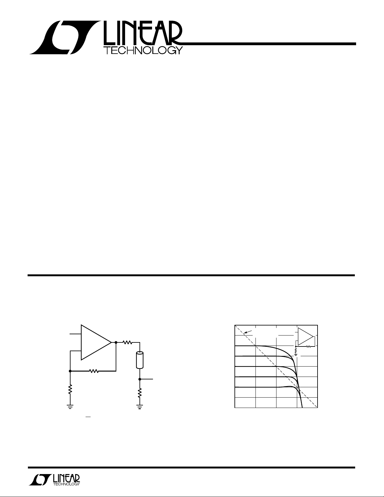
CA
A
PPLICATITYPI
L
V
+
IN
LT1223
–
RG
1k
RF
A = 1 +
V
R
AT AMPLIFIER OUTPUT.
6dB LESS AT V .
U
O
Video Cable Driver Voltage Gain vs Frequency
60
Ω
75
75
R
F
1k
G
OUT
Ω
CABLE
Ω
75
LT1223 • TA02
V
OUT
50
40
30
20
10
VOLTAGE GAIN (dB)
0
–10
–20
100k
RG = 10
R
= 33
G
= 110
R
G
R
= 470
G
R
= ∞
G
100MHz GAIN
BANDWIDTH
1M
10M 100M 1G
FREQUENCY (Hz)
+
–
1k
R
G
LT1223 • TPC01
1
LT1223
WU
U
PACKAGE
/
O
RDER I FOR ATIO
W
O
A
LUTEXI T
S
Supply Voltage ...................................................... ±18V
Differential Input Voltage ......................................... ±5V
Input Voltage ............................ Equal to Supply Voltage
Output Short Circuit Duration (Note 1) .........Continuous
Operating Temperature Range
LT1223M........................................ –55°C to 125°C
LT1223C................................................ 0°C to 70°C
Storage Temperature Range ................. –65°C to 150°C
Junction Temperature Plastic Package...........150°C
Junction Temperature Ceramic Package ........ 175°C
Lead Temperature (Soldering, 10 sec.)................. 300°C
LECTRICAL C CHARA TERIST
E
SYMBOL PARAMETER CONDITIONS MIN TYP MAX UNITS
V
OS
I
+ Noninverting Input Current VCM = 0V ±1 ±3 µA
IN
IIN– Inverting Input Current VCM = 0V ±1 ±3 µA
e
n
i
n
R
IN
C
IN
CMRR Common-Mode Rejection Ratio VCM = ±10V 56 63 dB
PSRR Power Supply Rejection Ratio VS = ±4.5V to ±18V 68 80 dB
A
V
R
OL
V
OUT
I
OUT
SR Slew Rate RF = 1.5k, RG = 1.5k, (Note 2) 800 1300 V/µs
BW Bandwidth RF = 1k, RG = 1k, V
t
r
t
PD
t
s
R
OUT
I
S
Input Offset Voltage VCM = 0V ±1 ±3mV
Input Noise Voltage Density f = 1kHz, RF = 1k, RG = 10Ω 3.3 nV/√Hz
Input Noise Current Density f = 1kHz, RF = 1k, RG = 10Ω 2.2 pA/√Hz
Input Resistance VIN = ±10V 1 10 MΩ
Input Capacitance 1.5 pF
Input Voltage Range ±10 ±12 V
Inverting Input Current Common-Mode Rejection VCM = ±10V 30 100 nA/ V
Noninverting Input Current Power Supply Rejection VS = ±4.5V to ±18V 12 100 nA/V
Inverting Input Current Power Supply Rejection VS = ±4.5V to ±18V 60 500 nA/V
Large Signal Voltage Gain R
Transresistance, ∆V
Maximum Output Voltage Swing R
Maximum Output Current R
Rise Time RF = 1.5k, RG = 1.5k, V
Propagation Delay RF = 1.5k, RG = 1.5k, V
Overshoot RF = 1.5k, RG = 1.5k, V
Settling Time, 0.1% RF = 1k, RG = 1k, V
Differential Gain RF = 1k, RG = 1k, RL = 150Ω 0.02 %
Differential Phase RF = 1k, RG = 1k, RL = 150Ω 0.12 Deg
Open-Loop Output Resistance V
Supply Current VIN = 0V 6 10 mA
Supply Current, Shutdown Pin 8 Current = 200µA24mA
A
WUW
ARB
/∆IIN–R
OUT
U
G
S
I
1NULL
2
–IN
+IN
3
–
V
J8 PACKAGE
8-LEAD CERAMIC DIP
8-LEAD PLASTIC SOIC
T
= 175°C, θJA = 100°C/W(J8)
J MAX
T
= 150°C, θJA = 100°C/W(N8)
J MAX
T
= 150°C, θJA = 150°C/W(S8)
J MAX
VS = ±15V, TA = 25°C, unless otherwise noted.
ICS
= 400Ω, V
LOAD
= 400Ω, V
LOAD
= 200Ω±10 ±12 V
LOAD
= 200Ω 50 60 mA
LOAD
= 0, I
OUT
OUT
= ±10V 70 89 dB
OUT
= ±10V 1.5 5 MΩ
OUT
= 100mV 100 MHz
OUT
OUT
OUT
OUT
= 10V 75 ns
OUT
= 0 35 Ω
TOP VIEW
SHUTDOWN
8
+
7
V
6
OUT
54
NULL
N8 PACKAGE
8-LEAD PLASTIC DIP
S8 PACKAGE
LT1223 • POI01
LT1223M/C
= 1V 6.0 ns
= 1V 6.0 ns
= 1V 5 %
ORDER PART
NUMBER
LT1223MJ8
LT1223CJ8
LT1223CN8
LT1223CS8
S8 PART MARKING
1223
2
LT1223
LECTRICAL C CHARA TERIST
E
SYMBOL PARAMETER CONDITIONS MIN TYP MAX UNITS
V
OS
I
+ Noninverting Input Current VCM = 0V ● ±1 ±3 µA
IN
IIN– Inverting Input Current VCM = 0V ● ±1 ±3 µA
R
IN
CMRR Common-Mode Rejection Ratio VCM = ±10V ● 56 63 dB
PSRR Power Supply Rejection Ratio VS = ±4.5V to ±18V ● 68 80 dB
A
V
R
OL
V
OUT
I
OUT
I
S
Input Offset Voltage VCM = 0V ● ±1 ±3mV
Input Resistance VIN = ±10V ● 110 MΩ
Input Voltage Range ● ±10 ±12 V
Inverting Input Current Common-Mode Rejection VCM = ±10V ● 30 100 nA/V
Noninverting Input Current Power Supply Rejection VS = ±4.5V to ±18V ● 12 100 nA/V
Inverting Input Current Power Supply Rejection VS = ±4.5V to ±18V ● 60 500 nA/ V
Large-Signal Voltage Gain R
Transresistance, ∆V
Maximum Output Voltage Swing R
Maximum Output Current R
Supply Current VIN = 0V ● 610 mA
Supply Current, Shutdown Pin 8 Current = 200µA ● 24 mA
/∆IIN–R
OUT
VS = ±15V, VCM = 0V, 0°C ≤ TA ≤ 70°C, unless otherwise noted.
ICS
= 400Ω, V
LOAD
= 400Ω, V
LOAD
= 200Ω ● ±10 ±12 V
LOAD
= 200Ω ● 50 60 mA
LOAD
= ±10V ● 70 89 dB
OUT
= ±10V ● 1.5 5 MΩ
OUT
LT1223C
LECTRICAL C CHARA TERIST
E
SYMBOL PARAMETER CONDITIONS MIN TYP MAX UNITS
V
OS
I
+ Noninverting Input Current VCM = 0V ● ±1 ±5 µA
IN
IIN– Inverting Input Current VCM = 0V ● ±1 ±10 µA
R
IN
CMRR Common-Mode Rejection Ratio VCM = ±10V ● 56 63 dB
PSRR Power Supply Rejection Ratio VS = ±4.5V to ±15V ● 68 80 dB
A
V
R
OL
V
OUT
I
OUT
I
S
● denotes the specifications which apply over the full operating
The
temperature range.
Note 1: A heat sink may be required.
Note 2: Noninverting operation, V
Input Offset Voltage VCM = 0V ● ±1 ±5mV
Input Resistance VIN = ±10V ● 110 MΩ
Input Voltage Range ● ±10 ±12 V
Inverting Input Current Common-Mode Rejection VCM = ±10V ● 30 100 nA/V
Noninverting Input Current Power Supply Rejection VS = ±4.5V to ±15V ● 12 200 nA/V
Inverting Input Current Power Supply Rejection VS = ±4.5V to ±15V ● 60 500 nA/V
Large-Signal Voltage Gain R
Transresistance, ∆V
Maximum Output Voltage Swing R
Maximum Output Current R
Supply Current VIN = 0V ● 610 mA
Supply Current, Shutdown Pin 8 Current = 200µA ● 24 mA
/∆IIN–R
OUT
= ±10V, measured at ±5V.
OUT
VS = ±15V, VCM = 0V, –55°C ≤ TA ≤ 125°C, unless otherwise noted.
ICS
LT1223M
= 400Ω, V
LOAD
= 400Ω, V
LOAD
= 200Ω ● ±7 ±12 V
LOAD
= 200Ω ● 35 60 mA
LOAD
= ±10V ● 70 89 dB
OUT
= ±10V ● 1.5 5 MΩ
OUT
3
LT1223
COMMON MODE VOLTAGE (V)
–15
–10
–l ( A)
–6
–2
2
6
10
LT1223 • TPC07
–10 –5 0 5 10 15
125°C
µ
–8
–4
0
4
8
–55°C
±V = 15V
S
25°C
B
CASE TEMPERATURE (°C)
–50
0
OUTPUT SHORT CIRCUIT CURRENT (mA)
30
100
LT1223 • TPC04
–25 0 25 50 75 100 125
10
20
40
50
60
70
80
90
SUPPLY VOLTAGE ( V)
0
–20
OUTPUT VOLTAGE SWING (V)
–10
–5
10
20
LT1223 • TPC10
2 4 6 8 101214161820
±
125°C
–15
0
5
15
25°C
25°C
125°C
–55°C
–55°C
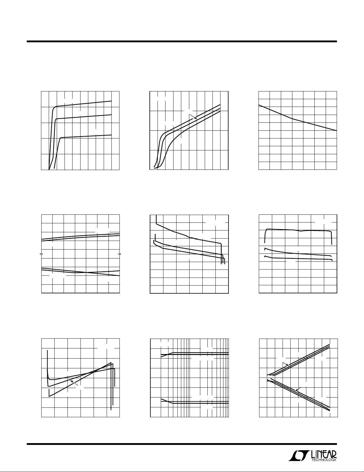
UW
Y
PICA
10
8
6
4
SUPPLY CURRENT (mA)
2
LPER
F
O
R
AT
CCHARA TERIST
E
C
ICS
Supply Current vs Supply Voltage, Supply Current vs Supply Voltage Output Short Circuit-Current vs
VIN = 0 (Operating) (Shutdown) Temperature
4
125°C
25°C
–55°C
PIN 8 = 0V
3
125°C
2
SUPPLY CURRENT (mA)
1
25°C
–55°C
0
2 4 6 8 101214161820
0
SUPPLY VOLTAGE ( V)
Input Common-Mode Limit vs
Temperature +IB vs Common-Mode Voltage –IB vs Common-Mode Voltage
V+
–1
–2
–3
V = 5V
S
–4
+4
+3
V = –15V
+2
COMMON MODE RANGE (V)
S
+1
V–
–50 –25 0 25 50 75 100 125
TEMPERATURE (°C)
VOS vs Common-Mode Voltage Load Resistor Supply Voltage
20
15
10
5
0
OS
V (mV)
–5
–10
–15
–20
–15
4
125°C
–55°C
–10 –5 0 5 10 15
COMMON MODE VOLTAGE (V)
25°C
±
LT1223 • TPC02
V = 15V
S
V = –5V
S
LT1223 • TPC05
V = 15V
S
LT1223 • TPC08
0
2 4 6 8 101214161820
0
±
–55°C
LT1223 • TPC03
V = ±15V
S
LT1223 • TPC06
5
4
3
2
1
µ
0
B
+l ( A)
–1
–2
–3
–4
–5
–15
SUPPLY VOLTAGE ( V)
25°C
125°C
–10 –5 0 5 10 15
COMMON MODE VOLTAGE (V)
Output Voltage Swing vs Output Voltage Swing vs
20
±
V = 15VS±
15
10
5
0
–5
–10
OUTPUT VOLTAGE SWING (V)
–15
–20
100
LOAD RESISTOR ( )
125°C
25°C, –55°C
25°C, –55°C
125°C
1000 10000
Ω
LT1223 • TPC09
 Loading...