

Linear Technology LT1216, LT1215 Datasheet
FEATURES
■
Slew Rate: 50V/µs Typ
■
Gain-Bandwidth Product: 23MHz Typ
■
Fast Settling to 0.01%
2V Step to 200µV: 250ns Typ
10V Step to 1mV: 480ns Typ
■
Excellent DC Precision in All Packages
Input Offset Voltage: 450µV Max
Input Offset Voltage Drift: 10µV/°C Max
Input Offset Current: 120nA Max
Input Bias Current: 600nA Max
Open-Loop Gain: 1000V/mV Min
■
Single Supply Operation
Input Voltage Range Includes Ground
Output Swings to Ground While Sinking Current
■
Low Input Noise Voltage: 12.5nV/√Hz Typ
■
Low Input Noise Current: 0.5pA/√Hz Typ
■
Specified on 3.3V, 5V and ±15V
■
Large Output Drive Current: 30mA Min
■
Low Supply Current per Amplifier: 6.6mA Max
■
Dual in 8-Pin DIP and SO-8
■
Quad in 14-Pin DIP and NARROW SO-16
Note: For applications requiring less slew rate, see the LT1211/LT1212 and
LT1213/LT1214 data sheets.
LT1215/LT1216
23MHz, 50V/µs, Single Supply
Dual and Quad
Precision Op Amps
U
DESCRIPTIO
The LT®1215 is a dual, single supply precision op amp with
a 23MHz gain-bandwidth product and a 50V/µs slew rate.
The LT1216 is a quad version of the same amplifier. The
DC precision of the LT1215/LT1216 eliminates trims in
most systems while providing high frequency performance not usually found in single supply amplifiers.
The LT1215/LT1216 will operate on any supply greater
than 2.5V and less than 36V total. These amplifiers are
specified on single 3.3V, single 5V and ±15V supplies, and
only require 5mA of quiescent supply current per amplifier. The inputs can be driven beyond the supplies without
damage or phase reversal of the output. The minimum
output drive is 30mA, ideal for driving low impedance
loads.
U
APPLICATIO S
■
2.5V Full-Scale 12-Bit Systems: VOS ≤ 0.75 LSB
■
10V Full-Scale 16-Bit Systems: VOS ≤ 3 LSB
■
Active Filters
■
Photo Diode Amplifiers
■
DAC Current to Voltage Amplifiers
■
Battery-Powered Systems
, LTC and LT are registered trademarks of Linear Technology Corporation.
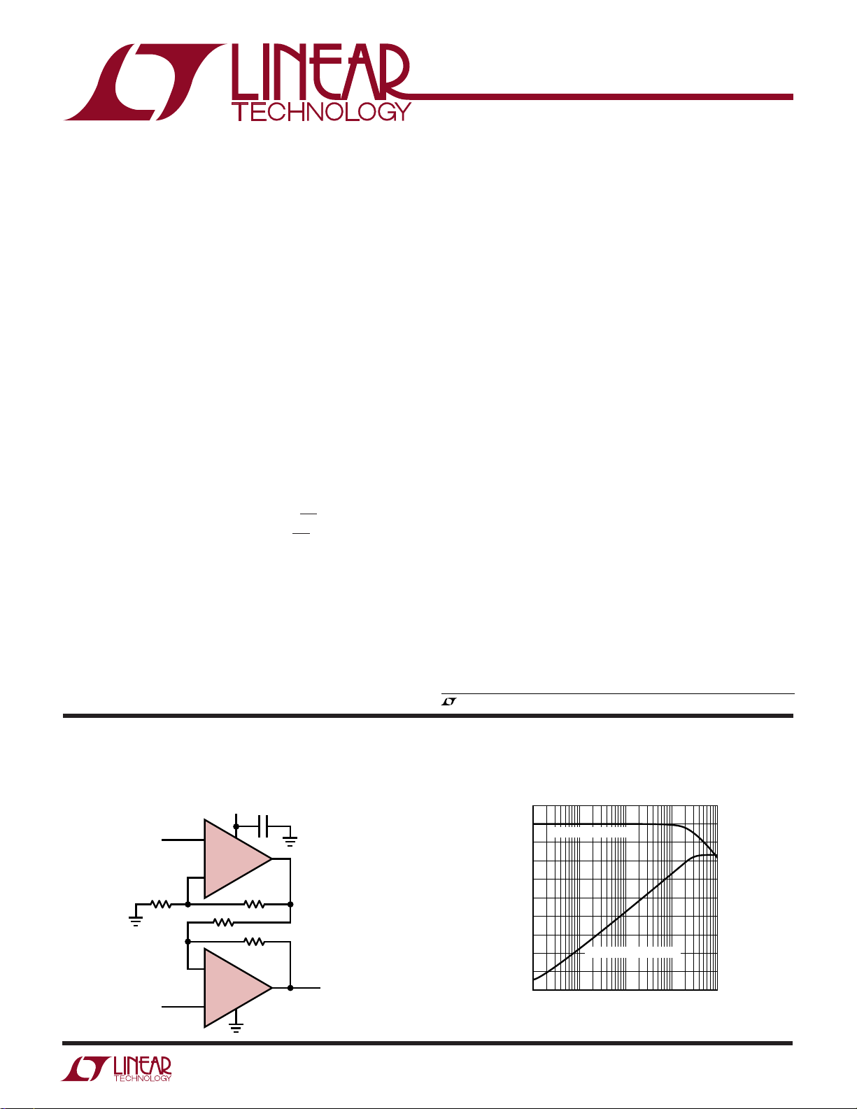
TYPICAL APPLICATIO
Single Supply Instrumentation Amplifier
5V
0.1µF
–
V
IN
V
IN
1020Ω
+
+
LT1215
–
113Ω
–
LT1215
+
1/2
113Ω
1020Ω
1/2
U
NOTE:
0.1% RESISTORS GIVE CMRR ≥ 68dB.
GAIN IS 10.0V/V.
COMMON MODE INPUT RANGE
IS FROM 0.3V TO 3.0V.
BANDWIDTH IS 2.8MHz.
V
OUT
1215/16 TA01
Frequency Response
30
20
DIFFERENTIAL INPUT
10
0
–10
–20
GAIN (dB)
–30
–40
–50
–60
–70
1k 100k 1M 10M
COMMON MODE INPUT
10k
FREQUENCY (Hz)
1215/16 TA02
1
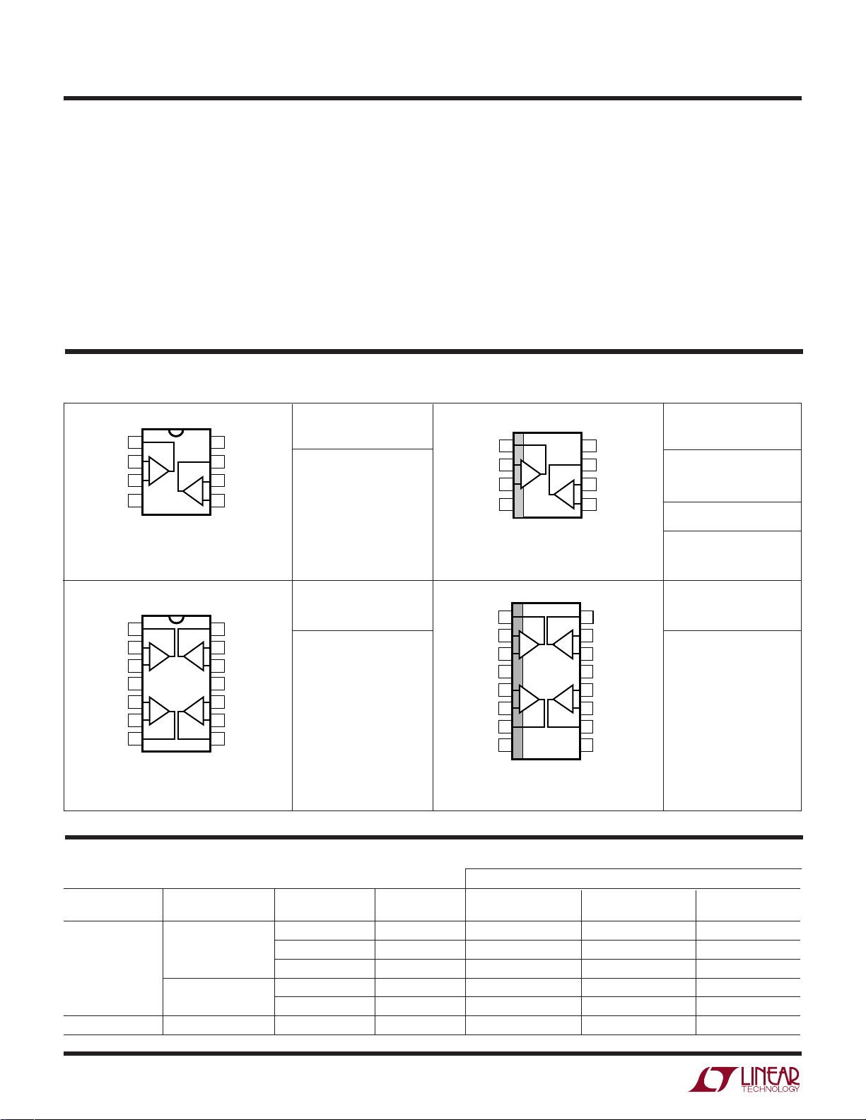
LT1215/LT1216
1
2
3
4
8
7
6
5
TOP VIEW
S8 PACKAGE
8-LEAD PLASTIC SO
B
A
OUT A
–IN A
+IN A
V
–
V
+
OUT B
–IN B
+IN B
TOP VIEW
S PACKAGE
16-LEAD PLASTIC SO
1
2
3
4
5
6
7
8
16
15
14
13
12
11
10
9
OUT A
–IN A
+IN A
V
+
+IN B
–IN B
OUT B
NC
OUT D
–IN D
+IN D
V
–
+IN C
–IN C
OUT C
NC
A
C
B
D
N PACKAGE
14-LEAD PDIP
OUT A
–IN A
+IN A
V
+
+IN B
–IN B
OUT B
OUT D
–IN D
+IN D
V
–
+IN C
–IN C
OUT C
1
2
3
4
5
6
7
14
13
12
11
10
9
8
D
A
C
B
TOP VIEW
A
W
O
LUTEXI TIS
S
A
WUW
U
ARB
G
Total Supply Voltage (V+ to V–) ............................. 36V
Input Current ..................................................... ±15mA
Output Short-Circuit Duration (Note 2)........ Continuous
Operating Temperature Range
LT1215C/LT1216C (Note 3) .............. –40°C to 85°C
LT1215M ......................................... –55°C to 125°C
Specified Temperature Range
LT1215C/LT1216C (Note 4) .............. –40°C to 85°C
LT1215M ......................................... –55°C to 125°C
WU
/
PACKAGE
OUT A
–IN A
+IN A
–
V
J8 PACKAGE
8-LEAD CERDIP
T
JMAX
T
JMAX
O
RDER I FOR ATIO
TOP VIEW
1
2
A
3
4
= 175°C, θJA = 100°C/W (J)
= 150°C, θJA = 100°C/W (N)
8
V
7
OUT B
6
–IN B
B
5
+IN B
N8 PACKAGE
8-LEAD PDIP
ORDER PART
+
NUMBER
LT1215CN8
LT1215ACN8
LT1215MJ8
LT1215AMJ8
(Note 1)
Storage Temperature Range ................ –65°C to 150°C
Junction Temperature (Note 5).............................150°C
Plastic Package (CN8, CS8, CN, CS)................ 150°C
Ceramic Package (MJ8) .................................. 175°C
Lead Temperature (Soldering, 10 sec)................. 300°C
U
ORDER PART
NUMBER
LT1215CS8
S8 PART MARKING
T
= 150°C, θJA = 150°C/W
JMAX
1215
ORDER PART
NUMBER
LT1216CS
T
= 150°C, θJA = 70°C/W
JMAX
ORDER PART
NUMBER
LT1216CN
T
= 150°C, θJA = 100°C/W
JMAX
U
AVAILABLE OPTIO S
NUMBER OF MAX TC V
OP AMPS T
Two (Dual) –40°C to 85°C 300µV2.5µV/°C LT1215ACN8
2
Four (Quad) –40°C to 85°C 450µV10µV/°C LT1216CN LT1216CS
RANGE MAX VOS (25°C) (∆VOS/∆T) (J) (N) (S)
A
450µV5µV/°C LT1215CN8
450µV10µV/°C LT1215CS8
–55°C to 125°C 300µV2.5µV/°C LT1215AMJ8
450µV5µV/°C LT1215MJ8
OS
CERAMIC PLASTIC DIP SURFACE MOUNT
PACKAGE
LT1215/LT1216
LECTRICAL C CHARA TERIST
E
5V
VS = 5V, VCM = 0.5V, V
SYMBOL PARAMETER CONDITIONS MIN TYP MAX MIN TYP MAX UNITS
V
OS
∆V
∆Time
I
OS
I
B
e
n
i
n
CMRR Common Mode Rejection Ratio VCM = 0V to 3V 90 108 86 108 dB
PSRR Power Supply Rejection Ratio VS = 2.5V to 12.5V 96 115 93 115 dB
A
VOL
I
O
SR Slew Rate AV = –2 30 30 V/µs
GBW Gain-Bandwidth Product f = 100kHz 23 23 MHz
I
S
tr, t
OS Overshoot AV = 1, VO = 100mV 25 25 %
t
PD
t
S
THD Total Harmonic Distortion AV = 1, VO = 1V
Input Offset Voltage 125 300 150 450 µV
Long-Term Input Offset 0.8 1.0 µV/Mo
OS
Voltage Stability
Input Offset Current 35 80 35 120 nA
Input Bias Current 420 500 420 600 nA
Input Noise Voltage 0.1Hz to 10Hz 400 400 nV
Input Noise Voltage Density fO = 10Hz 15.0 15.0 nV/√Hz
Input Noise Current Density fO = 10Hz 7.0 7.0 pA/√Hz
Input Resistance (Note 6) Differential Mode 10 40 10 40 MΩ
Input Capacitance f = 1MHz 10 10 pF
Input Voltage Range 3.0 3.2 3.0 3.2 V
Large-Signal Voltage Gain VO = 0.05V to 3.7V, RL = 500Ω 150 600 150 600 V/mV
Maximum Output Voltage Swing Output High, No Load 4.30 4.39 4.30 4.39 V
(Note 7) Output High, I
Maximum Output Current (Note 11) ±30 ±50 ±30 ±50 mA
Supply Current Per Amplifier 3.6 4.75 6.6 3.6 4.75 6.6 mA
Minimum Supply Voltage Single Supply 2.2 2.5 2.2 2.5 V
Full Power Bandwidth AV = 1, VO = 2.5V
Rise Time, Fall Time AV = 1, 10% to 90%, VO = 100mV 16 16 ns
f
Propagation Delay AV = 1, VO = 100mV 13 13 ns
Settling Time 0.01%, AV = 1, ∆VO = 2V 250 250 ns
Open-Loop Output Resistance IO = 0mA, f = 10MHz 40 40 Ω
= 0.5V, TA = 25°C, unless otherwise noted.
OUT
fO = 1000Hz 12.5 12.5 nV/√Hz
fO = 1000Hz 0.5 0.5 pA/√Hz
Common Mode 200 200 MΩ
Output High, I
Output Low, No Load 0.005 0.008 0.005 0.008 V
Output Low, I
Output Low, I
ICS
LT1215AC LT1215C/LT1215M
LT1215AM LT1216C
0 – 0.2 0 – 0.2 V
= 1mA 4.20 4.30 4.20 4.30 V
SOURCE
= 30mA 3.60 3.75 3.60 3.75 V
SOURCE
= 1mA 0.030 0.050 0.030 0.050 V
SINK
= 30mA 0.630 1.000 0.630 1.000 V
SINK
P-P
, 20Hz to 20kHz 0.001 0.001 %
RMS
2.6 2.6 MHz
P-P
3
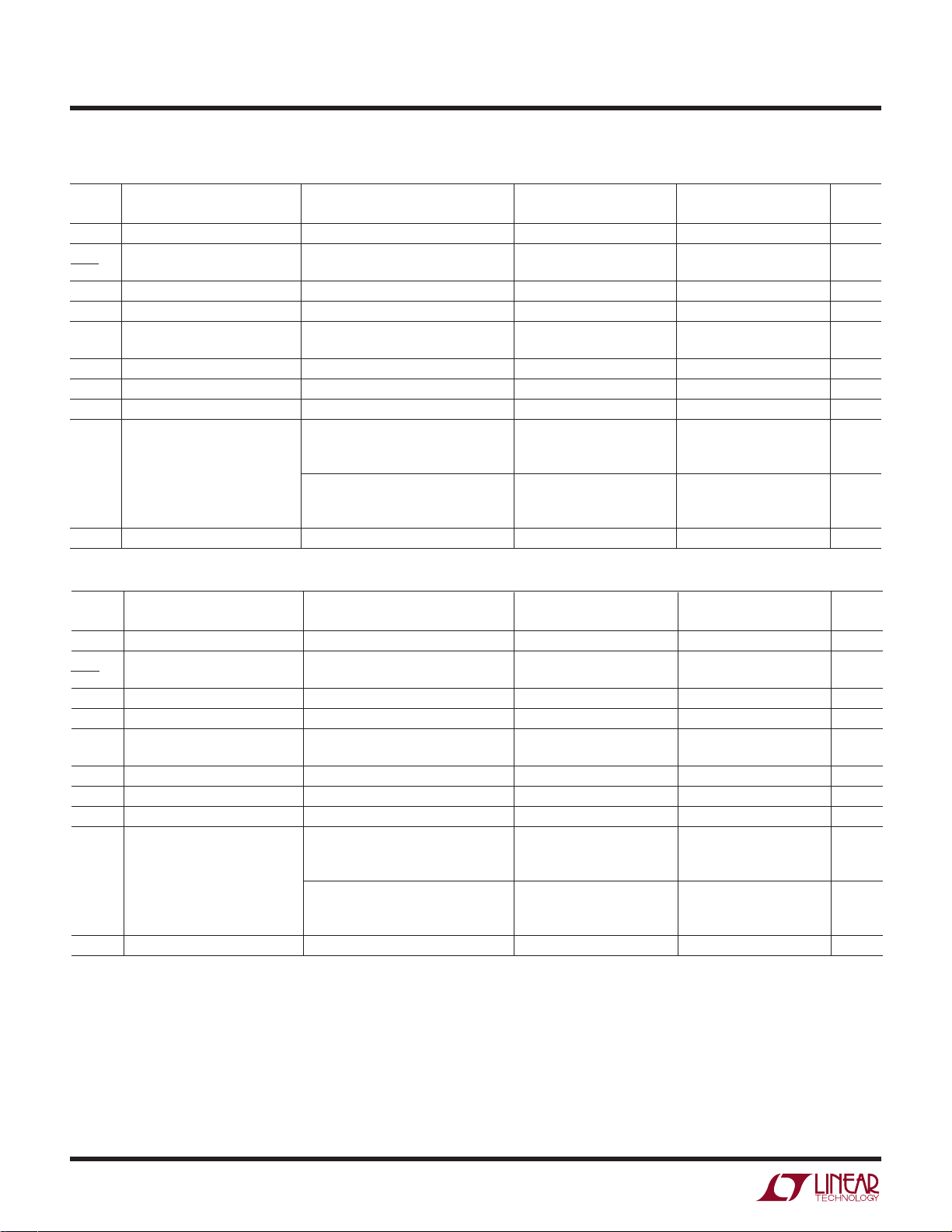
LT1215/LT1216
LECTRICAL C CHARA TERIST
E
5V
VS = 5V, VCM = 0.5V, V
SYMBOL PARAMETER CONDITIONS MIN TYP MAX MIN TYP MAX UNITS
V
OS
∆V
∆T
I
OS
I
B
CMRR Common Mode Rejection Ratio VCM = 0.1V to 2.9V 89 108 85 108 dB
PSRR Power Supply Rejection Ratio VS = 2.6V to 12.5V 95 114 92 114 dB
A
VOL
I
S
Input Offset Voltage 200 350 250 550 µV
Input Offset Voltage Drift 8-Pin DIP Package 1 2.5 2 5 µV/°C
OS
(Note 6) 14-Pin DIP, SO Package 3 10 µV/°C
Input Offset Current 35 100 35 170 nA
Input Bias Current 450 530 450 830 nA
Input Voltage Range 2.9 3.1 2.9 3.1 V
Large-Signal Voltage Gain VO = 0.05V to 3.7V, RL = 500Ω 100 600 100 600 V/mV
Maximum Output Voltage Swing Output High, No Load 4.20 4.33 4.20 4.33 V
(Note 7) Output High, I
Supply Current Per Amplifier 3.3 5.2 7.5 3.3 5.2 7.5 mA
= 0.5V, 0°C ≤ TA ≤ 70°C, unless otherwise noted.
OUT
Output High, I
Output Low, No Load 0.006 0.009 0.006 0.009 V
Output Low, I
Output Low, I
ICS
LT1215AC LT1215C/LT1216C
0.1 –0.1 0.1 –0.1 V
= 1mA 4.10 4.24 4.10 4.24 V
SOURCE
= 20mA 3.70 3.89 3.70 3.89 V
SOURCE
= 1mA 0.035 0.055 0.035 0.055 V
SINK
= 20mA 0.500 0.725 0.500 0.725 V
SINK
VS = 5V, VCM = 0.5V, V
SYMBOL PARAMETER CONDITIONS MIN TYP MAX MIN TYP MAX UNITS
V
OS
∆V
∆T
I
OS
I
B
CMRR Common Mode Rejection Ratio VCM = 0.2V to 2.8V 88 108 84 108 dB
PSRR Power Supply Rejection Ratio VS = 2.7V to 12.5V 94 114 91 114 dB
A
VOL
I
S
Input Offset Voltage 200 400 250 600 µV
Input Offset Voltage Drift 8-Pin DIP Package 1 2.5 2 5 µV/°C
OS
(Note 6) 14-Pin DIP, SO Package 3 10 µV/°C
Input Offset Current 35 110 35 190 nA
Input Bias Current 450 550 450 850 nA
Input Voltage Range 2.8 3.0 2.8 3.0 V
Large-Signal Voltage Gain VO = 0.05V to 3.7V, RL = 500Ω 100 600 100 600 V/mV
Maximum Output Voltage Swing Output High, No Load 4.10 4.30 4.10 4.30 V
(Note 7) Output High, I
Supply Current Per Amplifier 2.9 5.3 7.6 2.9 5.3 7.6 mA
= 0.5V, –40°C ≤ TA ≤ 85°C, unless otherwise noted. (Note 4)
OUT
0.2 0 0.2 0 V
= 1mA 4.00 4.16 4.00 4.16 V
Output High, I
Output Low, No Load 0.006 0.010 0.006 0.010 V
Output Low, I
Output Low, I
SOURCE
= 20mA 3.60 3.82 3.60 3.82 V
SOURCE
= 1mA 0.035 0.060 0.035 0.060 V
SINK
= 20mA 0.500 0.750 0.500 0.750 V
SINK
LT1215AC LT1215C/LT1216C
4
LT1215/LT1216
LECTRICAL C CHARA TERIST
E
5V
VS = 5V, VCM = 0.5V, V
SYMBOL PARAMETER CONDITIONS MIN TYP MAX MIN TYP MAX UNITS
V
OS
∆V
∆T
I
OS
I
B
CMRR Common Mode Rejection Ratio VCM = 0.4V to 2.8V 87 108 82 108 dB
PSRR Power Supply Rejection Ratio VS = 2.7V to 12.5V 93 114 90 114 dB
A
VOL
I
S
Input Offset Voltage 250 450 350 750 µV
Input Offset Voltage Drift 1 2.5 2 5 µV/°C
OS
(Note 6)
Input Offset Current 35 150 35 200 nA
Input Bias Current 450 600 450 700 nA
Input Voltage Range 2.8 3.0 2.8 3.0 V
Large-Signal Voltage Gain VO = 0.05V to 3.7V, RL = 500Ω 50 100 50 100 V/mV
Maximum Output Voltage Swing Output High, No Load 4.00 4.20 4.00 4.20 V
(Note 7) Output High, I
Supply Current Per Amplifier 2.3 5.5 8.4 2.3 5.5 8.4 mA
= 0.5V, –55°C ≤ TA ≤ 125°C, unless otherwise noted.
OUT
Output High, I
Output Low, No Load 0.007 0.012 0.007 0.012 mV
Output Low, I
Output Low, I
ICS
LT1215AM LT1215M
0.4 0.2 0.4 0.2 V
= 1mA 3.90 4.10 3.90 4.10 V
SOURCE
= 20mA 3.50 3.80 3.50 3.80 V
SOURCE
= 1mA 0.040 0.070 0.040 0.070 mV
SINK
= 20mA 0.700 1.000 0.700 1.000 mV
SINK
+
15V
–
VS = ±15V, VCM = 0V, V
SYMBOL PARAMETER CONDITIONS MIN TYP MAX MIN TYP MAX UNITS
V
OS
I
OS
I
B
CMRR Common Mode Rejection Ratio VCM = –15V to 13V 90 108 86 108 dB
PSRR Power Supply Rejection Ratio VS = ±2V to ±18V 96 110 93 110 dB
A
VOL
I
O
SR Slew Rate AV = –2 (Note 8) 40 50 40 50 V/µs
GBW Gain-Bandwidth Product f = 100kHz 15 23 15 23 MHz
I
S
LECTRICAL C CHARA TERIST
E
= 0V, TA = 25°C, unless otherwise noted.
OUT
Input Offset Voltage 225 500 250 650 µV
Input Offset Current 30 80 30 110 nA
Input Bias Current 360 500 360 550 nA
Input Voltage Range 13.0 13.2 13.0 13.2 V
Large-Signal Voltage Gain VO = 0V to ±10V, RL = 2k 1000 3500 1000 3500 V/mV
Maximum Output Voltage Swing Output High, I
Output Low, I
Maximum Output Current (Note 11) ±30 ±50 ±30 ±50 mA
Supply Current Per Amplifier 3.6 5.7 8 3.6 5.7 8 mA
Channel Separation VO = ±10V, RL = 2k 128 140 128 140 dB
Minimum Supply Voltage Equal Split Supplies ±1.7 ±2 ±1.7 ±2V
Full-Power Bandwidth AV = 1, VO = 20V
Settling Time 0.01%, AV = 1, ∆VO = 10V 480 480 ns
SOURCE
SINK
P-P
ICS
LT1215AC LT1215C/LT1215M
LT1215AM LT1216C
–15.0 –15.2 –15.0 – 15.2 V
= 30mA 13.5 13.75 13.5 13.75 V
= 30mA –14 –14.4 –14 –14.4 V
750 750 kHz
5
LT1215/LT1216
+
15V
–
VS = ±15V, VCM = 0V, V
SYMBOL PARAMETER CONDITIONS MIN TYP MAX MIN TYP MAX UNITS
V
OS
∆V
OS
∆T
I
OS
I
B
CMRR Common Mode Rejection Ratio VCM = –14.9V to 12.9V 89 108 85 108 dB
PSRR Power Supply Rejection Ratio VS = ±2.1V to ±18V 95 110 92 110 dB
A
VOL
I
S
LECTRICAL C CHARA TERIST
E
= 0V, 0°C ≤ TA ≤ 70°C, unless otherwise noted.
OUT
Input Offset Voltage 325 550 400 750 µV
Input Offset Voltage Drift 8-Pin DIP Package 1 2.5 2 5 µV/°C
(Note 6) 14-Pin DIP, SO Package 3 10 µV/°C
Input Offset Current 30 100 30 160 nA
Input Bias Current 360 530 360 800 nA
Input Voltage Range 12.9 13.1 12.9 13.1 V
Large-Signal Voltage Gain VO = 0V to ±10V, RL = 2k 800 3000 800 3000 V/mV
Maximum Output Voltage Swing Output High, I
Output Low, I
Supply Current Per Amplifier 3.3 6.3 9.2 3.3 6.3 9.2 mA
SOURCE
SINK
ICS
LT1215AC LT1215C/LT1216C
–14.9 –15.1 –14.9 –15.1 V
= 20mA 13.7 13.9 13.7 13.9 V
= 20mA –14.2 –14.5 –14.2 –14.5 V
VS = ±15V, VCM = 0V, V
SYMBOL PARAMETER CONDITIONS MIN TYP MAX MIN TYP MAX UNITS
V
OS
∆V
∆T
I
OS
I
B
CMRR Common Mode Rejection Ratio VCM = –14.8V to 12.8V 88 108 84 108 dB
PSRR Power Supply Rejection Ratio VS = ±2.2V to ±18V 94 110 91 110 dB
A
VOL
I
S
Input Offset Voltage 325 600 400 800 µV
Input Offset Voltage Drift 8-Pin DIP Package 1 2.5 2 5 µV/°C
OS
(Note 6) 14-Pin DIP, SO Package 3 10 µV/°C
Input Offset Current 30 110 30 180 nA
Input Bias Current 360 550 360 820 nA
Input Voltage Range 12.8 13.0 12.8 13.0 V
Large-Signal Voltage Gain VO = 0V to ±10V, RL = 2k 800 2500 800 2500 V/mV
Maximum Output Voltage Swing Output High, I
Supply Current Per Amplifier 2.9 6.5 9.5 2.9 6.5 9.5 mA
VS = ±15V, VCM = 0V, V
SYMBOL PARAMETER CONDITIONS MIN TYP MAX MIN TYP MAX UNITS
V
OS
∆V
∆T
I
OS
I
B
CMRR Common Mode Rejection Ratio VCM = –14.6V to 12.8V 87 108 82 108 dB
PSRR Power Supply Rejection Ratio VS = ±2.2V to ±15V 93 110 90 110 dB
A
VOL
I
S
Input Offset Voltage 350 650 500 950 µV
Input Offset Voltage Drift 1 2.5 2 5 µV/°C
OS
(Note 6)
Input Offset Current 30 150 30 200 nA
Input Bias Current 360 600 360 700 nA
Input Voltage Range 12.8 13.0 12.8 13.0 V
Large-Signal Voltage Gain VO = 0V to ±10V, RL = 2k 500 2000 500 2000 V/mV
Maximum Output Voltage Swing Output High, I
Supply Current Per Amplifier 2.3 7 10.3 2.3 7 10.3 mA
= 0V, –40°C ≤ TA ≤ 85°C, unless otherwise noted. (Note 4)
OUT
–14.8 –15.0 –14.8 –15.0 V
= 20mA 13.6 13.8 13.6 13.8 V
SOURCE
Output Low, I
= 0V, –55°C ≤ TA ≤ 125°C, unless otherwise noted.
OUT
Output Low, I
= 20mA –14.1 –14.5 –14.1 –14.5 V
SINK
–14.6 –14.8 –14.6 –14.8 V
= 20mA 13.4 13.8 13.4 13.8 V
SOURCE
= 20mA –14 –14.5 –14 –14.5 V
SINK
LT1215AC LT1215C/LT1216C
LT1215AM LT1215M
6
 Loading...