

FEATURES
■
Voltage Noise: 1.2nV/√Hz Max at 1kHz
0.9nV/√Hz Typ at 1kHz
■
Voltage and Current Noise 100% Tested
■
Gain-Bandwidth Product: 40MHz Min
■
Slew Rate: 10V/µs Min
■
Voltage Gain: 2 Million Min
■
Low THD at 10kHz, AV = –10, RL = 600Ω: 0.002%
VO = 7V
■
Low IMD, CCIF Method, AV = +10: 0.002%
RMS
RL = 600Ω
VO = 7V
RMS
U
APPLICATIO S
LT1115
Ultralow Noise,
Low Distortion, Audio Op Amp
U
DESCRIPTIO
The LT®1115 is the lowest noise audio operational amplifier available. This ultralow noise performance (0.9nV/√Hz
at 1kHz) is combined with high slew rates (>15V/µs) and
very low distortion specifications.
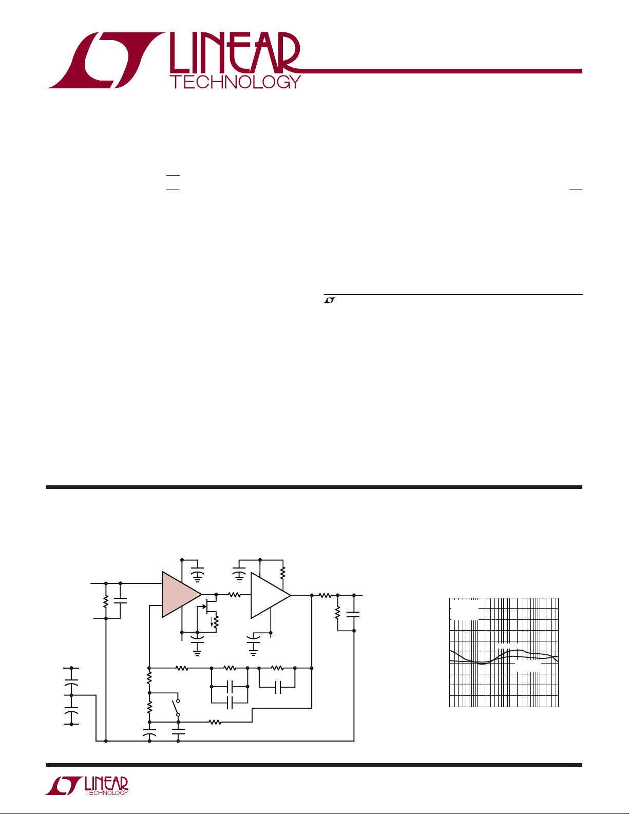
The RIAA circuit shown below using the LT1115 has very
low distortion and little deviation from ideal RIAA
response (see graph).
, LTC and LT are registered trademarks of Linear Technology Corporation.
■
High Quality Audio Preamplifiers
■
Low Noise Microphone Preamplifiers
■
Very Low Noise Instrumentation Amplifiers
■
Low Noise Frequency Synthesizers
■
Infrared Detector Amplifiers
■
Hydrophone Amplifiers
■
Low Distortion Oscillators
U
TYPICAL APPLICATIO
RIAA Phonograph Preamplifier (40/60db Gain)
18V 18V
COM
+
V
–
V
INPUT
47.5k (MM)
R
IN
100Ω (MC)
COM
18V
+
470µF
35V
+
470µF
35V
–18V
SINGLE
POINT
BOARD
GROUND
C
IN
(SELECT
PER
PHOTO
CARTRIDGE)
22.6Ω
210Ω
+
2200µF
16V
+ +
3
7
+
A1
LT1115
2
–
4
–18V
499Ω
OPEN—MM
CLOSED—MC
4.7µF
FILM
1µF
1µF
35V
35V
100Ω
6
2N4304*
~250Ω
SELECT
2mA
FOR 2mA
1µF
1µF
35V
35V
17.8k
330pF
3900pF
82.5k
BYPASS SUPPLIES WITH LOW ESR CAPS
NOTE:
OTHER CAPS: HIGH QUALITY FILM
R
BOOST
49.9Ω
2
1
4
A2
LT1010CT
+ +
RESISTORS 1%
*OR USE 2mA CURRENT SOURCE
MM = MOVING MAGNET
MC = MOVING COIL
5
3
–18V
210k
15nF
562Ω
25k
R
L
LT1115 • TA01
OUTPUT
3900pF
Measured Deviation from RIAA
Response. lnput at 1kHz = 1mV
Pre-Emphasized
1.0000
VS= ± 18V
0.80000
0.60000
0.40000
0.20000
–0.2000
DEVIATION (dB)
–0.4000
–0.6000
–0.8000
–1.000
=25Ω
R
S
=25°C
T
A
100
FREQUENCY (Hz)
MEASURED
COMPUTER
SIMULATED
1k 10k 50k
0.0
20
RMS
LT1115 • TA02
1115fa
1
LT1115
WWWU
ABSOLUTE AXI U RATI GS
(Note 1)
Supply Voltage ...................................................... ±22V
Differential Input Current (Note 5) ...................... ±25mA
Input Voltage ............................ Equal to Supply Voltage
Output Short-Circuit Duration .......................... Indefinite
U
PACKAGE DESCRIPTIO
Operating Temperature Range ..................... 0°C to 70°C
Storage Temperature Range ..................–65°C to 150°C
Lead Temperature (Soldering, 10 sec).................. 300°C
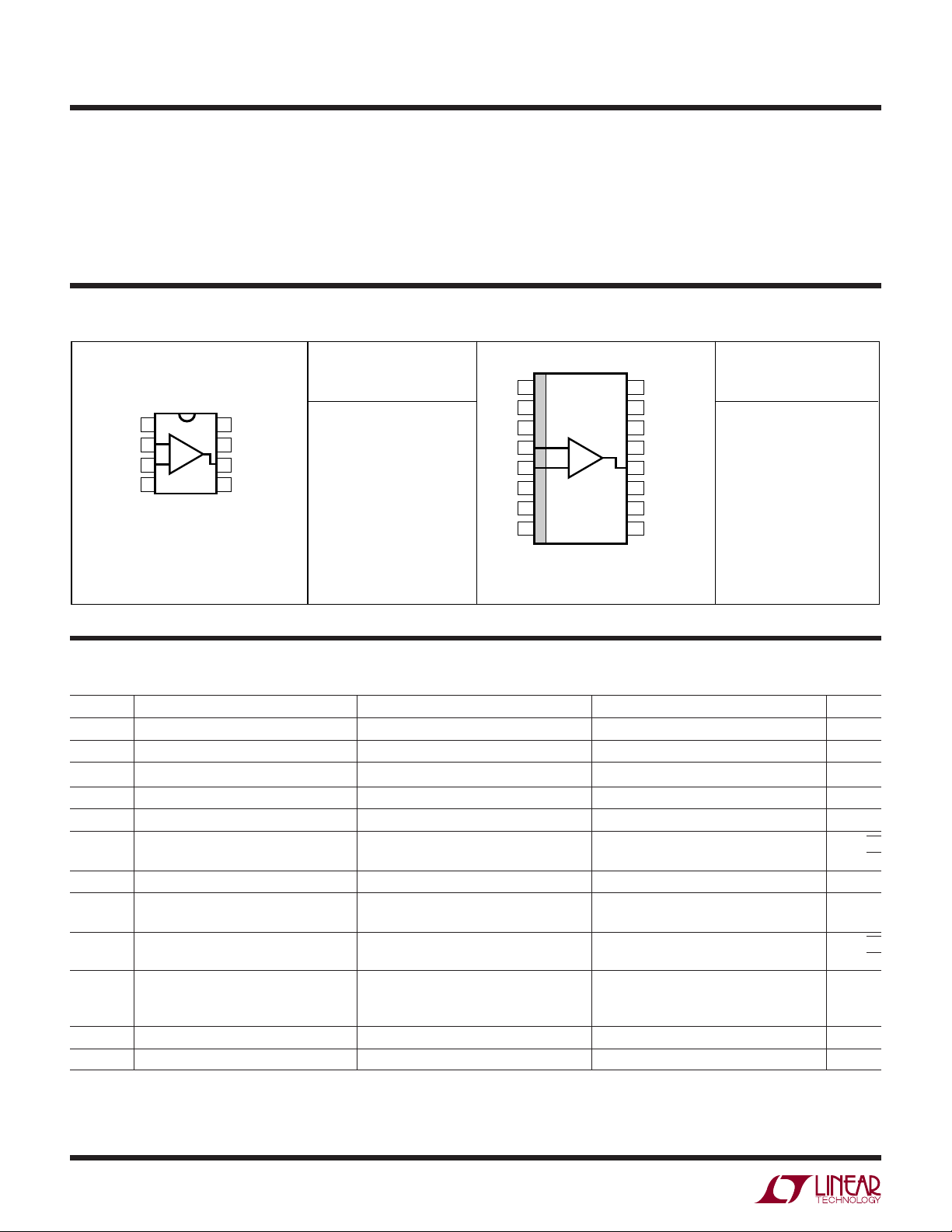
TOP VIEW
1
2
3
4
5
6
7
8
T
MAX
–
+
SW PACKAGE
16-LEAD PLASTIC SO
= 115°C, θJA = 130°C/W
16
15
14
13
12
11
10
9
NC
NC
TRIM
+
V
OUTPUT
OVERCOMP
NC
NC
ORDER
PART NUMBER
LT1115CSW
LT1115 • POI01
TOP VIEW
V
OS
1
TRIM
–IN
+IN
T
JMAX
–
2
+
3
–
4
V
N PACKAGE
8-LEAD PDIP
= 115°C, θJA = 130°C/W
8
7
6
5
V
OS
TRIM
+
V
OUT
OVERCOMP
ORDER
PART NUMBER
LT1115CN8
TRIM
–IN
+IN
NC
NC
NC
NC
–
V
Consult LTC Marketing for parts specified with wider operating temperature ranges.
ELECTRICAL CHARACTERISTICS
VS = ±18V, TA = 25°C, unless otherwise noted.
SYMBOL PARAMETER CONDITIONS MIN TYP MAX UNITS
THD Total Harmonic Distortion at 10kHz Av = –10, VO = 7V
IMD Inter-Modulation Distortion (CCIF) Av = 10, VO = 7V
V
OS
I
OS
I
B
e
n
Input Offset Voltage (Note 2) 50 200 µV
Input Offset Current VCM = 0V 30 200 nA
Input Bias Current VCM = 0V ±50 ±380 nA
Input Noise Voltage Density fo = 10Hz 1.0 nV/√Hz
, RL = 600 < 0.002 %
RMS
, RL = 600 < 0.0002 %
RMS
fo = 1000Hz, 100% tested 0.9 1.2 nV/√Hz
Wideband Noise DC to 20kHz 120 nV
RMS
Corresponding Voltage Level –136 dB
re 0.775V
i
n
Input Noise Current Density fo = 10Hz 4.7 pA/√Hz
(Note 3) fo = 1000Hz, 100% tested 1.2 2.2 pA/√Hz
Input Resistance
Common Mode 250 MΩ
Differential Mode 15 kΩ
Input Capacitance 5pF
Input Voltage Range ±13.5 ±15.0 V
2
1115fa
LT1115
ELECTRICAL CHARACTERISTICS
SYMBOL PARAMETER CONDITIONS MIN TYP MAX UNITS
CMRR Common Mode Rejection VCM = ±13.5V 104 123 dB
Ratio
PSRR Power Supply Rejection VS = ±4V to ±19V 104 126 dB
Ratio
A
VOL
V
OUT
SR Slew Rate A
GBW Gain-Bandwidth Product fo = 20kHz (Note 4) 40 70 MHz
Z
o
I
S
The
● denotes specifications which apply over the full operating temperature range, otherwise specifications are at T
Large-Signal Voltage Gain RL ≥ 2kΩ, Vo = ±14.5V 2.0 20 V/µV
Maximum Output Voltage No Load ±15.5 ±16.5 V
Swing R
Open Loop 0utput Impedance Vo = 0, Io = 0 70 Ω
Supply Current 8.5 11.5 mA
VS = ±18V, TA = 25°C, unless otherwise noted.
≥ 1kΩ, Vo = ±13V 1.5 15 V/µV
R
L
≥ 600Ω, Vo = ±10V 1.0 10 V/µV
R
L
≥ 2kΩ ±14.5 ±15.5 V
L
≥ 600Ω ±11.0 ±14.5 V
R
L
= –1 10 15 V/µs
VCL
= 25°C.
A
VS = ±18V, unless otherwise noted.
SYMBOL PARAMETER CONDITIONS MIN TYP MAX UNITS
V
OS
∆VOS/∆TAverage Input Offset Drift 0.5 µV/°C
I
OS
I
B
CMRR Common Mode Rejection V
PSRR Power Supply Rejection VS = ±4.5V to ±18V ● 100 123 dB
A
VOL
V
OUT
I
S
Input Offset Voltage (Note 2) ● 75 280 µV
Input Offset Current VCM = 0V ● 40 300 nA
Input Bias Current VCM = 0V ● ±70 ±550 nA
Input Voltage Range ● ±13 ±14.8 V
= ±13V ● 100 120 dB
Ratio
Ratio
Large-Signal Voltage Gain RL ≥ 2kΩ, Vo = ±13V ● 1.5 15 V/µV
Maximum Output Voltage No Load ±15 ±16.3 V
Swing R
Supply Current ● 9.3 13 mA
CM
RL ≥ 1kΩ, Vo = ±11V 1.0 10 V/µV
≥ 2kΩ ● ±13.8 ±15.3 V
L
R
≥ 600Ω ±10 ±14.3 V
L
Note 1: Absolute Maximum Ratings are those values beyond which the life
of a device may be impaired.
Note 2: Input Offset Voltage measurements are performed by automatic
test equipment approximately 0.5 sec after application of power.
Note 3: Current noise is defined and measured with balanced source
resistors. The resultant voltage noise (after subtracting the resistor noise
on an RMS basis) is divided by the sum of the two source resistors to
obtain current noise.
Note 4: Gain-bandwidth product is not tested. It is guaranteed by design
and by inference from the slew rate measurement.
Note 5: The inputs are protected by back-to-back diodes. Current limiting
resistors are not used in order to achieve low noise. If differential input
voltage exceeds ±1.8V, the input current should be limited to 25mA.
1115fa
3
LT1115
FREQUENCY (Hz)
20
0.001
0.010
0.1
100
1k
20k
TOTAL HARMONIC DISTORTION + NOISE (%)
A
V
= 1000
V
IN
= 20mV
P-P
(7mV
RMS)
V
OUT
= 20V
P-P
(7V
RMS)
T
A
= 25°C
R
L
= 600
V
S
= ±18V
LT1115 • TPC09
UW
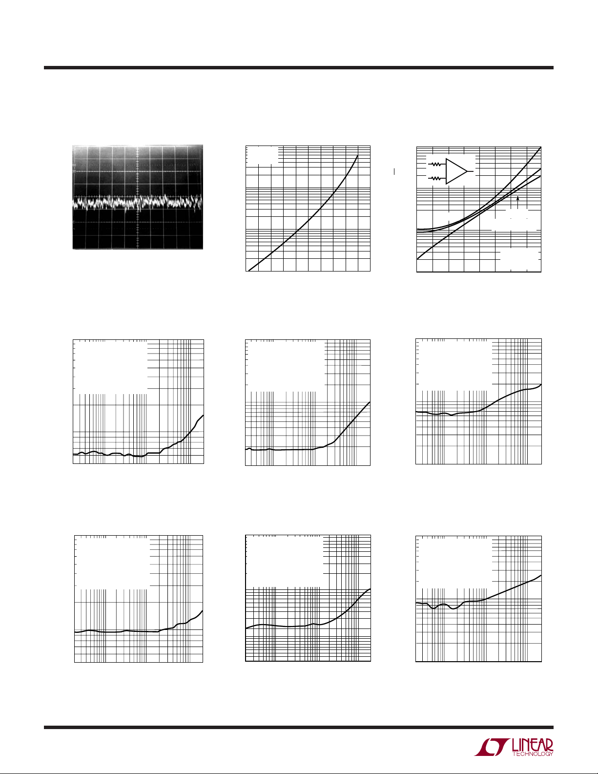
TYPICAL PERFOR A CE CHARACTERISTICS
Wideband Noise, DC to 20kHz
0.5µV/DIV
FPO
0.5ms/DIV
THD + Noise vs Frequency
(A
= –10)
V
A
R
V
V
T
V
= –10
V
= 600
L
= 2V
IN
OUT
= 25°C
A
= ±18V
S
= 20V
P-P
(700mV
(7V
P-P
RMS)
RMS)
0.010
Wideband Voltage Noise
(0.1Hz to Frequency Indicated)
10
VS = ± 18V
= 25°C
T
A
1
0.1
RMS VOLTAGE NOISE (µV)
0.01
100
1k
BANDWIDTH (Hz)
10k
100k
THD + Noise vs Frequency
(A
= –100)
V
0.1
A
= –100
V
= 600
R
L
V
0.010
IN
V
OUT
T
A
V
S
= 200mV
= 25°C
= ±18V
= 20V
P-P
P-P
(70mV
(7V
RMS)
RMS)
1M
LT1115 • TPC02
10M
Total Noise vs Matched Source
Resistance
100
R
S
–
R
S
+
10
AT 10Hz
1.0
TOTAL NOISE DENSITY (nV/√Hz)
0.1
3
1
MATCHED SOURCE RESISTANCE, RS (Ω)
30
10
100
300
2 RS NOISE ONLY
THD + Noise vs Frequency
(A
= –1000)
V
0.1
AV = – 1000
= 600
R
L
V
= 20mV
= 20V
P-P
P-P
(7mV
(7V
RMS)
RMS)
0.010
V
T
A
V
IN
OUT
= 25°C
= ±18V
S
AT 1kHz
VS= ± 18V
=25°C
T
A
1k 3k
10k
LT1115 • TPC03
0.001
TOTAL HARMONIC DISTORTION + NOISE (%)
0.0005
20
100 1k
FREQUENCY (Hz)
THD + Noise vs Frequency
(A
= 10)
V
20
A
V
R
V
IN
V
OUT
T
A
V
S
= 10
= 600
L
= 2V
(700mV
P-P
= 20V
P-P
= 25°C
= ±18V
100 1k
(7V
RMS)
FREQUENCY (Hz)
0.010
0.001
TOTAL HARMONIC DISTORTION + NOISE (%)
0.0005
RMS)
LT1115 • TPC04
LT1115 • TPC07
TOTAL HARMONIC DISTORTION + NOISE (%)
0.001
20k
20
100 1k
THD + Noise vs Frequency
(A
= 100)
V
0.1
A
= 100
V
V
= 200mV
IN
V
= 20mV
OUT
T
= 25°C
A
= 600
R
L
= ±18V
V
S
0.010
0.001
TOTAL HARMONIC DISTORTION + NOISE (%)
0.0005
20
20k
100 1k
FREQUENCY (Hz)
(700V
P-P
RMS)
(7V
P-P
RMS)
FREQUENCY (Hz)
20k
LT1115 • TPC05
20k
LT1115 • TPC08
TOTAL HARMONIC DISTORTION + NOISE (%)
0.001
20
100 1k
FREQUENCY (Hz)
THD + Noise vs Frequency
(A
= 1000)
V
20k
LT1115 • TPC06
4
1115fa
TEMPERATURE (°C)
0
0
RMS VOLTAGE NOISE DENSITY (nV/√Hz)
0.8
1.2
30
2.0
0.4
15 75
60
45
1.6
V
S
= ±18V
AT 10Hz
AT 1kHz
LT1115 • TPC15
UW
TYPICAL PERFOR A CE CHARACTERISTICS
LT1115
CCIF IMD Test (Twin Equal
Amplitude Tones at 13 and 14kHz)*
0.1
A
= 10
V
= 600
R
L
= 25°C
T
A
= ±18V
V
S
0.010
0.001
INTERMODULATION DISTORTION (at 1kHz) (%)
0.0001
10m
0.1
OUTPUT AMPLITUDE (V
1
RMS
)
LT1115 • TPC10
10
CCIF IMD Test (Twin Equal
Amplitude Tones at 13 and 14kHz)*
0.1
A
= 10
V
= 10k
R
L
T
= 25°C
A
= ±18V
V
S
0.010
0.001
INTERMODULATION DISTORTION (at 1kHz) (%)
0.0001
10m
0.1
OUTPUT AMPLITUDE (V
Total Noise vs Unmatched Source
Resistance Current Noise Spectrum
100
R
S
10
100
10
Slew Rate, Gain-Bandwidth-Product
vs Overcompensation Capacitor
100
10
SLEW
1
SLEW RATE (V/µs)
C
FROM PIN 5 TO PIN 6
OC
= ±18V
V
S
= 25°C
T
A
0.1
1 100
1
RMS
10
)
LT1115 • TPC11
10
OVERCOMPENSATION CAPACITOR (pF)
1000
GWB
LT1115 • TPC12
10000
10000
GAIN AT 20kHz
1000
100
10
Voltage Noise vs Temperature
AT 10Hz
1.0
TOTAL NOISE DENSITY (nV/√Hz)
0.1
1
3
UNMATCHED SOURCE RESISTANCE, RS (Ω)
30
10
100
AT 1kHz
RS NOISE ONLY
V
= ± 18V
S
T
= 25°C
A
1k 3k
300
10k
LT1115 • TPC13
CURRENT NOISE DENSITY (pA/√Hz)
0.1
1
10
TYPICAL
1/f CORNER = 250Hz
100
FREQUENCY (Hz)
Voltage Noise vs Supply Voltage Supply Current vs Temperature
RMS VOLTAGE NOISE DENSITY (nV/√Hz)
1.25
0.75
1.5
1.0
0.5
T
0
= 25°C
A
AT 1kHz
± 5
± 10
SUPPLY VOLTAGE (V)
± 15
±20
LT1115 • TPC16
10
9
8
7
6
5
4
3
SUPPLY CURRENT (mA)
2
1
0
0
V
S
V
S
V
15
TEMPERATURE (°C)
= ±18V
= ±15V
= ±5V
S
30
45
1k
10k
LT1115 • TPC14
Output Short-Circuit Current
vs Time
60
LT1115 • TPC17
50
40
30
20
10
0
–10
–20
–30
SHORT-CIRCUIT CURRENT (mA)
SINKING SOURCING
–40
75
–50
01
TIME FROM OUTPUT SHORT TO GROUND (MINUTES)
VS = ± 18V
25°C
25°C
23
LT1115 • TPC18
*See CCIF Test Note at end of “Typical Performance Characteristics”.
1115fa
5

LT1115
COMMON MODE LIMIT (V)
REFERRED TO POWER SUPPLY
–1
–2
–3
–4
+4
+3
+2
+1
V
+
V
S
= ± 18V
V
S
= ± 5V
V
S
= ± 5V TO ±18V
TEMPERATURE (°C)
0
30
15
75
60
45
V
–
LT1115 • TPC24
UW
TYPICAL PERFOR A CE CHARACTERISTICS
Voltage Gain vs Frequency
160
140
120
100
80
60
40
VOLTAGE GAIN (dB)
20
VS = ± 18V
T
= 25°C
0
A
= 2k
R
L
–20
0.01
0.1
10 100
1
FREQUENCY (Hz)
1k
10k
100k 1M 10M
Voltage Gain vs Load Resistance
100
VS = ±18V
T
= 25°C
A
= 27mA AT 25°C
I
LMAX
10
VOLTAGE GAIN (V/µV)
1
0.1
LOAD RESISTANCE (kΩ)
1
100M
LT1115 • TPC19
LT1115 • TPC22
VOLTAGE GAIN (dB)
–10
OVERSHOOT (% )
10
Gain, Phase vs Frequency
70
60
50
40
30
20
10
0
VS = ±18V
T
A
C
L
10k
= 25°C
= 10pF
100k 1M
PHASE
GAIN
FREQUENCY (Hz)
Capacitance Load Handling
80
70
60
50
40
30
20
10
0
10
30pF
R
S
+
–
A
= –1, R
V
A
= – 10
V
= 200Ω
R
S
A
= – 100
V
= 20Ω
R
S
CAPACITIVE LOAD,
2k
C
L
= 2k
S
100 1000
10M
CL (pF)
LT1115 • TPC20
VS = ±18V
T
= 25°C
A
LT1115 • TPC23
70
60
PHASE MARGIN (DEGREES)
50
40
30
20
10
0
–10
100M
10000
Voltage Gain vs Supply Voltage
100
T
= 25°C
A
RL = 2kΩ
RL = 600Ω
10
VOLTAGE GAIN (V/µV)
1
0 ± 20
± 5
± 10
SUPPLY VOLTAGE (V)
± 15
Common Mode Limit Over
Temperature
LT1115 • TPC21
Common Mode Rejection Ratio
vs Frequency
140
120
100
80
60
40
20
COMMON MODE REJECTION RATIO (dB)
VS = ± 18V
T
A
0
10 100
6
= 25°C
1k
FREQUENCY (Hz)
10k
100k
1M
LT1115 • TPC25
10M
Power Supply Rejection Ratio
vs Frequency
160
140
120
100
80
60
40
POWER SUPPLY REJECTION RATIO (dB)
20
VS = ±18V
T
= 25°C
A
0
POSITIVE
SUPPLY
FREQUENCY (Hz)
NEGATIVE
SUPPLY
10k 100k 1M 10M0.1 1 10 100 1k
LT1115 • TPC26
Large-Signal Transient Response
5V/DIVISION
FPO
AV = –1
R
= Rf = 2k
S
= 30pF
C
f
1µs/DIVISION
1115fa

UW
TYPICAL PERFOR A CE CHARACTERISTICS
Maximum Output vs Frequency
Small-Signal Transient Response
(Power Bandwidth*)
30
25
V
= ±18V
S
T
A
R
L
= 25°C
= 2kΩ
LT1115
Closed-Loop Output Impedance
100
IO = 1mA
= ±18V
V
S
T
= 25°C
A
10
20
20mV/DIVISION
AV = –1,
= Rf = 2kΩ
R
S
= 30pF
C
f
C
= 80pF
L
FPO
0.2µs/DIVISION
15
10
PEAK-TO-PEAK OUTPUT VOLTAGE (V)
5
0
10k
CCIF Testing
Note: The CCIF twin-tone intermodulation test inputs two closely
spaced equal amplitude tones to the device under test (DUT). The
FPO
analyzer then measures the intermodulation distortion (IMD)
produced in the DUT by measuring the difference tone equal to the
spacing between the tones.
The amplitude of the lMD test input is in sinewave peak equivalent
terms. As an example, selecting an amplitude of 1.000V will result in
the complex IMD signal having the same 2.828V peak-to-peak
amplitude that a 1.000V sinewave has. Clipping in a DUT will thus
occur at the same input amplitude for THD + N and IMD modes.
WUUU
APPLICATIO S I FOR ATIO
*POWER BANDWIDTH
SLEW RATE
fP
=
πE
OP
fP
= POWER BANDWIDTH
E
=
PEAK-TO-PEAK AMPLIFIER
P-P
OUTPUT VOLTAGE
100k
FREQUENCY (Hz)
1M 10M
LT1115 • TPC29
0.1
OUTPUT IMPEDANCE (Ω)
0.01
0.001
1
A
= 1000
V
A
= 5
V
100
10
10k
1k
FREQUENCY (Hz)
100k
1M
LT1115 • TPC30
The LT1115 is a very high performance op amp, but
not necessarily one which is optimized for universal
application. Because of very low voltage noise and the
resulting high gain-bandwidth product, the device is most
applicable to relatively high gain applications. Thus, while
the LT1115 will provide notably superior performance to
the 5534 in most applications, the device may require
circuit modifications to be used at very low noise gains.
The part is not generally applicable for unity gain followers
or inverters. In general, it should always be used with good
low impedance bypass capacitors on the supplies, low
impedance feedback values, and minimal capacitive loading. Ground plane construction is recommended, as is a
compact layout.
Voltage Noise vs Current Noise
The LT1115’s less than 1nV/√Hz voltage noise matches
that of the LT1028 and is three times better than the lowest
voltage noise heretofore available (on the LT1007/1037).
A necessary condition for such low voltage noise is
operating the input transistors at nearly 1mA of
collector currents, because voltage noise is inversely
proportional to the square root of the collector current.
Current noise, however, is directly proportional to the
square root of the collector current. Consequently, the
LT1115’s current noise is significantly higher than on
most monolithic op amps.
1115fa
7

LT1115
WUUU
APPLICATIO S I FOR ATIO
Therefore, to realize truly low noise performance it is
important to understand the interaction between voltage
noise (en), current noise (in) and resistor noise (rn).
Total Noise vs Source Resistance
The total input referred noise of an op amp is given by
et = [e
2
+ r
n
+ (inReq)2]
n
1/2
2
where Req is the total equivalent source resistance at
the two inputs
and rn = √4kTR
= 0.13√R
eq
in nV/√Hz at 25°C
eq
As a numerical example, consider the total noise at 1kHz
of the gain of 1000 amplifier shown below.
100Ω
100Ω
R
= 100Ω + 100Ω||100k ≈ 200Ω
eq
100k
–
LT1115
+
LT1115 • AI01
rn = 0.13√200 = 1.84nV/√Hz
The plot also shows that current noise is more dominant
at low frequencies, such as 10Hz. This is because resistor
noise is flat with frequency, while the 1/f corner of current
noise is typically at 250Hz. At 10Hz when R
> 1kΩ, the
eq
current noise term will exceed the resistor noise.
When the source resistance is unmatched, the Total Noise
vs Unmatched Source Resistance plot should be consulted. Note that total noise is lower at source resistances
below 1kΩ because the resistor noise contribution is less.
When Rs > 1kΩ total noise is not improved, however. This
is because bias current cancellation is used to reduce
input bias current. The cancellation circuitry injects two
correlated current noise components into the two inputs.
With matched source resistors the injected current noise
creates a common-mode voltage noise and gets rejected
by the amplifier. With source resistance in one input only,
the cancellation noise is added to the amplifier’s inherent
noise.
In summary, the LT1115 is the optimum amplifier for
noise performance—provided that the source resistance
is kept low. The following table depicts which op amp
manufactured by Linear Technology should be used to
minimize noise—as the source resistance is increased
beyond the LT1115’s level of usefulness.
en = 0.85nV/√Hz
in = 1.0pA/√Hz
et = [0.852 + 1.842 + (1.0 x 2.0)2]
1/2
= 2.04nV/√Hz
output noise = 1000 et = 2.04µV/√Hz
At very low source resistance (Req < 40Ω) voltage noise
dominates. As Req is increased resistor noise becomes the
largest term—as in the example above—and the LT1115’s
voltage noise becomes negligible. As Req is further
increased, current noise becomes important. At 1kHz,
when Req is in excess of 20kΩ, the current noise
component is larger than the resistor noise. The Total
Noise vs Matched Source Resistance plot in the Typical
Performance Characteristics section, illustrates the above
calculations.
Best Op Amp for Lowest Total Noise vs Source Resistance
SOURCE RESISTANCE BEST OP AMP
(NOTE 1) AT LOW FREQ (10Hz) WIDEBAND (1kHz)
0 to 400Ω LT1028/1115 LT1028/1115
400Ω to 4kΩ LT1007/1037 LT1028/1115
4kΩ to 40kΩ LT1001* LT1007/1037
40kΩ to 500kΩ LT1012* LT1001*
500kΩ to 5MΩ LT1012* or LT1055 LT1012*
> 5M LT1055 LT1055
Note 1: Source resistance is defined as matched or unmatched, e.g.,
= 1kΩ means: 1kΩ at each input, or 1kΩ at one input and zero at the
R
S
other.
*These op amps are best utilized in applications requiring less bandwidth
than audio.
1115fa
8

TYPICAL APPLICATIO S
LT1115
U
INPUT
R1
1k, 0.1%
R
30k
1%
R2
1k, 0.1%
18V
+
2
7
3
–
LT1115
+
4
–18V
P
316k, 0.1%
1µF 35V
LOW ESR
6
1µF 35V
+
LOW ESR
R4
316k, 0.1%
R3
4.7µF
FILM
10k
1%
NOTE: MATCH RESISTOR PAIRS
R1
R2
Figure 1. Balanced Transformerless Microphone Preamp
THD + Noise vs Frequency
(Figure 1)
1
T
= 25°C
A
= 100kΩ
R
L
V
= 10mV
IN
OUT
= 150Ω
S
= 2.92V
RMS
RMS
V
R
100
1%
=
R3
R4
OUT
TO ± 0.1%
LT1115 • TA03
0.1
TOTAL HARMONIC DISTORTION + NOISE (%)
0.010
20
100
1k
FREQUENCY (Hz)
20k
LT1115 • TA04
1115fa
9

LT1115
TYPICAL APPLICATIO S
U
18V
+
1µF
35V
3
INPUT
R1
100Ω
2
–18V
1µF
35V
OPTIONAL SERVO LOOP
LOWERS OFFSET TO < 50µV
NOTE 1: USE SINGLE POINT GROUND.
NOTE 2: USE ≥ 470µF CAPACITORS AT EACH
INCOMING SUPPLY TERMINAL (I.E. AT BOARD EDGE).
+
LT1115
–
33.2k
1%
7
~250Ω
SELECT
FOR 2mA
1µF
100Ω
2N4304*
2mA
6
C1
8
1
4
33pF
+
33.2k
1%
18V
49.9Ω
R
BOOST
LT1010CT
IN
R2
909Ω
–18V
18V
+
1µF
35V
6
LT1097
–18V
NOTE 3: FOR BETTER NOISE PERFORMANCE AT
SLIGHTLY LESS DRIVE CAPABILITY: R1 = 43Ω,
R2 = 392Ω DELETE C1.
+
1µF
35V
+
V
OUTPUT
–
V
RESISTORS 1% METAL FILM
CAPACITORS – BYPASS; LOWER ESR
OTHER: POLYESTER OR OTHER
HIGH QUALITY FILM.
1µF
*OR USE 2mA CURRENT SOURCE.
35V
+
100k
7
2
–
3
+
4
100k
1µF
+
35V
R
L
1µF
LT1115 • TA05
10
Figure 2. Low Noise DC Accurate x 10 Buffered Line Amplifier
THD + Noise vs Frequency
(Figure 2)
0.010
T
= 25°C
A
= ± 18V
V
S
V
= 500mV
IN
= 10Ω
= 600Ω
= 5V
RMS
100
RMS
1k
FREQUENCY (Hz)
20k
LT1115 • TA07
V
OUT
R
S
R
L
0.001
TOTAL HARMONIC DISTORTION + NOISE (%)
0.0001
20
1115fa

TYPICAL APPLICATIO S
GAIN: 40dB
30dB
INPUT
100µF
+
35V
18V
–18V
18V
–18V
100µF
RESISTORS 1% METAL FILM
+
35V
CAPACITORS—BYPASS: LOW ESR
OTHER: HIGH QUALITY FILM
NOTE 1: USE SINGLE POINT
GROUNDING TECHNIQUES
U
0.01µF
24.9Ω
75Ω
100Ω
2
3
–
+
100k
100pF
2.49k
LT1115
LT1115
475Ω
OUTPUT
TO
18V
+
7
6
4
6
LT1097
1µF
100V
– 18V
1µF
35V
7
3
+
2
–
4
1µF
+
35V
1M
1M
LT1115 • TA06
RIAA
STAGE
1µF
100V
Figure 3. RIAA Moving Coil “Pre-Pre” Amplifier
(40/30dB Gain Low Noise Servo’d Amplifier)
CCIF IMD Test (Twin Tones at 13
and 14kHz) (Figure 3)
0.1
TA = 25°C
= ± 18V
V
S
= 100k
R
L
0.010
0.001
0.0001
0.1
INTERMODULATION DISTORTION (AT 1kHz) (IMD) (%)
OUTPUT AMPLITUDE (
1
V
)
RMS
LT1115 • TA08
Noise vs Frequency (Figure 3)
10µ
T
= 25°C
A
= ±18V
V
S
INPUT GROUNDED
1µ
NOISE (V)
100n
10
10n
100 1k
20
NOTE: NOISE AT 1kHz REFERRED TO INPUT ~2nV
FREQUENCY (Hz)
20k
LT1115 • TA09
1115fa
11

LT1115
TYPICAL APPLICATIO S
U
18V
MOVING COIL
INPUT
100Ω
12.1Ω
1µF
35V
+
2
–
3
+
0.01µF
LT1115
4
7
100pF
2.49k
+
6
1µF
35V
RIAA NETWORK
R1
6081Ω
C1
0.1645µF
–18V
+
+
470µF
35V
470µF
35V
C2
0.483µF
R2
490Ω
3
2
499Ω
+
LT1056
–
Figure 4. Moving Coil Passive RIAA Phonograph Pre-Amp
+
1µF
35V
7
6
4
10k
1µF
+
35V
NOTE 1: 1kHz GAIN = 53dB
NOTE 2: IN RIAA NETWORK VALUES SHOWN
ARE MEASURED AND PRODUCE THE
“DEVIATION FROM RIAA” GRAPH SHOWN.
THE CALCULATED EXACT VALUES ARE:
R1-6249Ω C1-0.161µF
R2-504Ω C2-0.47µF
4.7µFFILM
499Ω
100k
RESISTORS 1% METAL FILM
CAPACITORS—BYPASS: LOW ESR
OTHER: HIGH QUALITY FILM
OUTPUT
LT1115 • TA10
Deviation from RIAA Response
Input at 1kHz = 232µV
Pre-Emphasized (Figure 4)
0.50000
0.40000
0.30000
0.20000
0.10000
0.0
–0.1000
DEVIATION (dB)
–0.2000
–0.3000
–0.4000
–0.5000
20
VS = ±18V
= 100k
R
L
= 10Ω
R
S
= 25°C
T
A
100
RMS
1k
FREQUENCY (Hz)
20k
LT1115 • TA11
THD + Noise vs Frequency
Input at 1kHz = 232µV
RMS
Pre-Emphasized (Figure 4)
0.1
V
= ±18V
S
= 100k
R
L
= 10Ω
R
S
= 25°C
T
A
0.010
TOTAL HARMONIC DISTORTION + NOISE (%)
0.001
20
100
FREQUENCY (Hz)
1k
20k
LT1115 • TA12
12
1115fa

TYPICAL APPLICATIO S
2.5k
REV. AUDIO
TAPER
U
1µF
35V
18V
+
470µF
35V
+
1N4002
49.9Ω
LT1115
+
1µF
35V
150Ω
MICROPHONE
INPUT
RED
BRN
CASE
JENSEN
JE-16-A/B
BLK
WHT
YELLOW
6.19k
ORANGE
6
22Ω
2N4304**
–18V
1µF
35V
1µF
35V
100pF
100Ω
~250Ω
SELECT
FOR 2mA
1N4002
+
6
+
18V
LT1097
4
–18V
IN
470µF
35V
7
+
V
LT1010CT
–
2
+
3
–
V
+ +
100k
1µF
35V
BOOST
OUT
100k
2.49k
RESISTORS 1% METAL FILM
CAPACITORS—BYPASS: LOW ESR
OTHER: HIGH QUALITY FILM
NOTE: USE SINGLE POINT GROUND
JENSEN NETWORK VALUES—FACTORY SELECTED.
*
JE-16-A/B & JE-11-BM AVAILABLE FROM:
JENSEN TRANSFORMERS
10735 BURBANK BLVD.
N. HOLLYWOOD, CA 91601
(213) 876-0059
**
OR USE 2mA CURRENT SOURCE
1µF
10Ω
4.99Ω
100Ω
10k
2
3
–
+
LT1115
7
4
2mA
1µF
35V
+
1µF
Figure 5. High Performance Transformer Coupled Microphone Pre-Amp
10Ω
OPTIONAL
SINGLE-ENDED TO
BALANCED OUTPUT
TRANSFORMER
BRN
RED
JENSEN
JE-11-BM
YEL
LT1115 • TA13
Risetime of High Performance
Transformer Coupled Microphone
Pre-Amp (Figure 5)
RISETIME OF PRE-AMP
A
= 20dB
V
= 400mV
V
IN
2kHz SQUARE WAVE MEASURED AT SINGLEENDED OUTPUT BEFORE TRANSFORMER
THD + Noise vs Frequency
(Gain = 20dB) Balanced In/
Balanced Out (Figure 5)
1
V
= ±18V
S
= 0.95V
V
IN
= 600Ω
L
= 150Ω
S
= 25°C
A
RMS
FREQUENCY (Hz)
R
R
T
0.1
0.010
0.001
TOTAL HARMONIC DISTORTION + NOISE (%)
0.0005
20 100 1k 20k
LT1115 • TA15
Frequency Response
(Gain = 20dB) Balanced In/
Balanced Out (Figure 5)
1.0000
0.0
– 1.000
– 2.000
– 3.000
V
= ±18V
S
= 0.95V
V
IN
= 600Ω
L
= 150Ω
S
= 25°C
A
RMS
100
FREQUENCY (Hz)
1k
AMPLITUDE (dB) REFERRED TO 1kHz
– 5.000
R
T
10
R
– 4.000
10k
100k
LT1115 • TA16
1115fa
13

LT1115
TYPICAL APPLICATIO S
U
15V
–15V
2k
3
2
5.6k
10pF
10µF
+
+
LT1115
–
120k
1µF
+
1µF
35V
4
R1
15V
7
4
–15V
1k
7
LT1006
+
+
15V
–
+
200Ω
1µF
35V
1µF
35V
10k 10k
C2
0.1µF
FILM
1µF
35V
100Ω
15V
R
= 49.9Ω
BOOST
+
2
–15V
4
3
4.7k
2.5V
LT1004's
1.2V
INTO 100Ω
P-P
1µF
+
35V
5
IN
LT1010
1
MOUNT,
1N4148's
IN CLOSE
PROXIMITY
<5ppm DISTORTION AND NOISE
AT 1kHz, 20V
MEASUREMENT LIMITED BY RESOLUTION
OF AUDIO PRECISION TEST SYSTEM
ALL BYPASS CAPACITORS: LOW ESR
FILM CAPACITORS = ASC TYPE 315
OUTPUT
20V
P-P
–15V
1
f =
2πRC
WHERE R1C1 = R2C2
MEASURED WITH
R1 = R2 = 1.5k
LT1115 • TA17
C1
0.1µF FILM
200Ω
15V
+
1µF
35V
6
LT1022
4
+
470µF
1µF
35V
35V
+
–15V
470µF
+
35V
VACTEC
VTL 5C10
R2
7
–
2
+
3
2k
500Ω
(20T)
2.4k
+
100Ω
14
Figure 6. Ultralow THD Oscillator (Sine Wave) (< 5ppm Distortion)
1115fa

PACKAGE DESCRIPTIO
U
N8 Package
8-Lead PDIP (Narrow .300 Inch)
(Reference LTC DWG # 05-08-1510)
.255 ± .015*
(6.477 ± 0.381)
.400*
(10.160)
MAX
87 6
LT1115
5
12
.300 – .325
(7.620 – 8.255)
.065
(1.651)
.008 – .015
(0.203 – 0.381)
+.035
.325
–.015
+0.889
8.255
()
–0.381
NOTE:
1. DIMENSIONS ARE
*THESE DIMENSIONS DO NOT INCLUDE MOLD FLASH OR PROTRUSIONS.
MOLD FLASH OR PROTRUSIONS SHALL NOT EXCEED .010 INCH (0.254mm)
INCHES
MILLIMETERS
TYP
.045 – .065
(1.143 – 1.651)
.100
(2.54)
BSC
3
4
.130 ± .005
(3.302 ± 0.127)
.120
(3.048)
MIN
.018 ± .003
(0.457 ± 0.076)
.020
(0.508)
MIN
N8 1002
Information furnished by Linear Technology Corporation is believed to be accurate and reliable.
However, no responsibility is assumed for its use. Linear Technology Corporation makes no representation that the interconnection of its circuits as described herein will not infringe on existing patent rights.
1115fa
15

LT1115
PACKAGE DESCRIPTIO
.030 ±.005
TYP
N
U
SW Package
16-Lead Plastic Small Outline (Wide .300 Inch)
(Reference LTC DWG # 05-08-1620)
.050 BSC
.045 ±.005
16
N
.398 – .413
(10.109 – 10.490)
15 14
NOTE 4
13
12
10 9
11
.420
MIN
123 N/2
RECOMMENDED SOLDER PAD LAYOUT
.291 – .299
(7.391 – 7.595)
NOTE 4
.010 – .029
.005
(0.127)
RAD MIN
.009 – .013
(0.229 – 0.330)
NOTE:
1. DIMENSIONS IN
2. DRAWING NOT TO SCALE
3. PIN 1 IDENT, NOTCH ON TOP AND CAVITIES ON THE BOTTOM OF PACKAGES ARE THE MANUFACTURING OPTIONS.
THE PART MAY BE SUPPLIED WITH OR WITHOUT ANY OF THE OPTIONS
4. THESE DIMENSIONS DO NOT INCLUDE MOLD FLASH OR PROTRUSIONS.
MOLD FLASH OR PROTRUSIONS SHALL NOT EXCEED .006" (0.15mm)
(0.254 – 0.737)
NOTE 3
INCHES
(MILLIMETERS)
× 45°
.016 – .050
(0.406 – 1.270)
.325 ±.005
0° – 8° TYP
NOTE 3
.093 – .104
(2.362 – 2.642)
(1.270)
1
.050
BSC
.014 – .019
(0.356 – 0.482)
2345
TYP
6
N/2
78
(0.940 – 1.143)
.394 – .419
(10.007 – 10.643)
.037 – .045
.004 – .012
(0.102 – 0.305)
S16 (WIDE) 0502
16
Linear Technology Corporation
1630 McCarthy Blvd., Milpitas, CA 95035-7417
(408) 432-1900 ● FAX: (408) 434-0507
●
www.linear.com
1115fa
LW/TP 1102 1K REV A • PRINTED IN USA
LINEAR TECHNOLOGY CORPORATION 1989
 Loading...