

Datasheet LT1081IN, LT1081CSW, LT1081CN, LT1081CJ, LT1081 Datasheet (Linear Technology)
...
FEATURES
LT1080/LT1081
Advanced Low Power
5V RS232 Dual Driver/Receiver
U
DESCRIPTIO
■
Superior to CMOS
– Improved Speed: Operates over 120kBaud
– Improved Protection: Outputs Can Be Forced
to ±30V without Damage
– Three-State Outputs Are High
Impedance When Off
– Only Needs 1µF Capacitors
■
Absolutely No Latchup
■
CMOS Comparable Low Power: 60mW
■
Can Power Additional RS232 Drivers: 10mA
■
Supply Current in Shutdown: 1µA
■
Available in SO Package
■
Available with or without Shutdown
U
APPLICATIO S
■
Portable Computers
■
Battery-Powered RS232 Systems
■
Power Supply Generator
■
Terminals
■
Modems
The LT®1080/LT1081 are the only dual RS232 driver/
receiver with charge pump to guarantee absolutely no
latchup. These interface optimized devices provide a realistic balance between CMOS levels of power dissipation
and real world requirements for ruggedness. The driver
outputs are fully protected against overload and can be
shorted to ±30V. Unlike CMOS, the advanced architecture
of the LT1080/LT1081 does not load the signal line when
“shut down” or when power is off. Both the receiver and
RS232 outputs are put into a high impedance state. An
advanced output stage allows driving higher capacitive
loads at higher speeds with exceptional ruggedness
against ESD.
For applications requiring up to five drivers and five
receivers with charge pump in one package see the LT1130A
Series data sheet. A version of the LT1080/LT1081, the
LT1180A and LT1181A that use only 0.1µF capacitors, is
also available. All of Linear Technology’s RS232 ICs are
available in standard surface mount packages.
, LTC and LT are registered trademarks of Linear Technology Corporation.
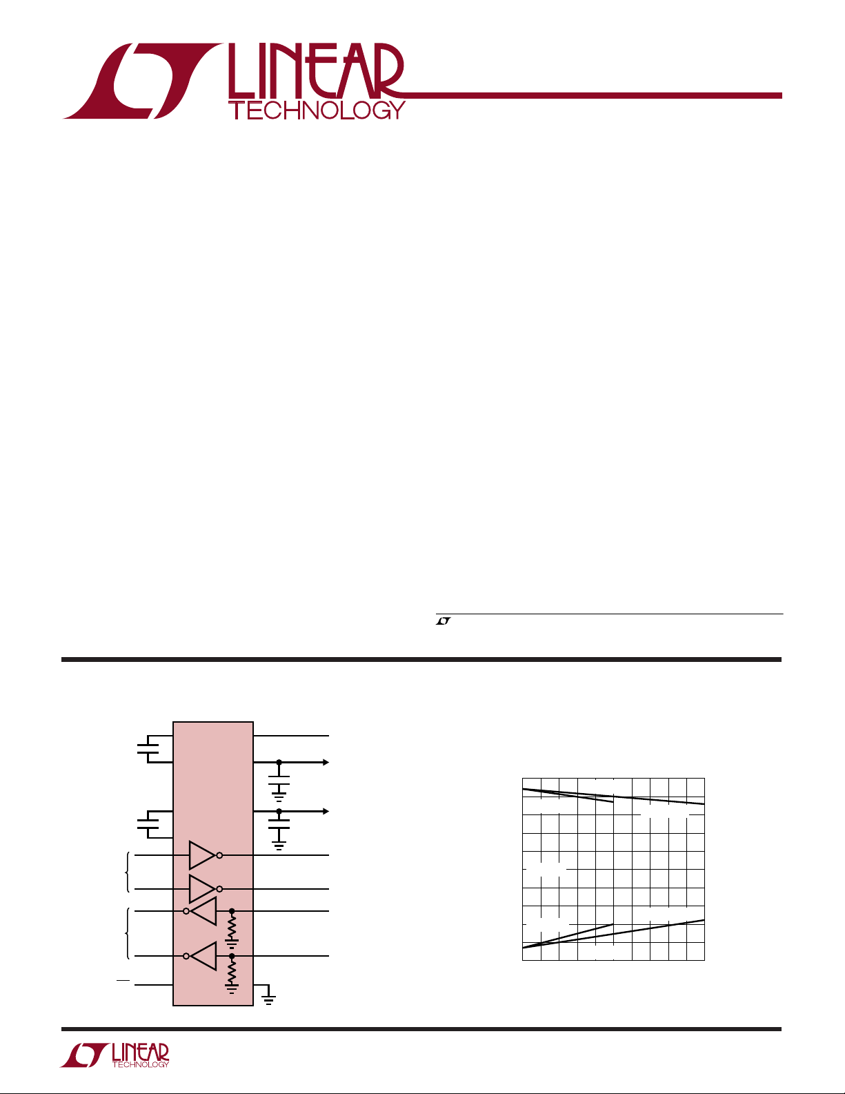
TYPICAL APPLICATIO
LOGIC
INPUTS
LOGIC
OUTPUTS
ON/OFF
1µF
1µF
2
4
LT1080
5
6
12
11
13
10
18
17
3
7
15
8
14
5k
9
5k
16
U
1µF
1µF
5V INPUT
9V OUTPUT
–9V OUTPUT
RS232 OUTPUT
RS232 OUTPUT
RS232 INPUT
RS232 INPUT
1080/81 • TA01
Supply Generator Outputs
10
8
RL TO V
6
4
2
VCC = 5V
0
–2
–4
OUTPUT VOLTAGE (V)
–6
RL TO V
–8
–10
02468101214161820
V+ OUTPUT
–
+
V– OUTPUT
OUTPUT CURRENT (mA)
RL TO GND
RL TO GND
1080/81 TA01a
1
LT1080/LT1081
A
W
O
LUTEXI TIS
S
A
WUW
U
ARB
G
Supply Voltage (VCC) ................................................. 6V
+
V
...........................................................................................
–
V
.......................................................................................
12V
–12V
Input Voltage
Driver ........................................................... V– to V
Receiver ................................................. –30V to 30V
ON/OFF Pin .............................................. GND to 12V
Output Voltage
Driver ................................. (V– + 30V) to (V+ – 30V)
Receiver .................................. –0.3V to (VCC + 0.3V)
WU
/
TOP VIEW
1
2
3
4
5
6
7
8
9
SW PACKAGE
O
RDER I FOR ATIO
ORDER PART
ON/OFF
18
V
17
CC
GND
16
TR1 OUT
LT1080
15
REC1 IN
14
REC1 OUT
13
TR1 IN
12
TR2 IN
11
REC2 OUT
10
N PACKAGE
18-LEAD PDIP
NUMBER
LT1080CJ
LT1080CN
LT1080CSW
LT1080IN
LT1080ISW
LT1080MJ
PACKAGE
NC
+
C1
+
V
–
C1
+
C2
–
C2
–
V
TR2 OUT
REC2 IN
J PACKAGE
18-LEAD CERDIP
18-LEAD PLASTIC SO WIDE
T
= 150°C, θJA = 100°C/W, θJC = 40°C/W (J)
JMAX
T
= 150°C, θJA = 120°C/W, θJC = 50°C/W (N)
JMAX
= 150°C, θJA = 90°C/W, θJC = 26°C/W (SW)
T
JMAX
(Note 1)
Short-Circuit Duration
+
V
......................................................................................
–
V
......................................................................................
Driver Output ............................................... Indefinite
+
Receiver Output ........................................... Indefinite
Operating Temperature Range
LT1080C/LT1081C ................................. 0°C to 70°C
LT1080I/LT1081I................................ –40°C to 85°C
LT1080M/LT1081M.......................... –55°C to 125°C
Storage Temperature Range ..................–65°C to 150°C
Lead Temperature (Soldering, 10 sec)................. 300°C
U
TOP VIEW
+
1
C1
+
2
V
–
3
C1
+
C2
–
C2
–
V
TR2 OUT
REC2 IN
J PACKAGE
16-LEAD CERDIP
T
= 150°C, θJA = 100°C/W, θJC = 40°C/W (J)
JMAX
T
= 150°C, θJA = 120°C/W, θJC = 50°C/W (N)
JMAX
= 150°C, θJA = 95°C/W, θJC = 27°C/W (SW)
T
JMAX
LT1081
4
5
6
7
8
SW PACKAGE
16-LEAD PLASTIC SO WIDE
16
15
14
13
12
11
10
9
N PACKAGE
16-LEAD PDIP
V
CC
GND
TR1 OUT
REC1 IN
REC1 OUT
TR1 IN
TR2 IN
REC2 OUT
ORDER PART
NUMBER
LT1081CJ
LT1081CN
LT1081CSW
LT1081IN
LT1081ISW
LT1081MJ
30 sec
30 sec
2
LT1080/LT1081
LECTRICAL C CHARA TERIST
E
ICS
temperature range, otherwise specifications are at T
The ● denotes the specifications which apply over the full operating
= 25°C. (Note 2)
A
PARAMETER CONDITIONS MIN TYP MAX UNITS
Driver
Output Voltage Swing Load = 3k to GND Both Outputs Positive ● 5 7.3 V
● –5 –6.5 V
Logic Input Voltage Level Input Low Level (V
Input High Level (V
Logic Input Current V
≥ 2V ● 520 µA
IN
V
≤ 0.8V ● 520 µA
IN
Output Short-Circuit Current Sourcing Current, V
Sinking Current, V
= High) ● 1.4 0.8 V
OUT
= Low) ● 2 1.4 V
OUT
OUT
= 0V –9 –12 mA
OUT
Output Leakage Current SHUTDOWN (Note 3), V
Negative
= 0V 9 12 mA
= ±30V ● 10 100 µA
OUT
Data Rate (Note 6) RL = 3k, CL = 2500pF 120 kBd
= 3k, CL = 1000pF 250 kBd
R
L
Slew Rate RL = 3k, C
= 51pF 4 15 30 V/µs
L
Receiver
Input Voltage Thresholds Input Low Threshold Commercial ● 0.8 1.3 V
Industrial and Military
● 0.2 1.3 V
Input High Threshold Commercial ● 1.7 2.4 V
Industrial and Military
● 1.7 3.0 V
Hysteresis ● 0.1 0.4 1 V
Input Resistance V
Output Voltage Output Low, I
Output Short-Circuit Current Sinking Current, V
Output Leakage Current SHUTDOWN (Note 3), 0V ≤ V
= ±10V 3 5 7 kΩ
IN
= –1.6mA ● 0.2 0.4 V
Output High, I
Sourcing Current, V
OUT
= 160µA (VCC = 5V) ● 3.5 4.8 V
OUT
= V
OUT
CC
= 0V 0.6 1 mA
OUT
≤ V
OUT
CC
–10 –20 mA
● 110 µA
Power Supply Generator (Note 4)
V+ Output Voltage I
V– Output Voltage I
= 0mA 8.0 9.0 V
OUT
= 10mA 7.0 8.0 V
I
OUT
= 15mA 6.5 7.5 V
I
OUT
= 0mA –7.5 –8.5 V
OUT
I
= –10mA –5.5 –6.5 V
OUT
= –15mA –5.0 –6.0 V
I
OUT
Supply Current ● 12 22 mA
Supply Leakage Current (V
ON/OFF Pin Current 0V ≤ V
) SHUTDOWN (Note 3), LT1080 Only ● 1 100 µA
CC
≤ 5V, LT1080 Only ● –15 80 µA
ON/OFF
Supply Rise Time (Note 5), LT1080 Only 1 ms
Note 1: Absolute Maximum Ratings are those values beyond which the life
of a device may be impaired.
Note 2: These parameters apply for 4.5V ≤ V
≤ 5.5V and V
CC
ON/OFF
= 3V,
unless otherwise specified.
Note 3: V
50°C ≤ T
= 0.4V for –55°C ≤ TA ≤ 50°C, and V
ON/OFF
≤ 125°C. (LT1080 only)
A
ON/OFF
= 0.2V for
Note 4: Unless otherwise specified, V
–
V
equals zero and the driver outputs are low (inputs high).
Note 5: Time from either SHUTDOWN high or power on until V
–
V
≤ –6V. All external capacitors are 1µF.
= 5V, external loading of V+ and
CC
+
≥ 6V and
Note 6: Data rate operation guaranteed by slew rate, short-circuit current
and propagation delay tests.
3
LT1080/LT1081
UUU
PI FU CTIO S
(Pin numbers refer to LT1080)
C1+; C1–; C2+; C2– (Pins 2, 4, 5, 6): Requires an external
capacitor (≥1µF) from C1
+
to C1– and another from C2
+
to C2–. Pin 2 can be used for connecting a second positive
supply. When a separate positive supply is used, C1 can be
deleted.
V+ (Pin 3): Positive Supply for RS232 Drivers.
+
V
≈ 2VCC – 1.5V. Requires an exterenal capacitor (≥1µF)
for charge storage. May be loaded (up to 15mA) for
external system use. Loading does reduce V+ voltage (see
graphs). Capacitor may be tied to ground or +5V input
supply. With multiple transceivers, the V+ and V– pins may
be paralleled into common capacitors.
V– (Pin 7): Negative Supply for RS232 Drivers.
–
V
≈ –(2V
– 2.5V). Requires an external capacitor
CC
(≥1µF) for charge stroage. May be loaded (up to –15mA)
for external system use. Loading does reduce V– voltage
(see graphs). With multiple transceivers, the V+ and V
–
pins may be paralleled into common capacitors.
TR2 OUT; TR1 OUT (Pins 8, 15): Driver Outputs with
RS232 Voltage Levels. Outputs are in a high impedance
state when in the SHUTDOWN mode or when power is off
(VCC = 0V) to allow data line sharing. Outputs are fully
short-circuit protected from (V– + 30V) to (V+ – 30V) with
power on, off or in the SHUTDOWN mode. Typical output
breakdowns are greater than ±45V and higher applied
voltages will not damage the device if moderately current
limited. Shorting one output will affect output from the
other.
REC2 IN; REC1 IN (Pins 9, 14): Receiver Inputs. Accepts
RS232 voltage levels (±30V) and has 0.4V of hysteresis to
provide noise immunity. Input impedance is nominally
5kΩ.
REC2 OUT; REC1 OUT (Pins 10, 13): Receiver Outputs
with TTL/CMOS Voltage Levels. Outputs are in a high
impedance state when in the SHUTDOWN mode to allow
data line sharing. Outputs are fully short-circuit protected
to ground or VCC with power on, off or in the SHUTDOWN
mode.
TR2 IN; TR1 IN (Pins 11, 12): RS232 Driver Input Pins.
Inputs are TTL/CMOS compatible. Inputs should not be
allowed to float. Tie unused inputs to VCC.
GND (Pin 16): Ground Pin.
VCC (Pin 17): Input Supply Pin. Supply current drops to
zero in the SHUTDOWN mode.
ON/OFF (Pin 18): Contols the operation mode of the
LT1080 and is TTL/CMOS compatible. A logic low puts the
device in the SHUTDOWN mode which reduces input
supply current to zero and places both driver and receiver
outputs in a high impedance state. A logic high fully
enables the device.
UW
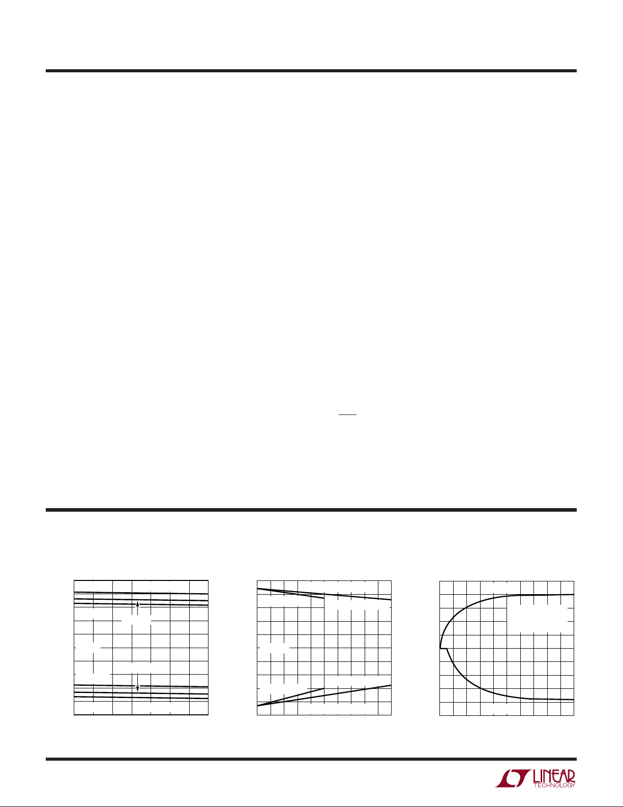
TYPICAL PERFOR A CE CHARACTERISTICS
Driver Output Voltage Supply Generator Outputs
10
VCC = 5.5V
8
6
VCC = 4.5V
4
2
RL = 3k
0
–2
–4
VCC = 4.5V
–6
DRIVER OUTPUT VOLTAGE (V)
–8
VCC = 5.5V
–10
–55 –25 0 25 50 75 100 125
OUTPUT HIGH
VCC = 5V
VCC = 5V
OUTPUT LOW
TEMPERATURE (°C)
1080/81 G01
10
8
LOADED TO V
6
4
2
VCC = 5V
0
–2
–4
OUTPUT VOLTAGE (V)
–6
LOADED TO V
–8
–10
02468101214161820
V+ OUTPUT VOLTAGE
–
LOADED TO GROUND
LOADED TO GROUND
+
V– OUTPUT VOLTAGE
OUTPUT CURRENT (mA)
4
1080/81 G02
Supply Generation from V
or Shutdown
10
8
6
4
2
0
–2
–4
SUPPLY VOLTAGE (V)
–6
–8
–10
0 0.2 0.4 0.6 0.8 1.0 1.2 1.4 1.6 1.8 2.0
V+ SUPPLY
V– SUPPLY
TIME (ms)
VCC = 5V
C1 TO C4 = 1µF
= 4.7k; V+ TO V
R
L
CC
–
1080/81 G03

UW
TEMPERATURE (°C)
OUTPUT LEAKAGE CURRENT (µA)
100
10
1
0.1
1080/81 G09
V
OUT
= –30V
V
OUT
= 30V
–55 –25 0 25 50 75 100 125
TYPICAL PERFOR A CE CHARACTERISTICS
Receiver Output
Receiver Input Thresholds
3.00
2.75
2.50
2.25
2.00
1.75
1.50
1.25
INPUT THRESHOLD (V)
1.00
0.75
0.50
–55 –25 0 25 50 75 100 125
INPUT HIGH
INPUT LOW
TEMPERATURE (°C)
1080/81 G04
ON/OFF Pin Thresholds Supply Current in Shutdown
5.0
4.5
4.0
3.5
3.0
2.5
2.0
1.5
ON/OFF PIN VOLTAGE (V)
1.0
0.5
MAXIMUM OFF VOLTAGE
0
–55 –25 0 25 50 75 100 125
MINIMUM ON VOLTAGE
TEMPERATURE (°C)
1080/81 G07
Short-Circuit Current ON/OFF Pin Current vs Voltage
100
OUTPUT SINKING
10
1
OUTPUT CURRENT (mA)
0.1
–55 –25 0 25 50 75 100 125
1000
100
10
SUPPLY CURRENT (nA)
1
–55 –25 0 25 50 75 100 125
OUTPUT SOURCING
TEMPERATURE (°C)
VCC = 5V
TEMPERATURE (°C)
1080/81 G05
1080/81 G08
LT1080/LT1081
40
35
30
25
20
15
10
5
INPUT CURRENT (µA)
0
–5
–10
012345
Driver Output Leakage in
Shutdown
INPUT VOLTAGE (V)
1080/81 G06
Output Waveforms
5V
DRIVER
0V
OUTPUT
–5V
RECEIVER
OUTPUT5V0V
5V
INPUT
0V
02µs4µs6µs8µs 0 1ms 2ms 3ms 4ms 0 1ms 2ms 3ms 4ms
V
= 5V 1080/81 G10.tiff
CC
RL = 3k
DRIVER
OUTPUT
HIGH
RECEIVER
OUTPUT
LOW
ON/OFF
INPUT
Shutdown to Driver Output
10V
5V
0V
0V
–5V
–10
5V
0V
RL = 3k
RECEIVER
OUTPUT
ON/OFF
INPUT5V0V
Shutdown to Receiver Output
6V
4V
2V
0V
V
= 5V 1080/81 G11.tiffVCC = 5V 1080/81 G11.tiff
CC
5

LT1080/LT1081
U
WUU
APPLICATIO S I FOR ATIO
The driver output stage of the LT1080 offers significantly
improved protection over older bipolar and CMOS designs. In addition to current limiting, the driver output can
be externally forced to ±30V with no damage or excessive
current flow, and will not disrupt the supplies. Some
drivers have diodes connected between the outputs and
the supplies, so externally applied voltages can cause
excessive supply voltage to develop.
LT1080/LT1081 Driver
30V
OUTPUT CAN
BE FORCED
EXTERNALLY
Older RS232 Drivers and CMOS Drivers
+
V
–30V
1080/81 F01
Placing the LT1080 in the SHUTDOWN mode (Pin 18 low)
puts both the driver and receiver outputs in a high impedance state. This allows data line sharing and transceiver
applications.
The SHUTDOWN mode also drops input supply current
(VCC; Pin 17) to zero for power-conscious systems.
Transceiver
LT1080 #1
DRIVER
TRANSMIT/RECEIVE
LOGIC
LINE
LT1080 #2
RECEIVER
RS232
TRANSMIT/RECEIVE
LINE
RS232
INPUT A
RS232
INPUT B
ON/OFF
(CHANNEL
SELECT)
INPUT
WITH SOME DRIVERS,
EXTERNALLY APPLIED
VOLTAGE CAN FORCE
THE SUPPLIES
–
V
Sharing a Receiver Line
LT1080 #1
RECEIVER
LT1080 #2
RECEIVER
LOGIC
INVERTER
1080/81 F02
LOGIC
OUTPUT
1080/81 F04
ON/OFF
(TRANSMIT/
RECEIVE)
INPUT
LOGIC
INPUT A
LOGIC
INPUT B
ON/OFF
(CHANNEL
SELECT)
INPUT
LOGIC
INVERTER
1080/81 F03
Sharing a Transmitter Line
LT1080 #1
DRIVER
LT1080 #2
DRIVER
RS232
TRANSMISSION
LINE
LOGIC
INVERTER
1080/81 F05
6

LT1080/LT1081
U
WUU
APPLICATIO S I FOR ATIO
When driving CMOS logic from a receiver that will be used
in the SHUTDOWN mode and there is no other active
receiver on the line, a 51k resistor can be placed from the
logic input to VCC to force a definite logic level when the
receiver output is in a high impedance state.
V
CC
LT1080
RECEIVER
RS232
INPUT
ON/OFF
INPUT
* FORCES LOGIC INPUT STATE WHEN V
To protect against receiver input overloads in excess of
±30V, a voltage clamp can be placed on the data line and
still maintain RS232 compatibility.
RS232
INPUT
1k*
30V
51k*
ON/OFF
RECEIVER
5k
CMOS
LOGIC
IS LOW
LOGIC
OUTPUT
1080/81 F06
LOGIC
OUTPUT
The generated driver supplies (V+ and V–) may be used to
power external circuitry such as other RS232 drivers or op
amps. They should be loaded with care, since excessive
loading can cause the generated supply voltages to drop,
causing the RS232 driver output voltages to fall below
RS232 requirements. See the graph “Supply Generator
Outputs” for a comparison of generated supply voltage
versus supply current.
+
1µF
LT1080
16
GND
3
+
V
DRIVER
–
V
7
1µF
EXTERNAL OP AMP
+
V
+
–
–
V
1080/81 F08
30V
* A PTC THERMISTOR WILL ALLOW
CONTINUOUS OVERLOAD OF GREATER THAN ±100V
TYPICAL APPLICATIO
U
LOGIC
INPUTS
LOGIC
OUTPUTS
ON/OFF
1µF
1080/81 F067
Operating with 5V and 12V
2
4
LT1080
5
6
12
11
13
10
18
17
3
7
15
8
14
5k
9
5k
16
5V INPUT12V INPUT*
–12V OUTPUT
1µF
RS232 OUTPUT
RS232 OUTPUT
RS232 INPUT
RS232 INPUT
* PIN 1 USED ON LT1081.
1080/81 • TA03
7

LT1080/LT1081
PACKAGE DESCRIPTIO
CORNER LEADS OPTION
(4 PLCS)
0.023 – 0.045
(0.584 – 1.143)
HALF LEAD
OPTION
0.045 – 0.068
(1.143 – 1.727)
FULL LEAD
OPTION
0.300 BSC
(0.762 BSC)
U
Dimensions in inches (millimeters) unless otherwise noted.
J Package
16-Lead CERDIP (Narrow 0.300, Hermetic)
(LTC DWG # 05-08-1110)
0.005
(0.127)
MIN
0.025
(0.635)
RAD TYP
0.015 – 0.060
(0.380 – 1.520)
16
1
23
0.840
(21.336)
MAX
13
4
11121415
5
6
10
9
78
0.220 – 0.310
(5.588 – 7.874)
0.200
(5.080)
MAX
0.008 – 0.018
(0.203 – 0.457)
NOTE: LEAD DIMENSIONS APPLY TO SOLDER DIP/PLATE
OR TIN PLATE LEADS
0° – 15°
18-Lead CERDIP (Narrow 0.300, Hermetic)
CORNER LEADS OPTION
(4 PLCS)
0.023 – 0.045
(0.584 – 1.143)
HALF LEAD
0.045 – 0.068
(1.143 – 1.727)
FULL LEAD
OPTION
0.300 BSC
(0.762 BSC)
OPTION
0.125
(3.175)
MIN
J Package
(LTC DWG # 05-08-1110)
0.005
(0.127)
MIN
0.025
(0.635)
RAD TYP
0.015 – 0.060
(0.380 – 1.520)
18
1
17
2
0.045 – 0.068
(1.143 – 1.727)
0.014 – 0.026
(0.360 – 0.660)
16
3
4
0.960
(24.384)
MAX
1415
56
13
11
12
78
0.100 ± 0.010
(2.540 ± 0.254)
J16 1197
10
0.220 – 0.310
(5.590 – 7.870)
9
0.200
(5.080)
MAX
8
0.008 – 0.018
(0.203 – 0.457)
NOTE: LEAD DIMENSIONS APPLY TO SOLDER DIP/PLATE
OR TIN PLATE LEADS
0° – 15°
0.125
(3.175)
MIN
0.045 – 0.068
(1.143 – 1.727)
0.014 – 0.026
(0.360 – 0.660)
0.100 ± 0.010
(2.540 ± 0.254)
J18 1197

PACKAGE DESCRIPTIO
0.300 – 0.325
(7.620 – 8.255)
0.009 – 0.015
(0.229 – 0.381)
+0.035
0.325
–0.015
+0.889
8.255
()
–0.381
*THESE DIMENSIONS DO NOT INCLUDE MOLD FLASH OR PROTRUSIONS.
MOLD FLASH OR PROTRUSIONS SHALL NOT EXCEED 0.010 INCH (0.254mm)
LT1080/LT1081
U
Dimensions in inches (millimeters) unless otherwise noted.
N Package
16-Lead PDIP (Narrow 0.300)
(LTC DWG # 05-08-1510)
0.770*
(19.558)
MAX
12
13
4
5
0.045 – 0.065
(1.143 – 1.651)
11
6
7
0.255 ± 0.015*
(6.477 ± 0.381)
0.130 ± 0.005
(3.302 ± 0.127)
0.020
(0.508)
MIN
0.125
(3.175)
MIN
15
16
2
1
0.100 ± 0.010
(2.540 ± 0.254)
14
3
910
8
0.065
(1.651)
TYP
0.018 ± 0.003
(0.457 ± 0.076)
N16 1197
N Package
18-Lead PDIP (Narrow 0.300)
(LTC DWG # 05-08-1510)
18
0.255 ± 0.015*
(6.477 ± 0.381)
12
0.300 – 0.325
(7.620 – 8.255)
0.009 – 0.015
(0.229 – 0.381)
+0.035
0.325
–0.015
+0.889
8.255
()
–0.381
*THESE DIMENSIONS DO NOT INCLUDE MOLD FLASH OR PROTRUSIONS.
MOLD FLASH OR PROTRUSIONS SHALL NOT EXCEED 0.010 INCH (0.254mm)
0.020
(0.508)
MIN
0.130 ± 0.005
(3.302 ± 0.127)
0.125
(3.175)
MIN
0.005
(0.127)
MIN
0.100 ± 0.010
(2.540 ± 0.254)
16
3
0.900*
(22.860)
MAX
1517
56
4
0.045 – 0.065
(1.143 – 1.651)
121314
7
1011
8
(0.457 ± 0.076)
9
0.065
(1.651)
TYP
0.018 ± 0.003
N18 1197
9

LT1080/LT1081
PACKAGE DESCRIPTIO
U
Dimensions in inches (millimeters) unless otherwise noted.
SW Package
16-Lead Plastic Small Outline (Wide 0.300)
(LTC DWG # 05-08-1620)
0.398 – 0.413*
(10.109 – 10.490)
15 14
16
12
13
10 9
11
NOTE 1
0.291 – 0.299**
(7.391 – 7.595)
0.010 – 0.029
(0.254 – 0.737)
0.009 – 0.013
(0.229 – 0.330)
NOTE:
1. PIN 1 IDENT, NOTCH ON TOP AND CAVITIES ON THE BOTTOM OF PACKAGES ARE THE MANUFACTURING OPTIONS.
THE PART MAY BE SUPPLIED WITH OR WITHOUT ANY OF THE OPTIONS
DIMENSION DOES NOT INCLUDE MOLD FLASH. MOLD FLASH SHALL NOT EXCEED 0.006" (0.152mm) PER SIDE
*
DIMENSION DOES NOT INCLUDE INTERLEAD FLASH. INTERLEAD FLASH SHALL NOT EXCEED 0.010" (0.254mm) PER SIDE
**
NOTE 1
× 45°
0.016 – 0.050
(0.406 – 1.270)
° – 8° TYP
0
0.093 – 0.104
(2.362 – 2.642)
0.050
(1.270)
1
TYP
0.014 – 0.019
(0.356 – 0.482)
2345
TYP
6
78
0.037 – 0.045
(0.940 – 1.143)
0.394 – 0.419
(10.007 – 10.643)
0.004 – 0.012
(0.102 – 0.305)
S16 (WIDE) 0396
10

PACKAGE DESCRIPTIO
LT1080/LT1081
U
Dimensions in inches (millimeters) unless otherwise noted.
SW Package
18-Lead Plastic Small Outline (Wide 0.300)
(LTC DWG # 05-08-1620)
0.447 – 0.463*
(11.354 – 11.760)
14 13
15
16
1718
11
12
10
SEE NOTE
0.291 – 0.299**
(7.391 – 7.595)
0.010 – 0.029
(0.254 – 0.737)
0.009 – 0.013
(0.229 – 0.330)
NOTE:
1. PIN 1 IDENT, NOTCH ON TOP AND CAVITIES ON THE BOTTOM OF PACKAGES ARE THE MANUFACTURING OPTIONS.
THE PART MAY BE SUPPLIED WITH OR WITHOUT ANY OF THE OPTIONS
DIMENSION DOES NOT INCLUDE MOLD FLASH. MOLD FLASH SHALL NOT EXCEED 0.006" (0.152mm) PER SIDE
*
DIMENSION DOES NOT INCLUDE INTERLEAD FLASH. INTERLEAD FLASH SHALL NOT EXCEED 0.010" (0.254mm) PER SIDE
**
NOTE 1
× 45°
0.016 – 0.050
(0.406 – 1.270)
° – 8° TYP
0
0.093 – 0.104
(2.362 – 2.642)
0.050
(1.270)
1
TYP
0.014 – 0.019
(0.356 – 0.482)
2345
TYP
6
78
(10.007 – 10.643)
9
0.037 – 0.045
(0.940 – 1.143)
0.004 – 0.012
(0.102 – 0.305)
0.394 – 0.419
S18 (WIDE) 0396
Information furnished by Linear Technology Corporation is believed to be accurate and reliable.
However, no responsibility is assumed for its use. Linear Technology Corporation makes no representation that the interconnection of its circuits as described herein will not infringe on existing patent rights.
11

LT1080/LT1081
TYPICAL APPLICATIO
U
Supporting an LT1039 (Triple Driver/Receiver)
SHUTDOWN
TTL OUTPUT
TTL OUTPUT
*C1
TTL INPUT
TTL INPUT
1µF
1µF
5V
18 17
ON/OFF
2
+
C1
4
–
C1
5
+
C2
6
–
C2
*IN APPLICATIONS WHERE A SEPARATE SECOND POSITIVE SUPPLY IS AVAILABLE
(SUCH AS 5V AND 12V), THE 12V SUPPLY MAY BE CONNECTED TO PIN 2 AND
C1 DELETED. THE POWER SUPPLY CIRCUITRY WILL THEN INVERT THE 12V SUPPLY.
THE 5V SUPPLY IS STILL NEEDED TO POWER THE BIASING CIRCUITRY AND RECEIVERS.
LT1080
GND
V
CC
RS232 OUTPUT
RS232 OUTPUT
RS232 INPUT
5k
RS232 INPUT
5k
3
+
V
7
–
V
16
1µF
TTL INPUT
TTL INPUT
TTL INPUT
TTL OUTPUT
TTL OUTPUT
TTL OUTPUT
18 17
V
CC
1
+
V
9
V
1µF
LT1039
–
GND
ON/OFF
30k
30k
30k
10
RS232 OUTPUT
RS232 OUTPUT
RS232 OUTPUT
RS232 INPUT
RS232 INPUT
RS232 INPUT
1080/81 • TA02
RELATED PARTS
PART NUMBER DESCRIPTION COMMENTS
LT1180A/LT1181A 5V Low Power 2DR/2TX RS232 Transceiver 0.1µF Capacitors, 10kV ESD
LT1780/LT1781 5V Low Power 2DR/2TX RS232 Transceiver 15kV ESD
LT1381 5V Low Power 2DR/2TX RS232 Transceiver 16-Pin Narrow SO Package
LT1130A/LT1140A 5V RS232 Transceivers Up to 5DR/5RX
LTC1383 5V Low Power 2DR/2RX RS232 Transceiver Low Supply Current I
LTC1386 3.3V Low Power EIA/TIA562 Transceiver Low Supply Current I
10801fd LT/TP 0400 2K REV D • PRINTED IN USA
LINEAR TECHNOLOGY CORPORATION 1991
12
Linear Technology Corporation
1630 McCarthy Blvd., Milpitas, CA 95035-7417
(408) 432-1900 ● FAX: (408) 434-0507
●
www.linear-tech.com
= 220µA
CC
= 200µA
CC
 Loading...