

FEATURES
LT1017/LT1018
Micropower
Dual Comparator
U
DESCRIPTIO
■
Maximum Offset Voltage: 1mV
■
Maximum Bias Current: 15nA
■
Typical Output Drive: 70mA
■
Operates from 1.1V to 40V
■
Internal Pull-Up Current
■
Output Can Drive Loads Above V
■
30µA Supply Current (LT1017)
110µA Supply Current (LT1018)
U
APPLICATIO S
■
Power Supply Monitors
■
Relay Driving
■
Oscillators
The LT®1017/LT1018 are general purpose micropower
comparators. The LT1017 is optimized for lowest operating power while the LT1018 operates at higher power and
higher speed. Both devices can operate from a single 1.1V
cell up to 40V. The output stage includes a class “B” pull-
+
up current source, eliminating the need for an external
resistive pull-up and saving power. The output stage is
also designed to allow driving loads connected to a supply
more positive than the device, as can comparators with
open-collector output stages.
Input specifications are also excellent. On-chip trimming
minimizes offset voltage, while high gain and common
mode rejection ratio keep other input referred errors low.
Common mode voltage range includes ground. Special
circuitry prevents false output states even if the input is
overdriven.
The LT1017/LT1018 are pin compatible with older dual
comparators such as 393 type devices.
, LTC and LT are registered trademarks of Linear Technology Corporation.
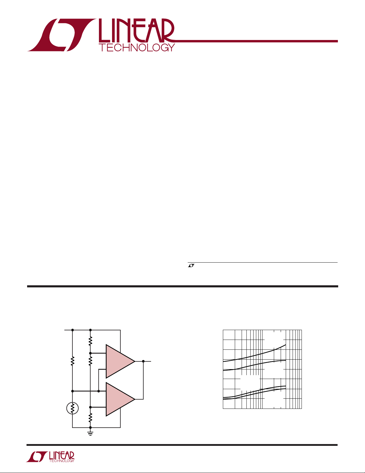
TYPICAL APPLICATIO
1.5V Powered Refrigerator Alarm
+
V
1.5V
665k
1%
3
+
1/2 LT1017
2
–
5
+
1/2 LT1017
6
–
YSI 44011
258.3k AT 5°C
333.1k AT 0°C
665k
1%
52.3k
1%
280k
1%
U
8
4
1017/18 TA01
1
7
OUTPUT HIGH FOR
0°C ≤ T ≤ 5°C
160
140
120
100
80
60
SUPPLY CURRENT (µA)
40
20
0
124
Supply Current
LT1018
OUTPUTS
LOW
LT1018
OUTPUTS
LT1017
OUTPUTS
LOW
TOTAL SUPPLY VOLTAGE (V)
HIGH
LT1017
OUTPUTS
HIGH
10 20 40 100
1017/18 TA02
10178fc
1
LT1017/LT1018
TOP VIEW
OUTPUT B
V
+
OUTPUT A
–IN A
–IN B
+IN B
+IN A
V
–
8
7
6
5
3
2
1
4
H PACKAGE
8-LEAD TO-5 METAL CAN
+
B
–
+
A
–
1
2
3
4
8
7
6
5
TOP VIEW
OUTPUT A
–IN A
+IN A
V
–
V
+
OUTPUT B
–IN B
+IN B
N8 PACKAGE
8-LEAD PDIP
+
B
–
+
–
A
TOP VIEW
SW PACKAGE
16-LEAD PLASTIC SO
1
2
3
4
5
6
7
8
16
15
14
13
12
11
10
9
NC
NC
OUT A
–IN A
+IN A
V
–
NC
NC
NC
NC
V
+
OUT B
–IN B
+IN B
NC
NC
A
W
O
LUTEXI TIS
S
A
WUW
U
(Note 1)
ARB
G
Supply Voltage ....................................................... 40V
Differential Input Voltage ........................................ 40V
Input Voltage ............................................ –0.3V to 40V
Short-Circuit Duration .................................... Indefinite
Storage Temperature Range ................ –65°C to 150°C
PACKAGE
/
O
RDER I FOR ATIO
WU
U
ORDER PART
NUMBER
LT1017MH
LT1017CH
LT1018MH
LT1018CH
T
= 150°C, θJA = 150°C/W, θJC = 45°C/W
JMAX
OBSOLETE PACKAGE
Consider the 8-Lead Plastic Dip Package for Alternate Source
ORDER PART
NUMBER
LT1017CS8
LT1017IS8
LT1018CS8
S8 PART
MARKING
1017
+IN A
1
–
V
2
+IN B
3
–IN B
4
S8 PACKAGE
8-LEAD PLASTIC SO
T
= 150°C, θJA = 190°C/W
JMAX
TOP VIEW
8
–IN A
OUT A
7
+
V
6
OUT B
5
1017I
1018
Consult LTC Marketing for parts specified with wider operating temperature ranges.
Operating Temperature Range
LT1017M/LT1018M ...................... –55°C to 125°C
LT1017C/LT1018C ............................... 0°C to 70°C
LT1017I........................................... –40°C to 85°C
Lead Temperature (Soldering, 10 sec)................. 300°C
ORDER PART
NUMBER
LT1017CN8
LT1017IN8
LT1018CN8
T
= 150°C, θJA = 130°C/W
JMAX
ORDER PART
NUMBER
LT1017CSW
LT1018CSW
T
= 150°C, θJA = 130°C/W
JMAX
LECTRICAL C CHARA TERIST
E
The ● denotes specifications which apply over the operating temperature
ICS
range of –55°C to 85°C for M grade parts, – 40°C to 85°C for I grade parts and 0°C to 70°C for C grade parts.
PARAMETER CONDITIONS MIN TYP MAX MIN TYP MAX UNITS
Offset Voltage ±0.75V ≤ VS ≤ ±20V 25°C 0.4 1 0.4 1 mV
(Note 2)
● 0.5 1.4 0.5 1.4 mV
125°C 5 0.7 1.5 mV
Bias Current ±0.75V ≤ VS ≤ ±20V 25°C 5 15 15 75 nA
● 7 25 18 100 nA
125°C 10 60 110 nA
Offset Current ±0.75V ≤ VS ≤ ±20V 25°C 0.4 2 1 8 nA
Common Mode Rejection Ratio VS = ±20V, – 20V ≤ VCM ≤ 19.1V 25°C 105 115 105 115 dB
2
● 0.5 3 1.6 12 nA
125°C20 20nA
● 100 115 100 115 dB
125°C 82 100 95 110 dB
LT1017 LT1018
10178fc
LT1017/LT1018
LECTRICAL C CHARA TERIST
E
The ● denotes specifications which apply over the operating temperature
ICS
range of –55°C to 85°C for M grade parts, – 40°C to 85°C for I grade parts and 0°C to 70°C for C grade parts.
PARAMETER CONDITIONS MIN TYP MAX MIN TYP MAX UNITS
Power Supply Rejection Ratio ±0.75V ≤ VS ≤ ±20V 25°C 96 110 96 110 dB
● 95 105 95 105 dB
125°C 82 86 100 dB
Gain No Load, V
RL = 4k, V
Output Sink Current V+ = 4.5V, V– = 0V 25°C3065 3570 mA
Overdrive > 30mV ● 25 50 25 50 mA
Output Source Current V+ = 40V, V– = 0V 25°C 30 75 75 250 µA
VIN = 5mV, V
V+ = 1.2V, V– = 0V 25°C 25 35 70 140 µA
VIN = 5mV, V
Negative Output Saturation I
Positive Output Saturation I
Leakage Current VS = 5V, V
Supply Current VS = 5V 25°C 30 60 110 250 µA
Minimum Operating Voltage I
Note 1: Absolute Maximum Ratings are those values beyond which the life
of the device may be impaired.
Note 2: Offset voltage is guaranteed over a common mode voltage range
of V– ≤ VIN ≤ (V+ – 0.9V).
= 0mA V+ = 4.5V, V– = 0V 25°C520 515mV
OUT
= 0.1mA VIN = –10mV 25°C 3560 3560 mV
= 1mA 25°C 60 120 60 120 mV
= 10mA 25°C 120 200 120 250 mV
= 30mA 25°C 350 600 350 700 mV
I
= 0mA V+ = 4.5V, V– = 0V ● 520 820 mV
OUT
= 0.1mA V
= 1mA ● 75 150 70 150 mV
= 10mA
= 30mA
I
= 0mA V+ = 4.5V, V– = 0V 125°C 2550 1040 mV
OUT
= 0.1mA V
= 1mA 125°C 100 200 110 200 mV
= 10mA 125°C 300 600 300 400 mV
= 30mA 125°C 900 mV
= 0µA25°C 4080 3580 mV
OUT
= 10µA25°C 175 250 175 250 mV
= 0µA
= 10µA ● 190 300 190 300 mV
= 0µA 125°C 50 100 50 100 mV
= 10µA 125°C 300 300 mV
≥ 100mV ● 0.6 3 1.8 10 µA
V
IN
VS = 40V 25°C 40 90 130 250 µA
= 1mA 25°C 1.15 1.2 V
OUT
= ±19.9V (Note 3) 25°C 110 115 110 125 dB
OUT
= ±19V 25°C 100 110 100 110 dB
OUT
= 0.4V ● 25 70 50 220 µA
OUT
= 0.4V ● 15 20 45 120 µA
OUT
= –10mV ● 40 75 35 70 mV
IN
= –10mV 125°C 60 100 60 100 mV
IN
= 40V 25°C 0.5 3 1 8 µA
OUT
● 105 115 105 120 dB
125°C 100 100 dB
● 94 94 dB
125°C1020 1030 mA
125°C 25 75 50 200 µA
125°C 25 40 40 110 µA
● 150 300 150 300 mV
● 600 900 500 900 mV
● 45 90 45 90 mV
125°C5 15µA
● 40 80 110 250 µA
125°C 80 300 µA
● 55 100 140 270 µA
125°C 100 300 µA
● 1.15 1.2 V
125°C 1.15 1.2 V
Note 3: No load gain is guaranteed but not tested (LT1017 only).
LT1017 LT1018
10178fc
3
LT1017/LT1018
LPER
F
O
R
ATYPICA
UW
CCHARA TERIST
E
C
ICS
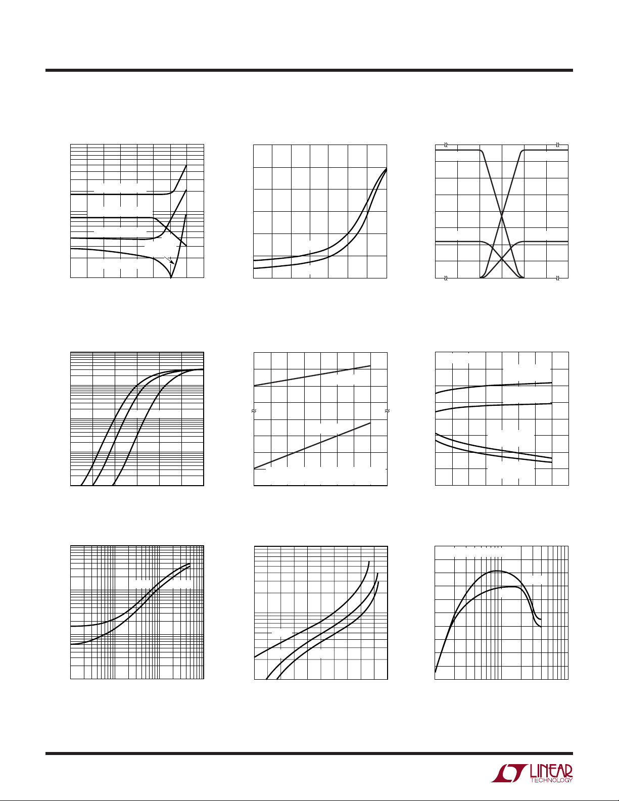
Input Bias Current
100
LT1018 VCM = V
LT1018 VCM = V+ – 1V
10
LT1017 VCM = V
INPUT BIAS CURRENT (nA)
LT1017 VCM = V+ – 1V
1
–50 –25
0
TEMPERATURE (°C)
–
–
REVERSES
POLARITY
50
25 75
I
BIAS
100
Input Bias Current with Inputs
Driven Below the Supply
100
10
125°C
–
0.2 –0.6 –1.0
COMMON MODE VOLTAGE (V)
INPUT BIAS CURRENT (µA)
1
0.1
0.01
85°C25°C
–0.2V
–0.8–0.4
125
1017/18 G01
1017/18 G04
150
Input Offset Current Bias Current vs Differential Input
3.0
2.5
2.0
1.5
1.0
INPUT OFFSET CURRENT (nA)
0.5
0
–50
–25 0
Common Mode Limits Supply Current
+
V
–0.4
–0.6
–0.8
–1.0
–
V
–0.2
–0.4
COMMON MODE VOLTAGE (V)
–0.6
∆VOS = 0.5mV
VOLTAGES ARE REFERRED TO SUPPLIES
–0.8
–50 –25 25 50 75
LT1018
LT1017
50 100 125
25 75
TEMPERATURE (°C)
VCM LOW
0
TEMPERATURE (°C)
VCM HIGH
100 125
1017/18 G02
150
1017/18 G05
20
LT1018 + I
B
15
10
LT1017 + I
BIAS CURRENT (nA)
5
0
–20
160
V
140
120
100
80
60
SUPPLY CURRENT (µA)
40
20
0
–50 –25 25 50 75
B
–0.2 –0.1 0.1
DIFFERENTIAL INPUT VOLTAGE (V)
= 20V
SUPPLY
0
TEMPERATURE (°C)
0
LT1018
OUTPUTS LOW
LT1018
OUTPUTS HIGH
LT1017
OUTPUTS LOW
LT1017
OUTPUTS HIGH
LT1018 – I
LT1017 – I
0.2
1017/18 G03
100 125
1017/18 G06
B
B
20
150
Positive Supply Current
10000
1000
100
POSITIVE SUPPLY CURRENT (µA)
10
0.1
OUTPUT SINK CURRENT (mA)
4
LT1018 LT1017
1 10 100
1017/18 G07
NPN Output Saturation Voltage Output Sinking Current Limit
1000
100
125°C
SATURATION VOLTAGE (mV)
10
0.001
0.01 1001010.1
SINK CURRENT (mA)
–55°C25°C
1017/18 G08
100
OUTPUT SHORTED TO V
80
60
40
20
OUTPUT CURRENT LIMIT (mA)
0
1
TOTAL SUPPLY VOLTAGE (V)
LT1017
10 100
+
LT1018
1017/18 G09
10178fc

LPER
F
O
R
ATYPICA
UW
CCHARA TERIST
E
C
LT1017/LT1018
ICS
Output Sinking Current Limit Total Switching Time
100
OUTPUT SHORTED TO V
LT1018
80
60
40
20
OUTPUT CURRENT LIMIT (mA)
0
–50
= 5V
V
S
LT1017
= 5V
V
S
V
V
–25 25
0
TEMPERATURE (°C)
LT1018
= 40V
S
LT1017
= 40V
S
+
125
50
100
75
150
1017/18 G10
100
RL = 47k (LT1018)
R
V
V
10
TOTAL SWITCHING TIME (µs)
1
–50
= 200k (LT1017)
L
= 90% V
OUT
OVERDRIVE
–25
FINAL
= 5mV
LT1018
FALL
LT1018
RISE
0
TEMPERATURE (°C)
25 75
Transition Time Positive Transition Time
100
10% V
V
10
TRANSITION TIME (µs)
1
0
≤ V
= 10mV
10
≤ 90% V
OUT
LT1017 RISE
LT1017 FALL/
LT1018 RISE
LT1018 FALL
20
FINAL
OVERDRIVE
TOTAL SUPPLY VOLTAGE (V)
FINAL
30
40
1017/18 G13
10
LT1017
= 2V
V
SUP
LT1017
= 40V
V
SUP
1
TRANSITION TIME (µs)
10% V
V
0.1
1k
OVERDRIVE
10k
PULL-UP RESISTOR (Ω)
FINAL
50
≤ V
= 10mV
100k
LT1017
FALL
LT1017
RISE
≤ 90% V
OUT
100
LT1018
V
SUP
LT1018
V
SUP
125
1017/18 G11
= 40V
= 2V
FINAL
1M
1017/18 G14
150
Output Delay
100
LT1017
RISE
10
DELAY TIME (µs)
1
0.1
V
OUT
LT1018
= 10% V
LT1017
FALL
LT1018
FALL
RISE
FINAL
1 10 100
OVERDRIVE (mV)
LT1017 Response Time
V
IN
RL = 10k
V
RL = 100k
OUT
V+ = 5V 5µs/DIV 1017/18 G15
V– = 0V
= 100mV STEP
V
IN
= 10mV
V
OVERDRIVE
1017/18 G12
5V
= ∞
R
L
0V
LT1017 Response Time LT1018 Response Time
V
IN
V
OUT
V+ = 5V 5µs/DIV 1017/18 G17
V– = 0V
= –100mV STEP
V
IN
= –10mV
V
OVERDRIVE
V
IN
R
= 10k
L
V
5V
0V
RL = 100k
OUT
V+ = 5V 2µs/DIV 1017/18 G16
V– = 0V
V
= 100mV STEP
IN
= 10mV
V
OVERDRIVE
LT1018 Response Time
V
5V
R
= ∞
L
0V
IN
V
OUT
V+ = 5V 2µs/DIV 1017/18 G18
V– = 0V
= –100mV STEP
V
IN
= –10mV
V
OVERDRIVE
5V
0V
10178fc
5

LT1017/LT1018
4
1017/18 TA03
8
2
3
5V
12V
V
IN
1
–
+
LT1017
PPLICATITYPICAL
O
U
SA
10k
V
IN
Driving Relays
LT1018 Op Amp, AV = 100
5V
3
2
10k 15Ω
+
LT1018
–
8
1
4
–5V
1M
R1*
0.22µF
1017/18 TA06
Increasing Positive Output Current Delay On Power Up
V
IN
V
OUT
R
L
R
= 100k
L
BANDWIDTH = 30Hz
–SLEW = 320V/ms
+SLEW = 0.93V/ms
*WITH R1 = 1k
BANDWIDTH ≅ 200Hz
3
2
+
LT1017/
LT1018
–
1µF100k
+
–
LT1017/
LT1018
+
V
8
4
1017/18 TA05
1
+
V
8
1
4
–
V
1N4148
2N3904
V
1017/18 TA04
OUT
+
3
2
20k1k
LT1017 Op Amp, AV = 100
10k
V
IN
5V
3
2
10k 10Ω
+
LT1017
–
8
1
4
–5V
1M
1017/18 TA07
V
OUT
RL ≥ 200k
–SLEW = 23.5V/ms
3.3µF
+SLEW = 0.017V/ms
BANDWIDTH = 0.3Hz AT R
= 220k
L
Negative Voltage Regulator
510k
LT1004
2.5V
6
100k
2
3
1k
–
LT1017/
LT1018
+
220pF
8
4
150pF
510k
1
220µF
+
1017/18 TA08
V
OUT
–5V
50mA
–V
IN
–5.2V TO
–40V
V
IN
0.01µF
V
IN
3
2
3
2
+
LT1018
–
+
LT1017/
LT1018
–
2-Wire Comparator
8
4
LT1018 ONLY
8
4
1
1
1N4148 ×2
1N4148 ×4
3V ≤ V
3V ≤ V
4.7k
4.7k
SUPPLY
SUPPLY
V
SUPPLY
OUTPUT
≤ 40V
V
SUPPLY
OUTPUT
≤ 40V
1017/18 TA09
10178fc

LT1017/LT1018
U
O
LT1034
1.235V
SA
5V Power Supply Monitor
+
V
36.5k
3k
1%
2.5k
1%
11.2k
1%
5
+
1/2 LT1017
6
–
3
+
1/2 LT1017
2
–
8
4
1017/18 TA10
7
1
OUTPUT VALID
+
FOR V
OUTPUT HIGH FOR
4.5V ≤ V
≤ 5.5V
IN
≥ 1.1V
PPLICATITYPICAL
LT1009
2.5V
Precise Tri-Wave Generator
1
7
TRIANGLE WAVE
OUTPUT
0.5V TO 2.5V
SQUARE WAVE
OUTPUT
5V
22k
0.047µF
3k
–
2
3
8
1/2 LT1013
+
4
100k
1
2N3904
200k
47k
22k
3k
3
+
2
–
5
+
6
–
8
1/2 LT1018
10pF
1/2 LT1018
4
1017/18 TA11
10178fc
7

LT1017/LT1018
PPLICATITYPICAL
O
U
SA
Power Supply Monitor
160k
V
IN
330Ω
1N4148
1M2M
LT1004
1.2V
110k
LT1004
2
–
1/2 LT1018
3
+
100k
+
1µF
1.2V
390k
1N4148
120k
1.5V Input Flyback Regulator
1.5V
100k 220pF
1
1N4148
1M
100k
0.0022µF
L1: RL1123-4.7-RENCO, INC
80% EFFICIENCY AT 2mA OUTPUT
1%
FILM
120k
FILM
2
3
1%
8
–
LT1018
+
4 0.01µF
V
IN
6.00V
5.25V
5.00V
4.75V
6
5
56.2k
1%
FILM
1
LED
OFF
FLASH AT 1Hz
FLASH AT 3Hz
FLASH AT 5Hz
–
1/2 LT1018
+
1% FILM
120k
1017/18 TA12
8
4
365k
1N4148
22µF
+
L1
4.7mH
7
HP5082-2810
OUTPUT
5V
+
47µF
1017/18 TA13
8
10178fc

LT1017/LT1018
U
O
PPLICATITYPICAL
SA
Regulated Step-Up Converter
5V
INPUT
0V TO 1V
LT1004
5
+
1/2 LT1018
6
–
FULL-SCALE
TRIM
100k
1.2V
100k
200k
7
*V
**DALE TE-5/Q3/400mH
Low Power* V-to-F Converter
910K
1%
2N3904
1N4148
2
0.1µF
3
1 +
= 1.2
OUT
()
1N4148
1N4148
0.1µF
–
1/2 LT1018
+
R1
R2
47k
2
–
1/2 LT1018
3
+
8
1
4
2000pF
0.001µF
POLYSTYRENE
8
4
1N4148
3M
1
400mH**
R1*
910k
R2*
120k
1N4148
+
1017/18 TA14
OUTPUT
10V
2mA
100µF
220k
1N4148
OUTPUT
0kHz TO 1kHz
9V
2.2µF
+
*I
100k
Q
1N4148
≅ 350µA
1M
10k 330k
7
220pF
1/2 LT1018
6
–
0.1µF
5
+
LT1034
1.2V
1017/18 TA15
10178fc
9

LT1017/LT1018
PACKAGEDESCRIPTI
0.335 – 0.370
(8.509 – 9.398)
DIA
0.305 – 0.335
(7.747 – 8.509)
0.016 – 0.021**
(0.406 – 0.533)
SEATING
PLANE
0.010 – 0.045*
(0.254 – 1.143)
0.040
(1.016)
MAX
U
O
H Package
8-Lead TO-5 Metal Can (.200 Inch PCD)
(Reference LTC DWG # 05-08-1320)
0.050
(1.270)
MAX
*
LEAD DIAMETER IS UNCONTROLLED BETWEEN THE REFERENCE PLANE
AND 0.045" BELOW THE REFERENCE PLANE
**
FOR SOLDER DIP LEAD FINISH, LEAD DIAMETER IS
0.165 – 0.185
GAUGE
PLANE
(4.191 – 4.699)
0.500 – 0.750
(12.700 – 19.050)
REFERENCE
PLANE
(0.406 – 0.610)
0.016 – 0.024
OBSOLETE PACKAGE
45°TYP
0.027 – 0.034
(0.711 – 0.864)
0.110 – 0.160
(2.794 – 4.064)
INSULATING
STANDOFF
0.027 – 0.045
(0.686 – 1.143)
PIN 1
H8(TO-5) 0.200 PCD 1197
0.200
(5.080)
TYP
N8 Package
8-Lead PDIP (Narrow .300 Inch)
(Reference LTC DWG # 05-08-1510)
876
0.255 ± 0.015*
(6.477 ± 0.381)
12
0.300 – 0.325
(7.620 – 8.255)
0.065
(1.651)
0.009 – 0.015
(0.229 – 0.381)
+0.035
0.325
–0.015
+0.889
8.255
()
–0.381
*THESE DIMENSIONS DO NOT INCLUDE MOLD FLASH OR PROTRUSIONS.
MOLD FLASH OR PROTRUSIONS SHALL NOT EXCEED 0.010 INCH (0.254mm)
TYP
0.045 – 0.065
(1.143 – 1.651)
0.100
(2.54)
BSC
0.400*
(10.160)
MAX
3
5
4
0.130 ± 0.005
(3.302 ± 0.127)
0.125
(3.175)
MIN
0.018 ± 0.003
(0.457 ± 0.076)
0.020
(0.508)
MIN
N8 1098
10
10178fc

PACKAGEDESCRIPTI
U
O
S8 Package
8-Lead Plastic Small Outline (Narrow .150 Inch)
(Reference LTC DWG # 05-08-1610)
0.189 – 0.197*
(4.801 – 5.004)
7
8
LT1017/LT1018
5
6
0.228 – 0.244
(5.791 – 6.197)
0.010 – 0.020
(0.254 – 0.508)
0.008 – 0.010
(0.203 – 0.254)
*
DIMENSION DOES NOT INCLUDE MOLD FLASH. MOLD FLASH
SHALL NOT EXCEED 0.006" (0.152mm) PER SIDE
**
DIMENSION DOES NOT INCLUDE INTERLEAD FLASH. INTERLEAD
FLASH SHALL NOT EXCEED 0.010" (0.254mm) PER SIDE
×
°
45
0.016 – 0.050
(0.406 – 1.270)
0°– 8° TYP
SW Package
16-Lead Plastic Small Outline (Wide .300 Inch)
(Reference LTC DWG # 05-08-1620)
0.053 – 0.069
(1.346 – 1.752)
0.014 – 0.019
(0.355 – 0.483)
TYP
1
16
3
2
0.398 – 0.413*
(10.109 – 10.490)
15 1413121110 9
4
0.150 – 0.157**
(3.810 – 3.988)
0.004 – 0.010
(0.101 – 0.254)
0.050
(1.270)
BSC
SO8 1298
NOTE 1
2345
0.050
(1.270)
BSC
1
0.014 – 0.019
(0.356 – 0.482)
TYP
0.291 – 0.299**
(7.391 – 7.595)
0.010 – 0.029
(0.254 – 0.737)
0.009 – 0.013
(0.229 – 0.330)
NOTE:
1. PIN 1 IDENT, NOTCH ON TOP AND CAVITIES ON THE BOTTOM OF PACKAGES ARE THE MANUFACTURING OPTIONS.
THE PART MAY BE SUPPLIED WITH OR WITHOUT ANY OF THE OPTIONS
DIMENSION DOES NOT INCLUDE MOLD FLASH. MOLD FLASH SHALL NOT EXCEED 0.006" (0.152mm) PER SIDE
*
DIMENSION DOES NOT INCLUDE INTERLEAD FLASH. INTERLEAD FLASH SHALL NOT EXCEED 0.010" (0.254mm) PER SIDE
**
NOTE 1
Information furnished by Linear Technology Corporation is believed to be accurate and reliable.
However, no responsibility is assumed for its use. Linear Technology Corporation makes no represen-
× 45°
0.016 – 0.050
(0.406 – 1.270)
° – 8° TYP
0
0.093 – 0.104
(2.362 – 2.642)
6
tation that the interconnection of its circuits as described herein will not infringe on existing patent rights.
78
0.037 – 0.045
(0.940 – 1.143)
0.394 – 0.419
(10.007 – 10.643)
0.004 – 0.012
(0.102 – 0.305)
S16 (WIDE) 1098
10178fc
11

LT1017/LT1018
TYPICAL APPLICATION
INTERROGATE
PULSE
500µs
INPUT
300k
TRIP
ADJUST
2
3
–
1/2 LT1018
+
LT1004
1.2V
8
1
4
100k 100Ω
3k
+
100µF
U
Fully Isolated Limit Comparator
5V
1k
2N3906
1µF
+
2N3906
10k
2N3904
TRW
PC-550-32
4.7k
ALL GATES 74C02
INTERROGATE PULSE
OUTPUT PULSE
NO OUTPUT PULSE FOR V
20k
200pF
> V
V
IN
TRIP
< V
IN
TRIP
OUTPUT
RELATED PARTS
PART NUMBER DESCRIPTION COMMENTS
LT1011/LT1011A Voltage Comparators Improved LT111A, 0.5mV V
LT1020 Micropower Regulator and Comparator 40µA I
SUPPLY
, 125mA I
OUT
LTC1040 Dual Micropower Comparator 1.5µW (1Sample/Second), 0.5mV V
LT1120/LT1120A Micropower Regulator with Comparator 20µA I
SUPPLY
, 125mA I
OUT
and Shutdown
LT319A Dual Comparators 0.5mV V
LT1671 Single Supply Ground Sensing Comparator 450µA I
, 25mA I
OS(MAX)
, 60ns tPD, 0.8mV V
SUPPLY
OUT
LT1716 Micropower, 44V, SOT-23 Input Common Mode Range Extends from –5V to 44V from Negative Supply
Ground Sensing Comparator
OS(MAX)
, 25nA I
B(MAX)
, 3nA I
, 2.5V Reference Voltage
, Rail-to-Rail Input
OS(MAX)
, 2.5V Reference Voltage
, 80ns t
PD
OS
OS(MAX)
, 250ns t
PD(MAX)
12
Linear Technology Corporation
1630 McCarthy Blvd., Milpitas, CA 95035-7417
(408) 432-1900 ● FAX: (408) 434-0507
●
www.linear.com
10178fc
LT/TP 1002 1K REV C • PRINTED IN USA
LINEAR TECHNOLOGY CORPORATION 1989
 Loading...