

Datasheet LT1008S8, LT1008MH, LT1008IN8, LT1008CN8, LT1008CJ8 Datasheet (Linear Technology)
...
FEATURES
LT1008
Picoamp Input Current,
Microvolt Offset,
Low Noise Op Amp
U
DESCRIPTIO
■
Guaranteed Bias Current
TA = 25°C: 100pA Max
TA = –55°C to 125°C: 600pA Max
■
Guaranteed Offset Voltage: 120µV Max
■
Guaranteed Drift: 1.5µV/°C Max
■
Low Noise, 0.1Hz to 10Hz: 0.5µV
■
Guaranteed Low Supply Current: 600µA Max
■
Guaranteed CMRR: 114dB Min
■
Guaranteed PSRR: 114dB Min
■
Guaranteed Voltage Gain with 5mA Load Current
P-P
U
APPLICATIO S
■
Precision Instrumentation
■
Charge Integrators
■
Wide Dynamic Range Logarithmic Amplifiers
■
Light Meters
■
Low Frequency Active Filters
■
Standard Cell Buffers
■
Thermocouple Amplifiers
The LT®1008 is a universal precision operational amplifier
that can be used in practically all precision applications.
The LT1008 combines for the first time, picoampere bias
currents (which are maintained over the full –55°C to
125°C temperature range), microvolt offset voltage (and
low drift with time and temperature), low voltage and
current noise, and low power dissipation. Extremely high
common mode and power supply rejection ratios, and the
ability to deliver 5mA load current with high voltage gain
round out the LT1008’s superb precision specifications.
The all around excellence of the LT1008 eliminates the
necessity of the time consuming error analysis procedure
of precision system design in many applications; the
LT1008 can be stocked as the universal precision op amp.
The LT1008 is externally compensated with a single capacitor for additional flexibility in shaping the frequency
response of the amplifier. It plugs into and upgrades all
standard LM108A/LM308A applications. For an internally
compensated version with even lower offset voltage but
otherwise similar performance see the LT1012.
, LTC and LT are registered trademarks of Linear Technology Corporation.
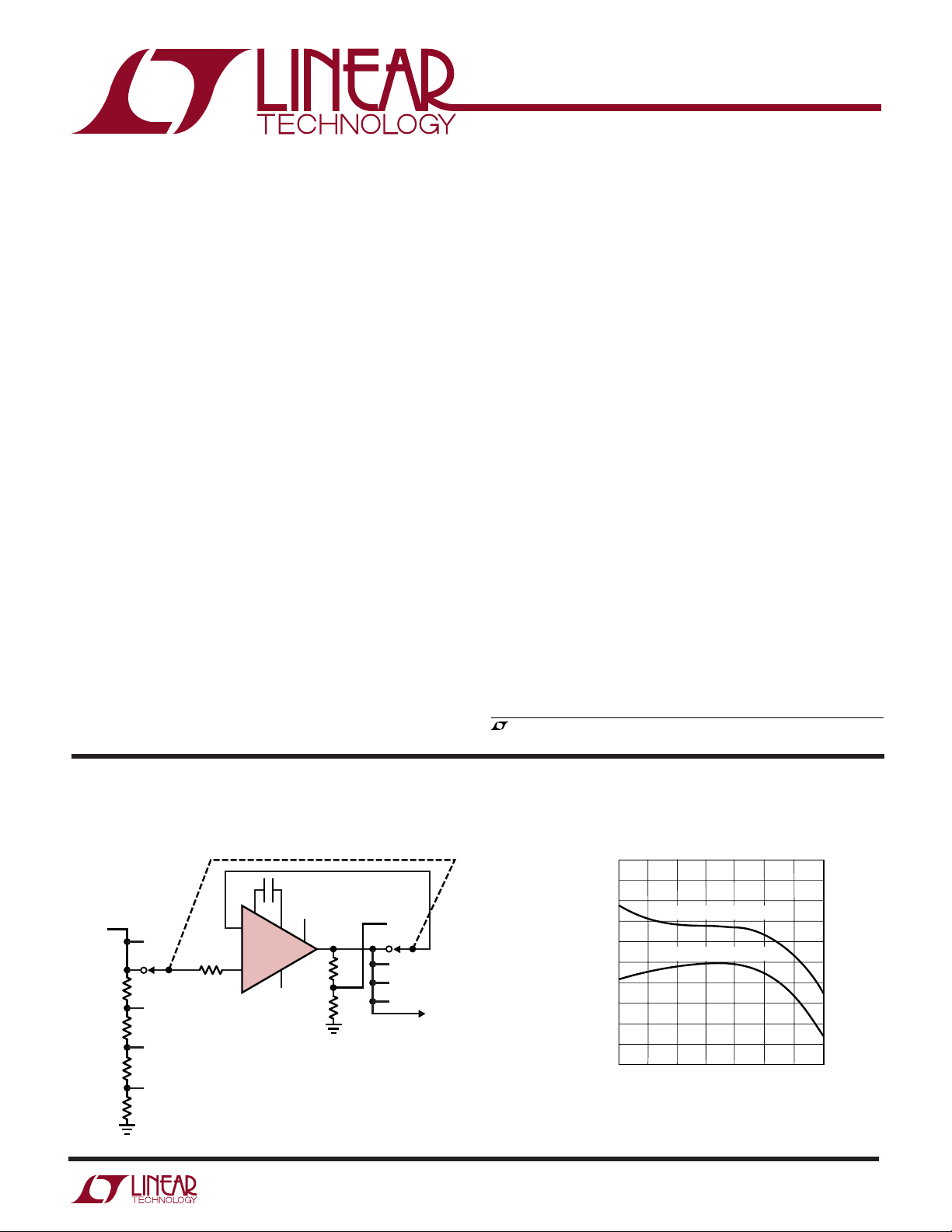
TYPICAL APPLICATIO
Input Amplifier for 4.5 Digit Voltmeter
1000pF
1
–
INPUT
1V
9M
900k
90k
10k
0.1V
10V
100V
1000V
100k
5%
FN507
ALLEN BRADLEY
DECADE VOLTAGE DIVIDER
2
3
8
LT1008
+
4
–15V
U
15V
7
6
9k*
1k*
*RATIO MATCH ±0.01%
THIS APPLICATION REQUIRES LOW
BIAS CURRENT AND OFFSET VOLTAGE,
LOW NOISE AND LOW DRIFT WITH
TIME AND TEMPERATURE
0.1V
1V
10V
100V
1000V
TO 1V FULL-SCALE
ANALOG-TO-DIGITAL
CONVERTER
1008 TA01
Input Bias Current vs Temperature
100
50
0
–50
INPUT BIAS CURRENT (pA)
–100
–150
–50
UNDERCANCELLED UNIT
OVERCANCELLED UNIT
25
0
–25
TEMPERATURE (°C)
50
75
100
125
1008 TA02
1
LT1008
1
2
3
4
8
7
6
5
TOP VIEW
COMP2
V
+
OUT
NC
COMP1
–IN
+IN
V
–
S8 PACKAGE
8-LEAD PLASTIC SO
WWWU
ABSOLUTE AXI U RATI GS
(Note 1)
Supply Voltage ...................................................... ±20V
Differential Input Current (Note 2) ..................... ±10mA
Input Voltage ........................................................ ±20V
Output Short-Circuit Duration......................... Indefinite
Storage Temperature Range ................. –65°C to 150°C
UU
W
PACKAGE/ORDER I FOR ATIO
TOP VIEW
COMP2
8
–
(CASE)
7
–
+
5
4
1
COMP1
2
–IN
+IN
3
V
H PACKAGE
8-LEAD TO-5 METAL CAN
T
= 150°C, θJA = 150°C/W, θJC = 45°C/W
JMAX
ORDER PART
NUMBER
+
V
6
OUT
NC
COMP1
1
–IN
2
+IN
3
–
V
4
N8 PACKAGE
8-LEAD PDIP
T
= 150°C, θJA = 130°C/W
JMAX
J8 PACKAGE 8-LEAD CERDIP
= 150°C, θJA = 100°C/W
T
JMAX
ORDER PART
NUMBER
Operating Temperature Range
LT1008M (OBSOLETE) ............... –55°C to 125°C
LT1008C................................................. 0°C to 70°C
LT1008I ............................................. –40°C to 85°C
Lead Temperature (Soldering, 10 sec)..................300°C
TOP VIEW
COMP2
8
+
V
7
OUT
6
NC
5
T
= 150°C, θJA = 190°C/W
JMAX
ORDER PART
NUMBER
ORDER PART
NUMBER
S8 PART
MARKING
LT1008MH
LT1008CH
OBSOLETE PACKAGES
Consider N8 or S8 Package for Alternate Source
Consult LTC Marketing for parts specified with wider operating temperature ranges.
ELECTRICAL CHARACTERISTICS
SYMBOL PARAMETER CONDITIONS MIN TYP MAX MIN TYP MAX UNITS
V
I
OS
I
B
e
i
n
A
2
OS
n
VOL
Input Offset Voltage 30 120 30 120 µV
Long-Term Input Offset Voltage Stability 0.3 0.3 µV/Month
Input Offset Current 30 100 30 100 pA
Input Bias Current ±30 ±100 ±30 ±100 pA
Input Noise Voltage 0.1Hz to 10Hz 0.5 0.5 µV
Input Noise Voltage Density fO = 10Hz (Note 4) 17 30 17 30 nV√Hz
Input Noise Current Density fO = 10Hz 20 20 fA/√Hz
Large-Signal Voltage Gain V
LT1008MJ8
LT1008CJ8
LT1008CN8
LT1008IN8
LT1008S8
1008
VS = ±15V, VCM = 0V, TA = 25°C, unless otherwise noted.
LT1008M/I LT1008C
(Note 3) 40 180 40 180 µV
(Note 4) 40 150 40 150 pA
(Note 5) ±40 ±150 ±40 ±150 pA
= 1000Hz (Note 5) 14 22 14 22 nV/√Hz
f
O
= ±12V, RL ≥ 10k 200 2000 200 2000 V/mV
OUT
V
= ±10V, RL ≥ 2k 120 600 120 600 V/mV
OUT
P-P
LT1008
ELECTRICAL CHARACTERISTICS
SYMBOL PARAMETER CONDITIONS MIN TYP MAX MIN TYP MAX UNITS
CMRR Common Mode Rejection Ratio VCM = ±13.5V 114 132 114 132 dB
PSRR Power Supply Rejection Ratio VS = ±2V to ±20V 114 132 114 132 dB
Input Voltage Range ±13.5 ±14 ±13.5 ±14 V
V
I
OUT
S
Output Voltage Swing RL = 10k ±13 ±14 ±13 ±14 V
Slew Rate CF = 30pF 0.1 0.2 0.1 0.2 V/µs
Supply Current (Note 3) 380 600 380 600 µA
VS = ±15V, VCM = 0V, TA = 25°C, unless otherwise noted.
LT1008M/I LT1008C
The ● indicates specifications which apply over the full operating temperature range of –55°C ≤ TA ≤ 125°C for the LT1008M, –40°C
≤ TA ≤ 85°C for the LT1008I and 0°C ≤ TA ≤ 70°C for the LT1008C. VS = ±15V, VCM = 0V, unless otherwise noted.
LT1008M/I LT1008C
SYMBOL PARAMETER CONDITIONS MIN TYP MAX MIN TYP MAX UNITS
V
OS
I
OS
I
B
A
VOL
CMRR Common Mode Rejection Ratio VCM = ±13.5V ● 108 128 110 130 dB
PSRR Power Supply Rejection Ratio VS = ±2.5V to ±20V ● 108 126 110 128 dB
V
OUT
I
S
Input Offset Voltage ● 50 250 40 180 µV
(Note 3)
Average Temperature Coefficient of
Input Offset Voltage
Input Offset Current ● 60 250 40 180 pA
(Note 3)
Average Temperature Coefficient of
Input Offset Current
Input Bias Current ● ±80 ±600 ±40 ±180 pA
(Note 3)
Average Temperature Coefficient of
Input Bias Current
Large-Signal Voltage Gain V
Input Voltage Range ● ±13.5 ±13.5 V
Output Voltage Swing RL = 10k ● ±13 ±14 ±13 ±14 V
Supply Current ● 400 800 400 800 µA
= ±12V, RL ≥ 10k ● 100 1000 150 1500 V/mV
OUT
● 60 320 50 250 µV
● 0.2 1.5 0.2 1.5 µV/°C
● 80 350 50 250 pA
● 0.4 2.5 0.4 2.5 pA/°C
● ±150 ±800 ±50 ±250 pA
● 0.6 6 0.4 2.5 pA/°C
(LT1008S8 only) VS = ±15V, VCM = 0V, TA = 25°C, unless otherwise noted.
SYMBOL PARAMETER CONDITIONS MIN TYP MAX UNITS
V
OS
I
OS
I
B
e
n
Input Offset Voltage 30 200 µV
(Note 3) 40 250 µV
Long-Term Input Offset Voltage Stability 0.3 µV/Month
Input Offset Current 100 280 pA
(Note 3) 120 380 pA
Input Bias Current ±100 ±300 pA
(Note 3) ±120 ±400 pA
Input Noise Voltage 0.1Hz to 10Hz 0.5 µV
Input Noise Voltage Density fO = 10Hz (Note 5) 17 30 nV/√Hz
= 1000Hz (Note 5) 14 22 nV/√Hz
f
O
P-P
3
LT1008
ELECTRICAL CHARACTERISTICS
SYMBOL PARAMETER CONDITIONS MIN TYP MAX UNITS
i
n
A
VOL
CMRR Common Mode Rejection Ratio VCM = ±13.5V 110 132 dB
PSRR Power Supply Rejection Ratio VS = ±2V to ±20V 110 132 dB
V
OUT
I
S
Input Noise Current Density fO = 10Hz 20 fA/√Hz
Large-Signal Voltage Gain V
Input Voltage Range ±13.5 ±14 V
Output Voltage Swing RL = 10k ±13 ±14 V
Slew Rate CF = 30pF 0.1 0.2 V/µs
Supply Current (Note 3) 380 600 µA
(LT1008S8 only) VS = ±15V, VCM = 0V, TA = 25°C, unless otherwise noted.
= ±12V, RL ≥ 10k 200 2000 V/mV
OUT
= ±10V, RL ≥ 2k 120 600 V/mV
V
OUT
(LT1008S8 only) The ● indicates specifications which apply over the full operating temperature range of 0°C ≤ TA ≤ 70°C.
VS = ±15V, VCM = 0V, unless otherwise noted.
SYMBOL PARAMETER CONDITIONS MIN TYP MAX UNITS
V
OS
I
OS
I
B
A
VOL
CMRR Common Mode Rejection Ratio VCM = ±13.5V ● 108 130 dB
PSRR Power Supply Rejection Ratio VS = ±2.5V to ±20V ● 108 128 dB
V
OUT
I
S
Input Offset Voltage ● 40 280 µV
(Note 3)
Average Temperature Coefficient of ● 0.2 1.8 µV/°C
Input Offset Voltage
Input Offset Current ● 120 380 pA
(Note 3)
Average Temperature Coefficient of ● 0.4 4 pA/°C
Input Offset Current
Input Bias Current ● ±120 ±420 pA
(Note 3)
Average Temperature Coefficient of ● 0.4 5 pA/°C
Input Bias Current
Large-Signal Voltage Gain V
Input Voltage Range ● ±13.5 V
Output Voltage Swing RL = 10k ● ±13 ±14 V
Supply Current ● 400 800 µA
= ±12V, RL ≥ 10k ● 150 1500 V/mV
OUT
● 50 340 µV
● 140 500 pA
● ±140 ±550 pA
Note 1: Absolute Maximum Ratings are those values beyond which the life
of a device may be impaired.
Note 2: Differential input voltages greater than 1V will cause excessive
current to flow through the input protection diodes unless current limiting
resistors are used.
4
Note 3: These specifications apply for ±2V ≤ V
(±2.5V ≤ V
–13.5V ≤ V
Note 4: 10Hz noise voltage density is sample tested on every lot. Devices
100% tested at 10Hz are available on request.
Note 5: This parameter is tested on a sample basis only.
≤ ±20V over the temperature range) and
S
≤ 13.5V (for VS = ±15V).
CM
≤ ±20V
S
LT1008
COMMON MODE INPUT VOLTAGE (V)
–15
–60
INPUT BIAS CURRENT (pA)
–40
–20
0
20
60
–10
–5 0 5
1008 G03
10 15
40
+
–
I
B
V
CM
DEVICE WITH POSITIVE INPUT CURRENT
DEVICE WITH NEGATIVE INPUT CURRENT
V
S
= ±15V
T
A
= 25°C
R
INCM
= 2 × 10¹²Ω
U
W
UU
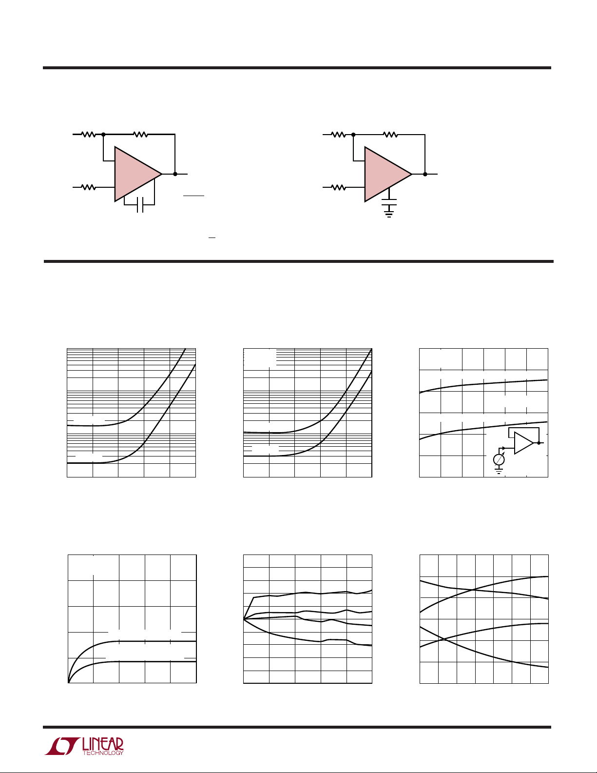
FREQUE CY CO PE SATIO CIRCUITS
Standard Compensation Circuit Alternate* Frequency Compensation
–V
IN
+V
IN
R1 R2
–
2
R3
LT1008
3
+
1
C
**BANDWIDTH AND SLEW RATE
ARE PROPORTIONAL TO 1/C
6
V
8
**
F
OUT
R1C
O
C
≥
F
R1 + R2
C
= 30pF
O
1008 FCC01
R2
FOR > 200, NO EXTERNAL FREQUENCY COMPENSATION IS NECESSARY
R1
F
–V
IN
+V
IN
R1 R2
UW
TYPICAL PERFOR A CE CHARACTERISTICS
Offset Voltage Drift vs Source
Resistance (Balanced or
Unbalanced)
100
Offset Voltage vs Source
Resistance (Balanced or
Unbalanced)
10
VS = ±15V
T
= 25°C
A
*IMPROVES REJECTION OF POWER
SUPPLY NOISE BY A FACTOR OF 5
–
2
8
**
C
S
100pF
6
LT1008
3
+
**BANDWIDTH AND SLEW RATE ARE
PROPORTIONAL TO 1/C
V
OUT
1008 FCC02
S
Input Bias Current vs
Common Mode Range
10
MAXIMUM
1
TYPICAL
0.1
1k 10k
OFFSET VOLTAGE DRIFT WITH TEMPERATURE (µV/°C)
Warm-Up Drift
5
= ±15V
V
S
= 25°C
T
A
4
3
2
1
CHANGE IN OFFSET VOLTAGE (µV)
0
0
TIME AFTER POWER ON (MINUTES)
100k 1M 10M 100M
SOURCE RESISTANCE (Ω)
METAL CAN (H) PACKAGE
DUAL-IN-LINE PACKAGE
PLASTIC (N) OR CERDIP (J)
1
3
2
4
1008 G01
1008 G04
1
MAXIMUM
0.1
TYPICAL
INPUT OFFSET VOLTAGE (mV)
0.01
1k 10k
100k 1M 10M 100M
SOURCE RESISTANCE (Ω)
1008 G02
Offset Voltage Drift with
Long-Term Stability of Four
Representative Units
10
8
6
4
2
0
–2
–4
–6
CHANGE IN OFFSET VOLTAGE (µV)
–8
5
–10
1
0
TIME (MONTHS)
3
4
2
5
1008 G05
Temperature of Four
Representative Units
60
40
20
0
–20
OFFSET VOLTAGE (µV)
–40
–60
–50
–25 0
TEMPERATURE (°C)
50 100 125
25 75
1008 G06
5

LT1008
UW
TYPICAL PERFOR A CE CHARACTERISTICS
Supply Current vs Supply Voltage
500
450
400
SUPPLY CURRENT (µA)
350
300
0
0.1Hz to 10Hz Noise
TA = 25°C
= ±2V TO ±20V
V
S
NOISE VOLTAGE (400nV/DIV)
2
0
4
TIME (SECONDS)
25°C
125°C
–55°C
5
SUPPLY VOLTAGE (±V)
6
8
1008 G09
Output Short-Circuit Current vs Time
15
12
9
6
SOURCING
3
0
–3
–6
–9
SINKING
SHORT-CIRCUIT CURRENT (mA)
–12
–15
0
10
15
20
1008 G07
0.5
TIME FROM OUTPUT SHORT (MINUTES)
1.0
25°C
1.5
Noise Spectrum
1000
TA = 25°C
V
= ±2V TO ±20V
S
100
CURRENT NOISE
VOLTAGE NOISE
10
1/f CORNER
2.5Hz
CURRENT NOISE DENSITY (fA/√Hz)
VOLTAGE NOISE DENSITY (nV/√Hz)
1
10
1
10 100 1000
FREQUENCY (Hz)
1/f CORNER
120Hz
1008 G10
0.1
TOTAL NOISE DENSITY (µV/√Hz)
0.01
–55°C
125°C
125°C
25°C
–55°C
2.0
2.5
3.0
3.5
1008 G08
Total Noise vs Source Resistance
10
TA = 25°C
V
= ±2V TO ±20V
S
AT 10Hz
1
R
–
R
+
= 2R
R
S
AT 1Hz
AT 10Hz
2103104105106107108
10
RESISTOR NOISE ONLY
SOURCE RESISTANCE (Ω)
AT 1Hz
1008 G11
Voltage Gain vs Frequency
140
120
100
80
60
40
VOLTAGE GAIN (dB)
20
–20
0
0.01 0.1
CS = 100pF
C
1
10
FREQUENCY (Hz)
= 30pF
F
6
100
CF = 3pF
CS = 10pF
1k
10k
100k
1M
1008 G12
10M
Gain, Phase Shift vs Frequency
with Alternate Compensation
40
30
20
GAIN (dB)
10
PHASE MARGIN
0
WITH C
T
A
V
S
–10
0.01
= 10pF
C
S
C
= 25°C
= ±15V
GAIN
CS = 10pF
φ
GAIN
= 100pF
S
= 100pF = 56°
S
0.1 1 10
FREQUENCY (MHz)
φ
= 100pF
C
S
1008 G13
100
120
140
160
180
200
40
30
PHASE SHIFT (DEG)
20
GAIN (dB)
10
–10
Gain, Phase Shift vs Frequency
with Standard (Feedback)
Compensation
φ
= 30pF
C
F
φ
C
C
GAIN
= 30pF
C
F
PHASE MARGIN
0
WITH C
= 25°C
T
A
= ±15V
V
S
0.01
GAIN
= 3pF
F
= 30pF = 60°
F
0.1 1 10
FREQUENCY (MHz)
= 3pF
F
100
120
PHASE SHIFT (DEG)
140
160
180
200
1008 G14

UW
FREQUENCY (Hz)
0.1
POWER SUPPLY REJECTION RATIO (dB)
100
120
140
100 10k
1008 G17
80
60
110
1k 100k 1M
40
20
NEGATIVE
SUPPLY
VS = ±15V
T
A
= 25°C
POSITIVE
SUPPLY
C
F
= 30pF
POSITIVE
SUPPLY
C
S
= 100pF
TYPICAL PERFOR A CE CHARACTERISTICS
LT1008
Voltage Gain vs Load Resistance
10M
VS = ±15V
= ±10V
V
O
3M
1M
VOLTAGE GAIN
300k
100k
12 5
LOAD RESISTANCE (kΩ)
10 20
Large-Signal Transient Response
2V/DIV
AV = 1 20µs/DIV 1008 G18
CS = 100pF
–55°C
25°C
125°C
1008 G15
Common Mode Rejection
vs Frequency
140
120
100
80
60
40
20
COMMON MODE REJECTION RATIO (dB)
0
1
10 100
CF = 30pF
= 100pF
C
S
FREQUENCY (Hz)
10k 1M
1k 100k
Slew Rate
vs Compensation Capacitance
10
VS = ±15V
T
= 25°C
A
1
SLEW RATE (V/µs)
0.1
0
C
F
20 100806040
COMPENSATION CAPACITOR (pF)
Power Supply Rejection
vs Frequency
V
= ±15V
S
= 25°C
T
A
1008 G16
Large-Signal Transient Response
2V/DIV
C
S
AV = 1 20µs/DIV 1008 G20
CF = 30pF
108 G19
Small-Signal Transient Response
20mV/DIV
AV = 1 5µs/DIV 1008 G21
CS = 100pF
C
LOAD
= 100pF
Small-Signal Transient Response
20mV/DIV
AV = 1 5µs/DIV 1008 G22
CS = 100pF
= 600pF
C
LOAD
Small-Signal Transient Response
20mV/DIV
AV = 1 5µs/DIV 1008 G23
CF = 30pF
= 100pF
C
LOAD
7

LT1008
–
+
LT1008
6
V
O
2
3
*RESISTORS MUST HAVE LOW
THERMOELECTRIC POTENTIAL
THIS CIRCUIT IS ALSO USED AS
THE BURN-IN CONFIGURATION
FOR THE LT1008 WITH SUPPLY
VOLTAGES INCREASED TO ±20V
V
O
= 1000V
OS
100Ω*
50k*
50k*
7
4
15V
–15V
1008 AI02
i
enV
M
n
no
=
()
Ω×
2
2
12
820
40 100
–
/
WUUU
APPLICATIO S I FOR ATIO
Achieving Picoampere/Microvolt Performance
In order to realize the picoampere—microvolt level accuracy of the LT1008, proper care must be exercised. For
example, leakage currents in circuitry external to the op
amp can significantly degrade performance. High quality
insulation should be used (e.g., TeflonTM, Kel-F); cleaning
of all insulating surfaces to remove fluxes and other
residues will probably be required. Surface coating may be
necessary to provide a moisture barrier in high humidity
environments.
Board leakage can be minimized by encircling the input
circuitry with a guard ring operated at a potential close to
that of the inputs: in inverting configurations the guard
ring should be tied to ground, in noninverting connections
to the inverting input at Pin 2. Guarding both sides of the
printed circuit board is required. Bulk leakage reduction
depends on the guard ring width. Nanoampere level leakage into the compensation terminals can affect offset
voltage and drift with temperature.
COMPENSATION
+
V
8
OUTPUT
7
6
5
4
1
2
3
The LT1008 is specified over a wide range of power supply
voltages from ±2V to ±18V. Operation with lower supplies
is possible down to ±1.2V (two Ni-Cad batteries).
Test Circuit for Offset Voltage and Its Drift with Temperature
Noise Testing
The 0.1Hz to 10Hz peak-to-peak noise of the LT1008 is
measured in the test circuit shown. The frequency response of this noise tester indicates that the 0.1Hz corner
is defined by only one zero. The test time to measure 0.1Hz
to 10Hz noise should not exceed 10 seconds, as this time
limit acts as an additional zero to eliminate noise contributions from the frequency band below 0.1Hz.
A noise voltage density test is recommended when measuring noise on a large number of units. A 10Hz noise
voltage density measurement will correlate well with a
0.1Hz to 10Hz peak-to-peak noise reading since both
results are determined by the white noise and the location
of the 1/f corner frequency.
REFERENCE ONLY—OBSOLETE PACKAGE
Microvolt level error voltages can also be generated in the
external circuitry. Thermocouple effects caused by temperature gradients across dissimilar metals at the contacts to the input terminals can exceed the inherent drift of
the amplifier. Air currents over device leads should be
minimized, package leads should be short, and the two
input leads should be as close together as possible and
maintained at the same temperature.
Teflon is a trademark of Dupont Company
8
Current noise is measured in the circuit shown and calcu-
INPUTS
1008 AI01
lated by the following formula where the noise of the
source resistors is subtracted.
10k
10M*
10M*
2
100Ω
10M*
10M*
*METAL FILM
–
LT1008
3
+
6
e
no
1008 AI04
–
V
GUARD

WUUU
APPLICATIO S I FOR ATIO
0.1µF
100k
LT1008
0.1Hz to 10Hz Noise Test Circuit
10Ω
*DEVICE UNDER TEST
NOTE: ALL CAPACITOR VALUES ARE FOR
NONPOLARIZED CAPACITORS ONLY
–
LT1008*
+
VOLTAGE
GAIN: 50,000
2k
+
4.7µF
–
24.3k
Frequency Compensation
The LT1008 is externally frequency compensated with a
single capacitor. The two standard compensation circuits
shown earlier are identical to the LM108A/LM308A frequency compensation schemes. Therefore, the LT1008
operational amplifiers can be inserted directly into
LM108A/LM308A sockets, with similar AC and upgraded
DC performance.
External frequency compensation provides the user with
additional flexibility in shaping the frequency response of
the amplifier. For example, for a voltage gain of ten and
CF = 3pF, a gain bandwidth product of 5MHz and slew rate
of 1.2V/µs can be realized. For closed-loop gains in excess
of 200, no external compensation is necessary, and slew
rate increases to 4V/µs. The LT1008 can also be overcom-
pensated (i.e., CF > 30pF or CS > 100pF) to improve capacitive load handling capability or to narrow noise bandwidth.
In many applications, the feedback loop around the amplifier has gain (e.g., logarithmic amplifiers); overcompensation can stabilize these circuits with a single capacitor.
The availability of the compensation terminals permits the
use of feedforward frequency compensation to enhance
slew rate in low closed-loop gain configurations. The
inverter slew rate is increased to 1.4V/µs. The voltage
follower feedforward scheme bypasses the amplifier’s
gain stages and slews at nearly 10V/µs.
The inputs of the LT1008 are protected with back-to-back
diodes. Current limiting resistors are not used, because the
leakage of these resistors would prevent the realization of
picoampere level bias currents at elevated temperatures.
LT1001
100k
0.1µF
4.3k
2.2µF
22µF
110k
SCOPE
×1
= 1M
R
IN
1008 AI03
In the voltage follower configuration, when the input is
driven by a fast, large-signal pulse (>1V), the input protection diodes effectively short the output to the input during
slewing, and a current, limited only by the output shortcircuit protection, will flow through the diodes.
The use of a feedback resistor, as shown in the voltage
follower feedforward diagram, is recommended because
this resistor keeps the current below the short-circuit
limit, resulting in faster recovery and settling of the output.
Inverter Feedforward Compensation
C2
5pF
INPUT
2V/DIV
R1
10k
2
–
3
+
C1
500pF
5µs/DIV 1008 AI07
LT1008
1
R2
10k
8
R3
3k
1008 AI05
6
C3
10pF
V
OUT
9

LT1008
WUUU
APPLICATIO S I FOR ATIO
Follower Feedforward Compensation
30pF
10k
2
INPUT*
10k
–
LT1008
3
+
6
OUTPUT
8
5V/DIV
1000pF
*SOURCE RESISTANCE ≤15k FOR STABILITY
TYPICAL APPLICATIO S
10k*
INPUT
Amplifier for Bridge Transducers Saturated Standard Cell Amplifier
2
–
LT1008
3
+
1
30pF
U
15V
7
8
1008 AI06
330pF
6
4
–15V OUTPUT
Logarithmic Amplifier
Q1A
2N2979
15.7k
*1% FILM RESISTOR
LOW BIAS CURRENT AND OFFSET VOLTAGE OF THE LT1008
ALLOW 4.5 DECADES OF VOLTAGE INPUT LOGGING
Q1B
2N2979
1k
TEL. LABS
TYPE Q81
124k* 5.1k
–
100pF2k
6
LM107
2
3
+
5µs/DIV 1008 AI07
15V
LT1004C
1.2V
10
100k
100k
S2
LT1008
1
15V
7
6
4
8
–15V
R2
OUTPUT
R5
+
V
S1
T
100k
R1
T
100k
R3
510k
R4
510k
R2
R6
56M
56M
C1
30pF
1
2
–
LT1008
3
+
VOLTAGE GAIN ≈ 100
3
2
R1
1008 TA05
+
–
1000pF
2N3609
1.018235V
SATURATED
+
8
6
OUTPUT
1008 TA04
STANDARD
CELL #101
EPPLEY LABS
NEWPORT, R.I.
THE TYPICAL 30pA BIAS CURRENT OF THE LT1008 WILL
DEGRADE THE STANDARD CELL BY ONLY 1ppm/YEAR.
NOISE IS A FRACTION OF A ppm. UNPROTECTED GATE
MOSFET ISOLATES STANDARD CELL ON POWER DOWN

TYPICAL APPLICATIO S
Amplifier for Photodiode Sensor Five Decade Kelvin-Varley Divider Buffered by the LT1008
LT1008
U
R1
5M
1%
2
–
λ
S1
R2
5M
1%
LT1008
3
+
8
C1
100pF
6
V
OUT
OUTPUT
= 10V/µA
1008 TA06
The LT1008 integrator extends low frequency range. Total
dynamic range is 0.01Hz to 10kHz (or 120dB) with 0.01%
linearity.
Extended Range Charge Pump Voltage to Frequency Converter
15V
–15V
50k
OPTIONAL 0.01Hz TRIM
22M
15V
1.8k
15V
10V
KELVIN-VARLEY
00000 – 99999 + 1
(POLYSTYRENE)
100k
DIVIDER
ESI #DP311
APPROXIMATE ERROR DUE TO NOISE, BIAS CURRENT,
COMMON MODE REJECTION. VOLTAGE GAIN OF THE
AMPLIFIER IS 1/5 OF A LEAST SIGNIFICANT BIT
1000pF
2
3
–
LT1008
+
1
1000pF
7
4
8
–15V
6
OUTPUT
1008 TA07
V
0V TO 10V
1µF
IN
63.4k*
10k*
2
–
LT1008
3
+
8
100pF
22k
2
+
7
LT311A
–
1
*1% METAL FILM RESISTOR
ALL DIODES 1N4148
3
4
–15V
10k*
6
100k
750k
5pF
3
10k*
2
10k
LT1004C
1.2V
+
LM301A
–
15V
6
10k
1008 TA08
1k
LM329
FREQUENCY OUPUT
0.01Hz TO 10kHz
10k
15V–15V
11

LT1008
TYPICAL APPLICATIO S
U
Precision, Fast Settling, Lowpass Filter
INPUT
*OPTO-MOS SWITCH
TYPE OFM1A
THETA-J CORP
2k
15V
This circuit is useful where fast signal acquisition and high
10k
2
7
7
–15V
100Ω
–15V
4
8
4
–
3
+
15V
8
LT311A
LT311A
LT1008
#1
#2
1
1000pF
+
–
1
5
–
+
1
2
3
10k
3
2
6
8
FILTER CUT
IN ADJUST
1008 TA09
OUTPUT
1.5M
1µF
OPTO-MOS*
1k
15V
precision are required, as in electronic scales.
The filter’s time constant is set by the 2k resistor and the
1µF capacitor until comparator 1 switches. The time
constant is then set by the 1.5M resistor and the 1µF
capacitor. Comparator 2 provides a quick reset.
The circuit settles to a final value three times as fast as a
simple 1.5M-1µF filter with almost no DC error.
INPUT
10k*
15k
10k
2pF TO 8pF
10k*
2N4393
×2
10k
2
3
–15V
2
3
1
–
LT318A
+
1N4148 (4)
300pF
15V
–
LT1008
+
1
30pF
Fast Precision Inverters
INPUT
15V
5
7
6
OUTPUT
4
7
6
4
8
SLEW RATE = 100V/µs
–15V
SETTLING (10V STEP) = 5µs TO 0.01%
OFFSET VOLTAGE = 30µV
BIAS CURRENT DC = 30pA
*1% METAL FILM
10k*
10k
10k
2
3
1N4148 ×2
300pF
15V
–
LT1008
+
1
30pF
7
8
–15V
1000pF
6
4
10k
10k*
10pF
15V
2
3
FULL POWER BANDWIDTH = 2MHz
SLEW RATE AT 50V/µs
SETTLING (10V STEP) = 12µs TO 0.01%
BIAS CURRENT DC = 30pA
OFFSET DRIFT = 0.3µV/°C
OFFSET VOLTAGE = 30µV
*1% METAL FILM
–
LT318A
+
–15V
7
6
OUTPUT
4
1008 TA10
12

WW
SCHE ATIC DIAGRA
LT1008
–INPUT
2
+INPUT
3
–
V
4
Q7 Q8
Q5
Q9
Q10
Q22
Q24
COMP2
8
Q20
3k
J1
Q32
Q33
16k
Q35
3.3k 320Ω
20k
Q29
Q25
Q30
Q27
Q28
1.5k
Q40
3k
40Ω
Q26
Q37
Q38
Q41
330Ω
Q43
Q42
60Ω
70Ω
+
V
7
OUTPUT
6
COMP1
1
1.3k 4.2k
22k
22k
Q6
Q16
Q13
Q2
Q1
Q39
Q17
Q14
Q4
Q3
SSS
Q15
Q18 Q19
3.3k
4.8k4.3k
3.3k
Q11
50kS1.5k
Q12
Q21
3k
Q23
Q31
Q34
13

LT1008
PACKAGE DESCRIPTIO
0.335 – 0.370
(8.509 – 9.398)
DIA
0.305 – 0.335
(7.747 – 8.509)
0.016 – 0.021**
(0.406 – 0.533)
SEATING
PLANE
0.040
(1.016)
MAX
0.010 – 0.045*
(0.254 – 1.143)
*
LEAD DIAMETER IS UNCONTROLLED BETWEEN THE REFERENCE PLANE
AND 0.045" BELOW THE REFERENCE PLANE
**
FOR SOLDER DIP LEAD FINISH, LEAD DIAMETER IS
U
H Package
8-Lead TO-5 Metal Can (.200 Inch PCD)
(Reference LTC DWG # 05-08-1320)
0.050
(1.270)
MAX
(4.191 – 4.699)
GAUGE
PLANE
(12.700 – 19.050)
0.016 – 0.024
(0.406 – 0.610)
0.165 – 0.185
0.500 – 0.750
REFERENCE
PLANE
45°TYP
0.028 – 0.034
(0.711 – 0.864)
0.110 – 0.160
(2.794 – 4.064)
INSULATING
STANDOFF
0.027 – 0.045
(0.686 – 1.143)
PIN 1
H8(TO-5) 0.200 PCD 1197
0.200
(5.080)
TYP
8-Lead CERDIP (Narrow .300 Inch, Hermetic)
(Reference LTC DWG # 05-08-1110)
CORNER LEADS OPTION
(4 PLCS)
0.023 – 0.045
(0.584 – 1.143)
HALF LEAD
0.045 – 0.068
(1.143 – 1.727)
FULL LEAD
OPTION
0.300 BSC
(0.762 BSC)
0.008 – 0.018
(0.203 – 0.457)
NOTE: LEAD DIMENSIONS APPLY TO SOLDER DIP/PLATE
OR TIN PLATE LEADS
0° – 15°
OPTION
J8 Package
0.005
(0.127)
MIN
0.025
(0.635)
RAD TYP
0.045 – 0.065
(1.143 – 1.651)
0.014 – 0.026
(0.360 – 0.660)
0.405
(10.287)
MAX
87
12
65
3
4
0.220 – 0.310
(5.588 – 7.874)
0.015 – 0.060
(0.381 – 1.524)
0.100
(2.54)
BSC
0.200
(5.080)
MAX
0.125
3.175
MIN
J8 1298
14
OBSOLETE PACKAGES

PACKAGE DESCRIPTIO
U
N8 Package
8-Lead PDIP (Narrow .300 Inch)
(Reference LTC DWG # 05-08-1510)
0.255 ± 0.015*
(6.477 ± 0.381)
0.400*
(10.160)
MAX
876
LT1008
5
12
0.300 – 0.325
(7.620 – 8.255)
0.065
(1.651)
0.009 – 0.015
(0.229 – 0.381)
+0.035
0.325
–0.015
+0.889
8.255
()
–0.381
*THESE DIMENSIONS DO NOT INCLUDE MOLD FLASH OR PROTRUSIONS.
MOLD FLASH OR PROTRUSIONS SHALL NOT EXCEED 0.010 INCH (0.254mm)
TYP
0.045 – 0.065
(1.143 – 1.651)
0.100
(2.54)
BSC
S8 Package
8-Lead Plastic Small Outline (Narrow .150 Inch)
(Reference LTC DWG # 05-08-1610)
8
3
0.189 – 0.197*
(4.801 – 5.004)
7
6
4
0.130 ± 0.005
(3.302 ± 0.127)
0.125
(3.175)
MIN
0.018 ± 0.003
(0.457 ± 0.076)
5
0.020
(0.508)
MIN
N8 1098
0.228 – 0.244
(5.791 – 6.197)
1
0.010 – 0.020
(0.254 – 0.508)
0.008 – 0.010
(0.203 – 0.254)
*
DIMENSION DOES NOT INCLUDE MOLD FLASH. MOLD FLASH
SHALL NOT EXCEED 0.006" (0.152mm) PER SIDE
**
DIMENSION DOES NOT INCLUDE INTERLEAD FLASH. INTERLEAD
FLASH SHALL NOT EXCEED 0.010" (0.254mm) PER SIDE
Information furnished by Linear Technology Corporation is believed to be accurate and reliable.
However, no responsibility is assumed for its use. Linear Technology Corporation makes no representation that the interconnection of its circuits as described herein will not infringe on existing patent rights.
× 45°
0.016 – 0.050
(0.406 – 1.270)
0.053 – 0.069
(1.346 – 1.752)
0°– 8° TYP
0.014 – 0.019
(0.355 – 0.483)
TYP
3
2
0.150 – 0.157**
(3.810 – 3.988)
4
0.004 – 0.010
(0.101 – 0.254)
0.050
(1.270)
BSC
SO8 1298
15

LT1008
TYPICAL APPLICATIO
U
Ammeter measures currents from 100pA to 100µA with-
out the use of expensive high value resistors. Accuracy at
Ammeter with Six Decade Range
CURRENT
INPUT
Q1 TO Q4: RCA CA3146 TRANSISTOR ARRAY
CALIBRATION: ADJUST R1 FOR FULL SCALE
DEFLECTION WITH 1µA INPUT CURRENT
10k
15V
2
3
–
LT1008
+
1
0.01µF
7
8
–15V
4
6
PIN 13
CA3146
33k
100µA is limited by the offset voltage between Q1 and Q2
and at 100pA by the inverting bias current of the LT1008.
10k
15V
10nA
1µA
10µA
Q3
R1
2k
1.2k
549Ω
549Ω
549Ω
549Ω
549Ω
549Ω
LT1004C-1.2
1008 TA11
100µA
METER
Q1
Q4
100pA
RANGE 1nA
Q2
100nA
100µA
RELATED PARTS
PART NUMBER DESCRIPTION COMMENTS
LT1012 Picoamp Input Current, Microvolt Offset, Low Noise Op Amp Internally Compensated LT1008
LT1112 Dual Low Power, Precision, Picoamp Input Op Amp Dual LT1012
LT1880 SOT-23, Rail-to-Rail Output, Picoamp Input Current Precision Op Amp Single SOT-23 Version of LT1884
LT1881/LT1882 Dual and Quad Rail-to-Rail Output, Picoamp Input Precision Op Amps Dual/Quad C
LT1884/LT1885 Dual and Quad Rail-to-Rail Output, Picoamp Input Precision Op Amps Dual/Quad Faster LT1881/LT1882
1008fa LT/TP 0701 1.5K REV A • PRINTED IN THE USA
16
Linear Technology Corporation
1630 McCarthy Blvd., Milpitas, CA 95035-7417
(408) 432-1900 ● FAX: (408) 434-0507
●
www.linear.com
Stable
LOAD
LINEAR TECHNOLOGY CORPORATION 1991
 Loading...