


Linear Technology Corporation
1630 McCarthy Blvd.
Milpitas, CA 95035-7417
Tel: 408-432-1900
www.linear.com
WF08098KU
VOL 3
Telecom, Datacom and Industrial
Power Products
High Performance Analog ICs

02 C O N T E N T S
Contents
Page Description
Simplified DC/DC Conversion Block Diagrams
01 Isolated Block Diagram
02 Nonisolated Block Diagram
Hot Swap™/Ideal Diode Controllers
03 Overvoltage Protection Regulator and Inrush Current Limiter
04 – 05 Hot Swap Controllers
06–08 Ideal Diode Controllers
07 48V Fuse Monitor
Isolated DC/DC Conversion
09 – 10 Flyback Controllers
10 – 11 Forward Controllers/Smart Drivers
12 Demonstration Boards – Telecom/Datacom (18V to 75V)
13 Industrial Power Conversion (9V to 36V)
14 – 15 Push-Pull, Half- and Full-Bridge Controllers
Nonisolated DC/DC Conversion, Up to 100V Input
16 Buck and Boost High Voltage Controllers
17 Forward Controllers
®
18 Buck-Boost µModule
Regulators and Controllers
19 Monolithic Buck Regulators/Linear Regulators
20 MOSFET Drivers/Opto Drivers/Reference Voltage
PoE, Interface, System Monitoring and Control
21 Power over Ethernet Controllers
22 – 23 Rugged Serial Interface Transceivers
2
24 I
C and SMBus Buffers and Accelerators
25 Voltage Monitors and Supervisors
25 Pushbutton Controllers
26 Coulomb Counter/Battery Gas Gauge
2
27 High Voltage I
C Current and Voltage Monitor
28 Supply Trackers, Sequencers and Margining Controllers
Visit www.linear.com for our complete product offering.
Isolated DC/DC Conversion
B L O C K DI A G RA MI S O L AT ED DC / D C CO N V E R S IO N 01
Surge Suppression, Hot Swap
Controllers – High Voltage
page 3 – 4
V
IN
(4V - 100V)
Fuse Monitor
page 7
Flyback Controllers
page 9 – 10
Forward Controllers/
Smart Drivers
page 10 – 11
Push-Pull,
Half- and Full-Bridge
Controllers
page 14 – 15
MOSFET Drivers
ORing Diode Controllers –
High Voltage
page 6, 7
Secondary-Side
Forward Controllers
page 10 – 11
Secondary-Side
Smart Drivers
page 11
Optocoupler Driver
Reference Voltage
page 20
0.6V to 52V
Optional IBA for
Point-of-Load (POL)
(Eg, 28V, 12V, 5V or 3.3V)
ORing Diode Controllers –
Low Voltage
page 8
–
LDO Regulators
Monolithic
Synchronous Buck
Regulators
µModule
Regulators
High Current Step
Down Controllers
1
®
1
Hot Swap Controllers –
Low Voltage
page 5
1
–
1
Load
Load
Load
Load
Load
Load
page 20
Power over Ethernet
Controllers
page 21
RS485/RS422 and
RS232 Transceivers
page 22, 23
1
For descriptions of these products, visit www.linear.com.
Multiple Output
Regulators
PolyPhase® Step
Down Controllers
Bus Buffers and Accelerators
System Monitor and Control,
Digital Power
page 24 page 25 – 28
1
–
1
Load
Load
0202 N O N I S O L AT ED DC / D C CO N V ER S I O N
Nonisolated DC/DC Conversion
B L O C K D IA G R A M
Surge Suppression, Hot Swap
Controllers – High Voltage
page 3, 4
V
IN
(4V - 100V)
Fuse Monitor
page 7
Buck Controllers
page 16
Forward Controllers
page 17
Buck-Boost µModule
Regulators and Controllers
page 18
ORing Diode Controllers –
High Voltage
page 6, 7
0.6V to 52V
Optional IBA for
Point-of-Load (POL)
(Eg, 28V, 12V, 5V or 3.3V)
ORing Diode Controllers –
Low Voltage
page 8
LDO Regulators
Monolithic
Synchronous Buck
1
Regulators
µModule
1
Regulators
Hot Swap Controllers –
Low Voltage
page 5
1
Load
Load
Load
Load
Load
Monolithic Buck Regulators
page 19
High Voltage LDOs
page 19
RS485/RS422 and
RS232 Transceivers
page 22, 23
1
For descriptions of these products, visit www.linear.com.
High Current Step
Down Controllers
Multiple Output
Regulators
PolyPhase Step
Down Controllers
System Monitor and ControlBus Buffers and Accelerators
page 24 page 25 – 28
–
1
1
–
1
Load
Load
Load
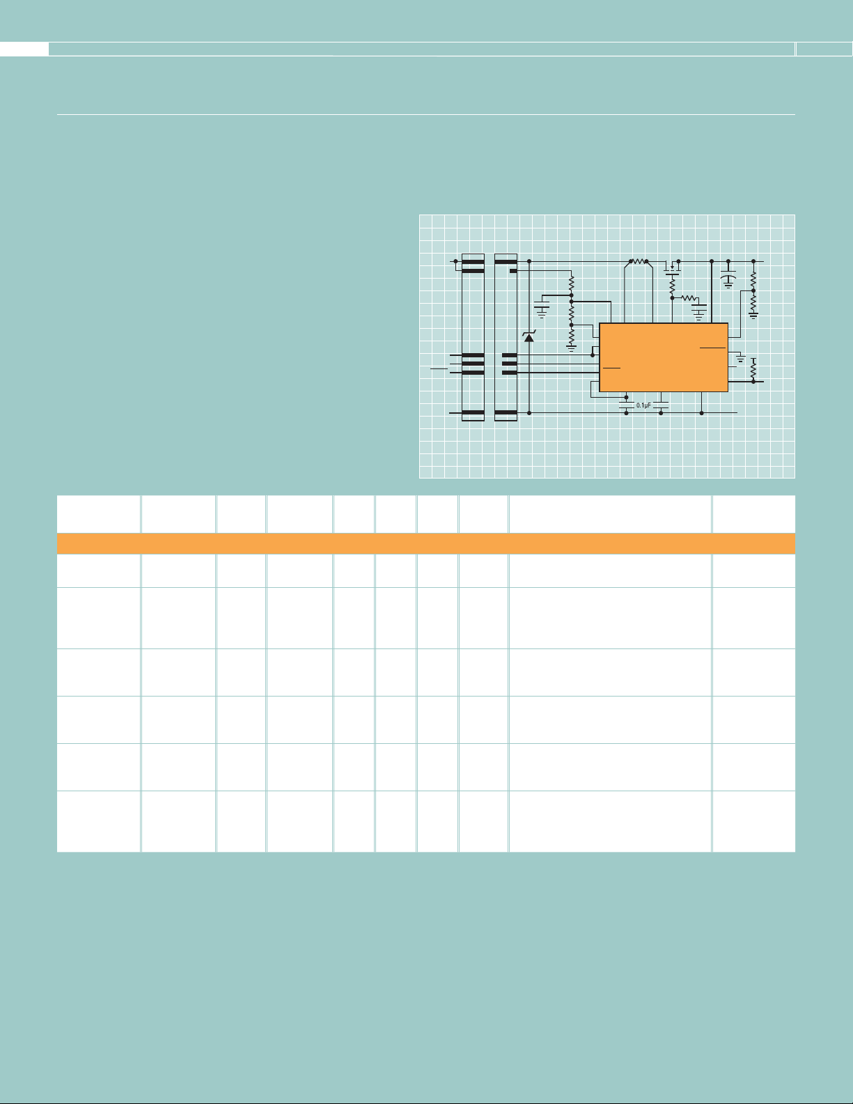
LT4356 Surge Stopper: Overvoltage Protection Regulator and Inrush Current Limiter
In industrial applications, high voltage power supply spikes with durations ranging from a few microseconds to hundreds of milliseconds
are commonly encountered. The electronics in these systems must not only survive transient voltage spikes, but in many cases also
operate reliably throughout the event.
®
The LT
voltage circuitry from damaging spikes and surges found in industrial systems. The LT4356 offers complete front end protection, guards
against overloads and short circuits, and withstands input voltage reversal with a simple IC/MOSFET solution. The LT4356 also protects
against DC overvoltage and overcurrent, which ordinary surge suppressors cannot do.
Under normal conditions, the LT4356 drives the MOSFET fully on, so that input power passes through directly to the load, with very little
loss. If the input voltage rises above an adjustable output threshold, the LT4356 regulates the output at a safe level. The regulating action
eliminates the need to use high voltage rated components downstream. Instead, less costly components may be used, because the
LT4356 blocks high voltages from reaching them.
The LT4356 provides the ability to ride out transients for continued system operation. If the fault persists, an adjustable timer sets a time
limit to ensure the MOSFET stays within its operating limits before the load is disconnected and the system is shut down. The timer
capacitor is charged with a current proportional to the voltage drop, Vds. For an overcurrent fault, the timer charging current is increased.
This unique feature takes more advantage of the Safe Operating Area (SOA) of the MOSFET than would a fixed timer interval, allowing the
user to size the MOSFET appropriately for their surge requirements.
4356 Surge Stopper reduces the need for bulky filtering components (capacitors, inductors, TVS diodes, fuses) by isolating low
0303O V E R V O LTA GE PR O T EC T I O N RE G U L AT OR A N D I N RU S H CU R R E N T LI M I TE R
03034 8 V I S O LAT ED CO N V E R S I O N
LT4356 Features:
•
Stops High Voltage Surges
•
Adjustable Output Clamp Voltage
•
Overcurrent Protection
•
Wide Operation Range: 4V to 80V
•
Reverse Input Protection to –60V
•
Low 7μA Shutdown Current, LT4356-1/LT4356-3
•
Adjustable Fault Timer
•
Inrush Current Limiting
•
Controls N-Channel MOSFET
•
Shutdown Pin Withstands –60V to 100V
•
Fault Output Indication
•
Spare Amplifier for Level Detection Comparator or Linear Regulator Controller
•
Guaranteed Operation to 125ºC
•
Latchoff Operation (LT4356-3)
•
Automatic Retry (LT4356-1, LT4356-2)
•
Available in (4mm × 3mm) 12-Pin DFN, 10-Pin MSOP or 16-Pin SO Packages
4A, 12V Overvoltage Output Regulator
10mΩ
IRLR2908
LT4356DE
GND TMR
12V
V
383k
100k
IN
V
CC
SHDN
+
IN
A
OUT
V
OUT
10Ω
OUTGATESNS
0.1µF
Overvoltage Protection Regulates
Output at 27V During Transient
80V INPUT SURGE
102k
FB
4.99k
EN
FAULT
FLTUNDERVOLTAGE
V
CC
DC/DC
CONVERTER
SHDN
GND
20V/DIV
V
OUT
20V/DIV
V
IN
12V
27V CLAMP
12V
100ms/DIV
0204 H O T S W A P CO N T R OL L E R S – HI G H VO LTA GE
Hot Swap Controllers – High Voltage
Hot Swap controllers allow a circuit board to be safely inserted and removed from a live backplane. Using an N-channel pass MOSFET,
the board supply voltage can be ramped at an adjustable rate. Product features include independent adjustable inrush current and
overcurrent limits to minimize stresses on the pass MOSFET during start-up, input step, and output step short-circuit conditions. Newer
generation devices include an onboard ADC for board voltage and current monitoring, and an I
®
LTC
4260: Positive High Voltage Hot Swap Controller
2
C Compatible Monitoring
with I
Features:
•
Allows Safe Insertion into Live Backplane
•
8-Bit ADC Monitors Current and Voltage
•
I2C/SMBus Interface
•
Wide Operating Voltage Range: 8.5V to 80V
•
High Side Drive for External N-Channel MOSFET
•
Input Overvoltage/Undervoltage Protection
•
Optional Latchoff or Autoretry After Faults
•
Alerts Host After Faults
•
Foldback Current Limiting
3A, 48V Card Resident Application
48V
CONNECTOR 1
CONNECTOR 2
SDA
SCL
ALERT
GND
BACKPLANE PLUG-IN
*DIODES INC. SMBT70A
CARD
2
C interface for microcontroller interaction.
0.010Ω
FDB3632
49.9k
0.1μF
1.74k
UV
2.67k
*
OV
SDAO
SDAI
SCL
ALERT
ON
V
INTV
DD
SENSE
LTC4260
CC
10Ω
100k
6.8nF
GATE
TIMER GND
68nF
SOURCE
BD_PRST
ADIN
GPIO
V
OUT
+
FB
48V, 3A
C
L
43.5k
3.57k
24k
Part Number
Input Voltage
Range
Inrush
Control
High Voltage Hot Swap Controllers
LT4250 –18V to –80V Ramp ACL
LTC4252A-1/2 –15V to –100V
(Floating)
Active or
Ramp
LT4256-1/2/3 10.8V to 80V Active or
Ramp
LTC4260 8.5V to 80V Active or
Ramp
LTC4261 –12V to –100V
Ramp ACL
(Floating)
LT4356-1/2/3 4V to 80V Active or
Ramp
1
ACL = Active Current Limit
Overcurrent
Control UV OV
ACL
ACL
ACL
ACL
1
1
1
1
1
1
Yes Yes Yes LT1640A Pin-Compatible with Active Current
Yes Yes Yes Soft-Start Limits Inrush dI/dt Drain Accelerated
Yes Yes Yes LT4256-1/2 Pin-Compatible Upgrade to
Yes Yes Yes Yes Onboard 8-Bit ADC for Card Voltage and
Yes Yes Yes Delayed Onboard 10-Bit ADC for Card Voltage and
Fault
PWRGD/
Output
Reset Description Package
Limiting
Response. ±1% Undervoltage/Overvoltage
Threshold Accuracy for AdvancedTCA
Applications
LT1641. Open Circuit Detect Output. Latchoff/
Auto-Retry Operation
Current Monitoring, I2C Interface. Programmable
Latchoff or Auto-Retry
Current Monitoring, I2C Interface. Programmable
Latchoff or Auto-Retry
Yes Yes Surge Stopper: Overvoltage Protection
and Inrush Limiting. Spare Amplifier for
UV/OV Monitoring or Linear Regulator.
Latchoff/Auto-Retry Operation
SO-8
MSOP-8
MSOP-10
SO-8
SSOP-16
5x5 QFN-32
SSOP-24
SO-24
4x5 QFN-24
SSOP-28
4x3 DFN-12
MSOP-10
SO-16

Hot Swap Controllers – Low Voltage
Low voltage Hot Swap controllers include independent high side gate drivers to control single or dual voltages, as well as voltage power-up
and power-down ramp control, current foldback and inrush limiting. Our latest LTC4217 and LTC4218 Hot Swap products allow the
current limit threshold to be adjusted dynamically using an external pin. Additional features include a current monitor output that amplifies
the sense resistor voltage for ground referenced current sensing and a MOSFET temperature monitor output. Dedicated 12V versions
contain preset 12V-specific thresholds.
0305H O T S W A P CO N T R OL L E R S – LO W VO LTA GE
LTC4215: Hot Swap Controller with
2
C Compatible Monitoring
I
Features:
•
Allows Safe Insertion into Live Backplane
•
8-Bit ADC Monitors Current and Voltage
•
I2C/SMBus Interface
•
Wide Operating Voltage Range: 2.9V to 15V
•
dI/dt Controlled Soft-Start
•
High Side Drive for External N-Channel MOSFET
•
No External Gate Capacitor Required
•
Input Overvoltage/Undervoltage Protection
•
Optional Latchoff or Auto-Retry After Faults
•
Alerts Host After Faults
•
Inrush Current Limit with Foldback
•
Available in 24-Lead (4mm × 5mm) QFN and
16-Lead Narrow SSOP Packages
Part Number Channels
Input Voltage
Range
Inrush
Control
Low Voltage Hot Swap Controllers
LTC4210-1/2/3/4 1 2.7V to 16.5V Active or
Ramp
LTC4211 1 2.5V to 16.5V Active or
Ramp
LTC4215-1/2/3 1 2.9V to 16.5V Active or
Ramp
LTC4216 1 0V to 6V Active or
Ramp
LTC4217/-12 1 2.9V to 26.5V Active or
Ramp
LTC4218/-12 1 2.9V to 26.5V Active or
Ramp
LTC4222 2 2.9V to 29V Active or
Ramp
LTC4223-1/2 2 10V to 14V
2.7V to 6V
1
ACL = Active Current Limit
2
ECB = Electronic Circuit Breaker
Active or
Ramp
Overcurrent
Control
1
ACL
2
ECB
1
ACL
1
ACL
1
ACL
1
ACL
1
ACL
1
ACL
12V Application with 5A Circuit Breaker
0.005Ω
12V
34.8k
0.1µF
1.18k
Fault
Output
PLUG-IN
CARD
P6KE16A
CONNECTOR 1
3.4k
INTV
0.1µF
SDA
ALERT
GND
CONNECTOR 2
SCL
BACKPLANE
PWRGD/
Reset Description Package
UV VDDSENSE+SENSE–GATE
OV
SDAO
SDAI
SCL
ALERT
CC
INTV
CC
LTC4215UFD
Yes Active Current Limiting with a Circuit Breaker.
FDC653N
10Ω
TIMER SSON GND
68nF
+
SOURCE
ADIN
GPIO
SOT-23
Latchoff/Auto-Retry Operation
Yes Delayed No Gate Capacitor Required SO-8
MSOP-8
MSOP-10
Yes Yes I2C/SMBus Interface, Internal 8-bit ADC, dI/dt
Controlled Soft-Start
Delayed Ultralow Voltage Hot Swap Controller for 0V to 6V,
with a Separate Supply of 2.3V to 6V. Adjustable
SSOP-16
4x5 QFN-24
MSOP-10
4x3 DFN-12
Current Limit, Soft-Start and Response Time for
Overcurrent Protection
Yes Yes Small Footprint 2A Hot Swap Controller. Integrated
33mΩ MOSFET and R
. Adjustable, 5%
SENSE
TSSOP-10
5x3 DFN-16
Accurate Current Limit. 2% Accurate Undervoltage
and Overvoltage Protection. A Dedicated
12V Version (LTC4217-12) Contains Preset
12V Specific Thresholds
Yes Yes Adjustable, 5% Accurate (15mV) Current Limit. 2%
Accurate Undervoltage and Overvoltage Protection.
SSOP-16
5x3 DFN-16
A Dedicated 12V Version (LTC4218-12) Contains
Preset 12V Specific Thresholds
Yes I2C/SMBus Interface, Internal 10-bit ADC, dI/dt
Controlled Soft-Start. Latchoff/Auto-Retry Operation
Yes Yes Controls 12V and 3.3V Auxiliary Supplies. Integrated
0.3Ω AUX Switch. Adjustable Current Limit with
5x5 QFN-32
SSOP-36
5x5 QFN-32
SSOP-36
Circuit Breaker. Latchoff/Auto-Retry Operation
V
OUT
12V
C
L
30.1k
3.57k
FB
INTV
EN
CC
24k
0206 I D E A L D IO D E CO N T R O L L ER S – H I GH V OLTA GE
ORing Ideal Diode Controllers
Linear’s family of ideal diode controllers reduces forward voltage drop and power dissipation in ORing applications, eliminating the
heat sinks required by conventional rectifiers. They deliver smooth switchover without chatter and are free from oscillation in load sharing
applications, yet respond quickly when called upon to block DC current in the reverse state. Our controllers prevent backfeeding between
supplies and are easily configured to protect against reverse polarity inputs.
Ideal Diode Controllers – High Voltage
LTC4354: Negative Voltage Diode-OR Controller and Monitor
The LTC4354 is a negative voltage and the LTC4355 is a positive voltage
diode-OR controller that drive two external N-channel MOSFETs. Each
replaces two Schottky diodes and the associated heat sink, saving power
and space. The power dissipation is greatly reduced by using N-channel
MOSFETs as the pass transistors. Power sources can be easily ORed
together to increase total system power and reliability.
LTC4355: Positive High Voltage Dual Ideal Diode-OR with Input
Supply and Fuse Monitors
The LTC4355 can diode-OR two positive supplies or the return paths
of two negative supplies, such as in a –48V system. Power fault
detection indicates if the input supplies are not in regulation, the
inline fuses are blown, or the voltages across the MOSFETs are
greater than the fault threshold.
Features:
•
Replaces Power Schottky Diodes
•
Controls N-Channel MOSFETs
•
0.5µs Turn-Off Time Limits Peak Fault Current
•
Wide Operating Voltage Range: 9V to 80V
•
Smooth Switchover without Oscillation
•
No Reverse DC Current
•
Monitors VIN, Fuse and MOSFET Diode
•
Available in 14-Lead (4mm × 3mm) DFN,
Positive and Negative Supply Diode-ORing
RTNA
RTNB
16-Lead MS and SO Packages
IN1 GATE1 IN2
LTC4355
LTC4355
GND
GATE2 OUT
Power Dissipation vs Load Current
6
5
DIODE (MBR10100)
4
3
2
POWER DISSIPATION (W)
1
0
0
FET (FDB3632)
2 4 6 8
CURRENT (A)
POWER
SAVED
10
LOAD
VA=-48V
VB=-48V
V
CC
LTC4354
LTC4354
DA
DB
GA GB
V
SS
0307I D E A L D IO D E CO N T R O L L ER S / F U S E MO N I T OR
LTC4357: Positive High Voltage Ideal Diode Controller
The LTC4357 easily ORs power sources to increase total
system reliability. In diode-OR applications, the LTC4357 controls
48V, 10A Diode-OR
V
INA
48V
FDB3632
the forward voltage drop across the MOSFET to ensure smooth
current transfer from one path to the other without oscillation.
If the power source fails or is shorted, a fast turn-off minimizes
reverse current transients.
Features:
•
Reduces Power Dissipation by Replacing a Power Schottky Diode
with an N-Channel MOSFET
•
0.5µs Turn-Off Time Limits Peak Fault Current
•
Wide Operating Voltage Range: 9V to 80V
•
Smooth Switchover without Oscillation
•
No Reverse DC Current
•
Available in 6-Lead (2mm × 3mm) DFN and 8-Lead MSOP Packages
V
48V
IN OUT
INB
IN OUT
GATE
LTC4357
GND
FDB3632
GATE
LTC4357
GND
V
DD
V
DD
V
OUT
Part Number Input Supply Range Ideal Diode External FET Fault Monitoring Package
High Voltage Ideal Diode Controllers
LTC4354 –4.5V to –100V (Floating) Dual N-Channel Yes 3x2 DFN-8, SO-8
LTC4355 9V to 80V Dual N-Channel Yes 4x3 DFN-14, SO-16,
MSOP-16
LTC4357 9V to 80V Single N-Channel No 2x3 DFN-6, MSOP-8
TO LOAD
48V Fuse Monitor
The LTC1921 monitors two independent –48V supplies, including their fuses and drives up to three optoisolators to indicate status.
Requiring only three noncritical resistors and optoisolators, the LTC1921 replaces multiple voltage comparators, a voltage reference and
several precision resistors.
Dual Supply Fuse Monitor
–48V
RETURN
SUPPLY A
–48V
SUPPLY B
–48V
100k
100k
RTN
V
A
V
B
FUSE A
FUSE B
F1
F2
LTC1921
LTC1921
OUT F
OUT A
OUT B
FUSE GOOD
SUPPLY A GOOD
SUPPLY B GOOD
LOGIC
SUPPLY
SUPERVISOR
µP
LOGIC
COMMON
–48V LOAD
Part Number Input Voltage Range UV OV Package
Fuse Monitor
LTC1921 –10V to –80V Yes Yes MSOP-8, SO-8

08 I D E A L D IO D E S AN D CO N T R O L LE R S – L OW V OLTA GE
Ideal Diodes and Controllers – Low Voltage
LTC4352: Low Voltage Ideal Diode Controller with Monitoring
The LTC4352 is a 0V to 18V ideal diode controller that enables low
loss ORing of multiple power sources with minimal disturbance to
supply voltages. A fast turn-on reduces the load voltage drop during
supply switchover. Power passage is disabled during undervoltage
or overvoltage conditions. The controller also features an open
MOSFET detect circuit that flags excessive voltage drop across the
pass transistor in the on state. A REV pin enables reverse current,
overriding the diode behavior when desired.
Features:
•
Low Loss Replacement for Power Diode
•
Controls N-Channel MOSFET
•
0V to 18V Supply ORing or Holdup
•
0.5μs Turn-On and Turn-Off Time
•
Undervoltage and Overvoltage Protection
•
Open MOSFET Detect
•
Status and Fault Outputs
•
Hot Swappable
•
Reverse Current Enable Input
•
12-Pin MSOP and DFN (3mm × 3mm) Packages
LTC4358: 5A Ideal Diode
The LTC4358 is a 5A ideal diode that uses an internal 20mΩ
N-channel MOSFET to replace a Schottky diode when used in
diode-OR and high current diode applications. The LTC4358
reduces power consumption, heat dissipation, and PC board area.
Features:
•
Replaces a Power Schottky Diode
•
Internal 20mΩ N-Channel MOSFET
•
0.5μs Turn-Off Time Limits Peak Fault Current
•
Operating Voltage Range: 9V to 26.5V
•
Smooth Switchover without Oscillation
•
No Reverse DC Current
•
Available in 14-Pin (4mm × 3mm) DFN and 16-Lead TSSOP Packages
Input Supply
Part Number
Range Ideal Diode External FET Package
5A Ideal Diode
LTC4352 0V to 18V Single, Fast Turn-On
and Turn-Off
LTC4358 9V to 28V Single Internal 5A
N-Channel 3x4 DFN-12
MSOP-12
4x3 DFN-14
FET
TSSOP-16
LTC4412 2.5V to 28V Single P-Channel ThinSOT ™
LTC4412HV 2.5V to 36V Single P-Channel ThinSOT
LTC4414 3V to 36V Single P-Channel MSOP-8
12V Ideal Diode with Status and Fault Indicators
Q1
IN
LTC4352
GND
POWER DISSIPATION (W)
LTC4358
GND
LTC4358
GND
Si7336ADP
OUT
STATUS
FAULT
Power Dissipation vs Load Current
4.0
3.5
3.0
2.5
2.0
1.5
1.0
0.5
0
0
2
OUT
V
DD
OUT
V
DD
12V
C1
0.1µF
12V, 5A Diode-OR
V
= 12V
INA
V
= 12V
INB
C2
0.1µF
SOURCE GATE
CPO V
V
CC
UV
OV
REV
IN DRAIN
IN DRAIN
R4
2.7k
D1
MOSFET
ON
D2
D1: GREEN LED LN1351C
D2: RED LED LN1261CAL
DIODE (SBG1025L)
MOSFET (Si7336ADP)
4 6 8
LOAD CURRENT (A)
R5
2.7k
FAULT
POWER
SAVED
V
5A LOAD
TO LOAD
TO
OUT
10

F LY B A C K CO N T R O L L ER S
Introduction to DC/DC Controllers
High density power systems require very high efficiency, excellent power density and ease of implementation. Linear
Technology offers a family of high performance DC/DC controllers specifically tailored for isolated power conversion for input
voltages ranging from 4V to 100V for telecom, datacom and industrial applications. We feature primary- and secondary-side
control ICs, which provide synchronous rectification, fast transient response, overvoltage and overcurrent protection and a
host of other features. These devices enable output voltages from 0.6V to 52V from flyback, forward, half-bridge, push-pull
or full-bridge topologies. Off-the-shelf planar magnetics can be used in many applications, reducing design complexity.
Flyback Controllers – Low Power (Up to 60W)
0309
Synchronous and non-synchronous flyback
controllers are offered for output power
levels up to 60W. This family of current mode
flyback controllers can either regulate the
output voltage with integrated primary-side
regulation circuitry or can be used with
a secondary-side optocoupler driver and
optoisolator. Synchronous rectification is
easily controlled by the LT3825 or LT3837,
which increases conversion efficiency and
improves output cross regulation in multiple
output power supplies. As an example,
the LT3825 can convert an input supply of
36V-75V to an isolated output of 3.3V at
12A with up to 90% efficiency.
LTC3803-3 Isolated Demo Board
Part Number: DC1100A
: 18V to 75V
V
IN
Output: 3.3V at 3A
Isolated Synchronous Rectified No-Opto Flyback Converter
V
IN
36V–75V
28.7k
2.2µF
412k
15k
12k
3.01k
UVLO
PGDLY
T1
FB
SYNC
47µF
Vcc
LT3825
47pF
47k
+
SG
SG PG
OSC GND
SENSE
SENSE
Low Power Isolated Flyback Converter
V
IN
18V–75V
2.2µF
100k
Vc
10nF
TI
V
+
T1
+
0.02
Ω
SG
–
330
0.1µF
2.2nF
10k
100k
300µF
OUT
3.3V
12A
1µF
Ω
15
V
OUT
3.3V
3A
V
CC
0.1µF
V
CC
NGATE
FB
LTC3803-3
SENSE
I
TH
GRND
4.7k
6.8k
V
V
CC
OPTO
LT4430
GRND
CC
11k
FB
1.5k

10 F LY B A C K / F O R WA R D C ON T R O L L E R S
Flyback Controllers/Monolithic – Low Power (Up to 60W)
1
Range (V) V
IN
3
Range (V)
OUT
Operating
Frequency Package Description
Part Number
Maximum Output
Power (W) V
Primary-Side Flyback Controllers/Monolithic
LT3573 7 3 to 40 1.23 to 52 40kHz to 1MHz MSOP-16E
3x3 QFN-16
LTC3803-5 25 4.8 to 75
LTC3803/-3 25 8.7 to 75
3
3
LTC3805/-5 25 8.4/4.5 to 75
0.8 to 52 200kHz ThinSOT Constant Frequency Current Mode Flyback
0.8 to 52 200kHz or 300kHz ThinSOT Constant Frequency Current Mode Flyback
3
0.8 to 52 70kHz to 700kHz
2
3x3 DFN-10
MSOP-10E
LT1737 25 4.5 to 75
LTC3873/-5 25 8.4/4.1 to 75
LT1725 50 16 to 75
3
3
1.23 to 52 50kHz to 250kHz
3
1.20 to 52 200kHz ThinSOT, DFN-8 Constant Frequency Current Mode Controller
1.20 to 52 50kHz to 250kHz
LTC1871 50 2.5 to 36 1.23 to 52 50kHz to 1MHz
LT3825 60 16 to 75
LT3837 60 4.5 to 75
3
3
1.23 to 52 50kHz to 250kHz
1.23 to 52 50kHz to 250kHz
LT3757 60 2.9 to 40 1.60 to 52 100kHz to 1MHz
2
SO-16, SSOP-16 No-Opto Flyback Controller
2
SO-16, SSOP-16 Flyback with or without Optocoupler
2
MSOP-10 Wide Input Range Current Mode Controller
2
TSSOP-16E Synchronous Flyback with or without Optocoupler
2
TSSOP-16E Synchronous Flyback with or without Optocoupler
2
MSOP-10E
3x3 DFN-10
LT3758 60 5.5 to 100 1.60 to 52 100kHz to 1MHz
2
MSOP-10E
3x3 DFN-10
1
The maximum output power depends on the choice of external components.
2
The operating frequency can be selected within the range indicated.
3
The input and output voltage range depends on external components. For higher voltages, consult factory.
No-Opto Flyback with Integrated Power Switch
Controller with 5.7V UVLO
Controller in ThinSOT
Selectable Frequency Current Mode
Selectable Frequency Current Mode
High Input Voltage Selectable Frequency
Current Mode
Forward Controllers – Medium Power (Up to 300W)
Linear Technology’s single switch and 2-switch forward controllers normally operate with primary and secondary-side ICs for control,
timing and driving of synchronous MOSFETs. The single switch forward converter schematic below shows the LTC3706 as a secondaryside controller with primary-side LTC3725 smart driver. Efficiencies up to 95% are achieved with this circuit for output voltages ranging
from 0.6 to 52V.
Efficiency
95
VIN = 36V
90
= 72V
V
IN
EFFICIENCY (%)
85
80
5 10 25
0
2015
LOAD CURRENT (A)
48V to 3.3V/25A Isolated Forward Converter
V
IN
36V - 75V
1µF
0.039Ω
100k
I
GATENDRV
+
S
FB/IN
LTC3725 LTC3726
–
FS/IN
GND
365k
15k
V
CC
UVLO
1µF
SSFLT
33nF
0.1µF
5.1k
162k
T1
0.85µH
100µF
1nF
0.002Ω
1µF
PT
T2
PT
–
33nF
S
RUN/SS
+
SG V
I
S
SLP
100k
FG
SW I
+
–
GND
4.7µF
2.2µF
VCCNDRV
IN
FB
I
TH
6.2k
2.2nF
V
OUT
3.3V
25A
+
220µF
2.74k
604

Forward Controllers/Smart Drivers – Medium Power (Up to 300W)
F O R W A R D C ON T R O L L E R S
11
Part Number
MOSFET
Drive Current V
3
Range (V)
IN
Operating
Frequency
2
Package Description
Primary-Side Smart Drivers
LTC3705 2A 9 to 75 70kHz to 700kHz SSOP-16 2-Switch Forward Smart Gate Driver, Works with Secondary-Side
Synchronous Controller LTC3706 or LTC3726
LTC3725 2A 9 to 75 70kHz to 700kHz MSOP-10E Single-Switch Forward Smart Gate Driver, Works with
Secondary-Side Synchronous Controller LTC3706 or LTC3726
Part Number
Output1 Power
Range (W) V
Range (V) V
CC
Range (V)
OUT
Operating
Frequency
2
Package Description
Secondary-Side Controllers
LTC3706 Up to 300 5 to 30 0.60 to 52 100kHz to 500kHz SSOP-24 Synchronous Forward Controller with PolyPhase Capability,
Can Be Used with Primary Driver LTC3705 or LTC3725
LTC3726 Up to 300 5 to 10 0.60 to 52 100kHz to 500kHz SSOP-16 Synchronous Forward Controller, Can Be Used with Primary
Driver LTC3705 or LTC3725
Part Number
Output1 Power
Range (W) V
3
Range (V) V
IN
Range (V)
OUT
Operating
Frequency
2
Package Description
Primary-Side Controllers
LT1952/-1 Up to 300 8/15.75 to 75 1.23 to 52 100kHz to 500kHz SSOP-16 Single-Switch Synchronous Forward Controller, Can Be Used
with Secondary-Side LTC3900
LT3781 Up to 300 16 to 75 1.25 to 52 350kHz SSOP-20 2-Switch Synchronous Forward Controller. Works with
LTC1698 MOSFET Driver
Part Number
MOSFET Drive
Current VCC Range (V)
Operating
Frequency
2
Package Description
Secondary-Side Smart Drivers
LTC3900 2A 4.5 to 11 100kHz to 500kHz SO-8 Synchronous Rectifier Driver for Forward Converters, Can Be Used with
Primary Controller LT1952 or LTC3723
LTC3901 2A 4.5 to 11 100kHz to 500kHz SSOP-16 Synchronous Rectifier Driver for Push-Pull and Full-Bridge Converters,
Can Be Used with Primary Controller LTC3722 or LTC3723
LTC1698 2A 6 to 12.6 350kHz SSOP-16, SO-16 Synchronous Rectifier Driver for Forward Converters, Can Be Used with
Primary Controller LT1952, LTC3723 or LT3781
1
The maximum output power depends on the choice of external components.
2
The operating frequency can be selected within the range indicated.
3
The input voltage range depends on external components. For higher voltages, consult factory.
48VIN to 3.3V at 30A Active Reset, Self-Driven Isolated Forward
V
U1
36V TO 75V
V
FB
0.1µF
V
IN
33k
22k
115k
158k
0.47µF
22k
13.3k 1.2k
340k
V
IN
2.2µF
COMP
FB
R
SYNC
SS_MAXDC
V
SD_V
GND
82k
0.1µF
133
LT1952-1
OSC
REF
SEC
1.5mH
33nF
10k
0.015
V
U1
SOUT
V
IN
OUT
PGND
DELAY
OC
I
SENSE
BLANK
47k
4.7µF
174k
T1
V
IN
2.2
V
FB
1.2k
2.2nF
0.65µH
2.2
0.22µF
1µF
+
V
GND
OC
470µF
470
LT4430
CC
OPTO
COMP
V
OUT
3.3V
30A
94
92
90
88
47pF
82.5k
10nF
7.5k
FB
18.2k
86
EFFICIENCY (%)
84
82
80
0 5 10 15 20 25 30 35
Efficiency
I
(A)
OUT
72V
48V
36V
IN
IN
IN

0212 DE MO N S T R AT IO N B O A RD S – T E LE C O M / D AT A C O M
Demonstration Boards – Isolated Solutions for Telecom and Datacom Applications
Linear Technology offers demonstration boards for a wide variety of applications, including isolated and nonisolated power supplies.
In addition to the demonstration board, we supply the electrical schematic, bill of materials and Gerber files for the PCB design. We also
include a Quick Start Guide that describes the circuit operation and provides performance curves, including load regulation, ripple and
noise, efficiency and transient response.
We can also develop customized solutions if the exact demo board for a specific requirement does not exist. Contact your local sales
representative for further details.
Below are photos of standard demo boards showing the industry-standard size 1/8 brick, measuring 0.9" x 2.3", and 1⁄4 brick, measuring
1.45" x 2.3" form factors. Both convert a 36V to 75V input to isolated output voltages ranging from 0.6V to 52V. Efficiencies up to 95% are
realized using off-the-shelf planar power transformers and inductors.
1/4 Brick Size Demo Board
1/8 Brick Size Demo Board
Demonstration
Board Number VIN Range (V) Output Rating(s) Circuit Size (Inches) Description
48V Nominal Input Isolated Demonstration Boards
DC1100A 18 to 75 3.3V/3A 1.63 x 0.56 LTC3803-3 Flyback
DC1311A-A 18 to 75 3.3V/3A 1.50 x 0.63 LTC3805 Flyback
DC1412A 18 to 72 3.3V/3A 1.50 x 0.63 LT3758 Flyback
DC1154A 36 to 75 3.3V/3A 1.50 x 0.63 LTC3873 Flyback
DC649A 36 to 75 5V/2A 1.10 x 1.25 LTC3803 Flyback
DC894A-A 36 to 75 3.3V/12A 1.25 x 1.20 LT3825 Synchronous No-Opto Flyback
DC894A-B 36 to 75 5V/8A 1.25 x 1.20 LT3825 Synchronous No-Opto Flyback
DC894A-C 36 to 75 12V/5A 1.25 x 1.20 LT3825 Synchronous No-Opto Flyback
DC950A-A 36 to 75 5V/2A, 3.3V/3A, 2.5V/3A 1/4 Brick (1.45 x 2.30) LT3825 Synchronous Flyback Triple Output
DC1031A-A 36 to 75 2.5V/20A 1/8 Brick (0.90 x 2.30) LTC3725/LTC3726 Synchronous Forward
DC1031A-B 36 to 75 3.3V/20A 1/8 Brick (0.90 x 2.30) LTC3725/LTC3726 Synchronous Forward
DC968A-A 36 to 75 3.3V/30A 1/8 Brick (0.90 x 2.30) LT1952-1/LT4430 Synchronous Forward
DC1317A-A
1
36 to 75 3.3V/30A 1/8 Brick (0.90 x 2.30) LT1952-1/LT4430 Synchronous Forward
DC759A 36 to 75 5V/20A 1/8 Brick (0.90 x 2.30) LT1952-1/LT4430 Synchronous Forward
DC1031A-C 36 to 75 5V/20A 1/8 Brick (0.90 x 2.30) LTC3725/LTC3726 Synchronous Forward
DC1317A-B
1
18 to 75 5V/25A 1/8 Brick (0.90 x 2.30) LT1952-1/LT4430 Synchronous Forward
DC968A-C 36 to 75 12V/12A 1/8 Brick (0.90 x 2.30) LT1952/LT4430 Synchronous Forward
DC1032A 36 to 75 12V/12A 1/8 Brick (0.90 x 2.30) LTC3725/LTC3726 Synchronous Forward
DC1317A-C
DC1317A-D
1
1
18 to 75 12V/10A 1/8 Brick (0.90 x 2.30) LT1952-1/LT4430 Synchronous Forward
18 to 75 24V/5A 1/8 Brick (0.90 x 2.30) LT1952-1/LT4430 Synchronous Forward
DC968A-D 36 to 75 28V/4A 1/8 Brick (0.90 x 2.30) LTC3705/LTC3706 Synchronous Forward
DC677A 36 to 75 3.3V/50A 1.70 x 2.90 LT1952/LT4430 Synchronous Forward
DC830A 36 to 75 3.3V/40A 1/4 Brick (1.45 x 2.30) LT1952/LT4430 Synchronous Forward
DC888A-A
DC888A-B
DC888A-C
2
2
2
36 to 75 3.3V/50A 1/4 Brick (1.45 x 2.30) LTC3725/LTC3706 Synchronous Forward
36 to 75 5V/40A 1/4 Brick (1.45 x 2.30) LTC3725/LTC3706 Synchronous Forward
36 to 75 12V/20A 1/4 Brick (1.45 x 2.30) LTC3725/LTC3706 Synchronous Forward
DC607A 36 to 75 12V/35A 4 X 3 LTC3722-1 Synchronous Full-Bridge
1
These designs utilize active transformer reset.
2
These boards are designed to be paralleled for higher current applications.

Isolated Solutions for Industrial Applications
Many industrial applications demand isolation and high efficiency at lower input voltages. Linear Technology offers multiple controllers
specifically designed for isolated power conversion from 12V and 24V sources. Advantages of these solutions include reduced complexity,
synchronous rectification and the ability to accommodate other output voltages and power levels with relatively minor changes to existing
designs. Leveraging these flyback and forward solutions results in shorter design cycles and flexible designs.
5V Isolated Flyback Converter
5V Isolated Flyback Converter
V
IN
10V TO 30V
V
OUT
5V at 0.7A, V
5V at 1A, VIN≥20V
µF
47
IN
<20V
LT3573 Isolated Demo Board
Part Number: DC1228A
: 10V to 30V
V
IN
Output: 5V at 1A
LTC3725/LTC3726 Isolated Demo Board
Part Number: DC1174A-A
: 9V to 36V
V
IN
Output: 5V at 10A
10μF
28.7k
357k
93.1k
10k
SHDN/UVLO
TC
R
ILIM
SS
VC GND BIAS
20k
1nF
10nF
V
IN
LT3573
3:1
2k
0.22µF
24μH
80.6k
R
FB
R
REF
SW
F
4.7µ
6.04k
0313I S O L AT ED DC / D C CO N V E R S IO N
Demonstration
Board Number VIN Range (V) Output Rating(s) Circuit Size (Inches) Description
24V Nominal Input Isolated Flyback and Forward Demonstration Boards
DC1228A 10 to 30 5V/1A 0.59 x 1.22 LT3573 Monolithic No-Opto Flyback
DC418A 8 to 36 5V/0.2A, ±15V/0.1A 1.50 x 1.50 LT1737 No-Opto Flyback Triple Output
DC1038A-A 9 to 36 3.3V/10A 1.20 x 1.50 LT3837 Synchronous No-Opto Flyback
DC1038A-B 9 to 36 5V/7A 1.20 x 1.50 LT3837 Synchronous No-Opto Flyback
DC1038A-C 9 to 36 12V/3A 1.20 x 1.50 LT3837 Synchronous No-Opto Flyback
DC950A-B 9 to 36 2.5V/3A, 3.3V/3A, 5V/2A 1/8 Brick (0.90 x 2.30) LT3837 Synchronous No-Opto Flyback Triple Output
DC1317A-F 9 to 36 3.3V/20A 1/8 Brick (0.90 x 2.30) LT1952-1/LT4430 Synchronous Forward
DC1174A-A 9 to 36 5V/10A 1/8 Brick (0.90 x 2.30) LTC3725/LTC3726 Synchronous Forward
DC1174A-B 9 to 36 12V/4A 1/8 Brick (0.90 x 2.30) LTC3725/LTC3726 Synchronous Forward
DC1317A-G 9 to 36 12V/5A 1/8 Brick (0.90 x 2.30) LT1952-1/LT4430 Synchronous Forward
DC1174A-C 9 to 36 15V/3.3A 1/8 Brick (0.90 x 2.30) LTC3725/LTC3726 Synchronous Forward
DC968A-B 18 to 36 5V/20A 1/8 Brick (0.90 x 2.30) LT1952/LTC3900 Synchronous Forward
DC1317A-H 9 to 36 48V/1.5A 1/8 Brick (0.90 x 2.30) LT1952-1/LT4430 Synchronous Forward
DC1300A-A 9 to 36 5V/20A 1/4 Brick (1.45 x 2.30) LTC3725/LTC3726 Synchronous Forward
DC1300A-B 9 to 36 12V/8.4A 1/4 Brick (1.45 x 2.30) LTC3725/LTC3726 Synchronous Forward
DC1300A-C 9 to 36 15V/6.7A 1/4 Brick (1.45 x 2.30) LTC3725/LTC3726 Synchronous Forward

0214 P U S H - P U L L , HA L F - A N D F U L L- B R I D G E CO N T R OL L E R S
Push-Pull, Half- and Full-Bridge Controllers – High Power (100W to 750W)
The LTC3721 and LTC3723 controllers are well suited for power levels from 100W to 750W, providing simple solutions for high power
applications. Synchronous and non-synchronous rectification modes of operation are supported. The push-pull, half- and full-bridge
configurations offer smaller input filter and output inductors compared to single-ended converters. They also provide up to 40% greater
transformer utilization and balanced semiconductor power dissipation over the input voltage range.
Isolated Non-Synchronous Push-Pull Converter
V
IN
DRVA
UVLO
DRVB
CS
V
CC
LTC3721-1
LTC3721-1
V
REF
COMP
SS
GND
Isolated Synchronous Rectified Push-Pull Converter
V
IN
V
OUT
+
V
OUT
OPTO
V
IN
LT4430
COMP
GND
OC
FB
V
OUT
+
Part Number
DRVA
UVLO
DRVB
V
CC
LTC3723-1
LTC3723-1
SDRA
SDRB
V
SS
COMP
GND
Output1 Power
Range (W) V
CS
REF
3
Range (V) V
IN
Range (V)
OUT
V
SYNC
LT3901
OUT
V
GND
Operating
Frequency
IN
OC
ME
MF
LT4430
OPTO
COMP
FB
2
Package Description
Primary-Side Push-Pull, Half-Bridge and Full-Bridge Controllers
LTC3721-1 100 to 750 10.7 to 75 1.2 to 52 Up to 1MHz SSOP-16
Push-Pull and Full-Bridge Non-Synchronous Topologies
4x4 QFN-16
LTC3723-1 100 to 750 10.7 to 75 1.2 to 52 Up to 1MHz SSOP-16 Push-Pull and Full-Bridge Current Mode Synchronous
Topologies
LTC3723-2 100 to 750 10.7 to 75 1.2 to 52 Up to 1MHz SSOP-16 Push-Pull, Half-Bridge and Full-Bridge Voltage Mode
Synchronous Topologies
1
The maximum output power depends on the choice of external components.
2
The operating frequency can be selected within the range indicated.
3
The input voltage range depends on external components. For higher voltages, consult factory.

Full-Bridge Phase-Modulated Controllers – Higher Power (200W to 1KW)
0315F U L L - B R I D G E PH A S E- M O D U L AT ED C O N TR O L L E R S
The phase-modulated full-bridge LTC3722
Typical Full-Bridge Circuit
controller employs zero voltage switching
V
(ZVS) with phase-shifted power supply
control, intended for isolated offline and
distributed power supplies of 200W to
1 kilowatt. This device operates at a selectable fixed frequency with current mode
36V - 75V
IN
V
CC
OUTC
OUTA
control and adaptive zero voltage delay
control over all operating conditions, optimizing efficiency and reducing transformer
LTC3722-1
V
OUT
size and EMI. This controller also provides
simple programmability for current limit,
OUTB
leading edge blanking, soft-start and
short-circuit protection.
Output1 Power
Part Number
Range (W) V
3
Range (V) V
IN
Range (V)
OUT
Operating
Frequency
OUTD
CS
OUTF
OUTE
GRD
2
Package Description
LTC3901
Primary-Side Full-Bridge Controllers
LTC3722-1 200 to 1K 10.5 to 75 5 to 24 300kHz to 1MHz SSOP-24 Full-Bridge Synchronous with ZVS, Current Mode Control
LTC3722-2 200 to 1K 10.5 to 75 5 to 24 300kHz to 1MHz SSOP-24 Full-Bridge Synchronous with ZVS, Voltage Mode Control
1
The maximum output power depends on the choice of external components.
2
The operating frequency can be selected within the range indicated.
3
The input voltage range depends on external components. For higher voltages, consult factory.
LTC3722-1 Isolated Demo Board
Part Number: DC607A
: 36V to 75V, Output: 12V at 35A
V
IN

0216
N O N I S O L AT ED DC / D C CO N V ER S I O N
Introduction
Linear Technology offers controllers, monolithic switching regulators and linear regulators for high voltage (up to 100V)
nonisolated step-down (buck) and step-up (boost) DC/DC power conversion. Topologies include synchronous and
non-synchronous buck, boost, buck-boost, forward and flyback converters. Included are low quiescent current controllers
and monolithic parts that help preserve battery life during standby mode.
Buck and Boost Controllers – High Voltage
Shown below are synchronous and non-synchronous
buck and boost controllers that operate from input
voltages up to 100 volts. Selection parameters include
output voltage range, operating frequency, quiescent
current and choice of sense resistor.
LTC3810 Demo Board
Max Output
Part Number VIN Range (V) V
Range (V)
OUT
Current (A)
High Efficiency, High Voltage Step-Down Converter
R
Synchronous
1
Operation
1000pF
5pF
47pF
200k
ON
261k
I
ON
PGOOD
V
RNG
MODE/SYNC
SS/TRACK
SHDN
I
TH
V
FB
SGND
Operating
Frequency
NDRV
BOOST
LTC3810
EXTV
DRV
INTV
SENSE
SENSE
BGRTN
100k
TG
0.1µF
SW
CC
CC
CC
+
BG
–
2
No Sense
Resistor Package
+
1µF
Buck Controllers
LT3724 4 to 60 1.23 to 36 5 200kHz TSSOP-16E
LTC3824 4 to 60 0.8 to V
IN
LTC3703-5 4.1 to 60 0.8 to 0.93V
LTC3703 9.3 to 100 0.8 to 0.93V
IN
IN
5 200kHz to 600kHz MSOP-10E
10 X 100kHz to 600kHz X SSOP-16, SSOP-28
10 X 100kHz to 600kHz X SSOP-16, SSOP-28
LT3844 4 to 60 1.23 to 36 10 100kHz to 600kHz TSSOP-16E
LT3800 4 to 60 1.23 to 36 20 X 200kHz TSSOP-16E
LTC3812-5 4.2 to 60 0.8 to 0.93V
IN
20 X 100kHz to 1MHz
Constant On-Time
X TSSOP-16E
LT3845 4 to 60 1.23 to 36 20 X 100kHz to 600kHz TSSOP-16E
LTC3810 6.2 to 100 0.8 to 0.93V
LTC3810-5 4.2 to 60 0.8 to 0.93V
IN
IN
20 X 100kHz to 1MHz
Constant On-Time
20 X 100kHz to 1MHz
Constant On-Time
X SSOP-28
X 5x5 QFN-32
Boost Controllers
LTC1871/-1/-7 2.5 to 36 8 and Higher
LT3757 2.9 to 40 8 and Higher
LT3758 5.5 to 100 8 and Higher
3
3
3
5 50kHz to 1MHz X MSOP-10
5 100kHz to 1MHz 3x3 DFN-10, MSOP-10E
5 100kHz to 1MHz 3x3 DFN-10, MSOP-10E
C
IN
22µF
V
IN
15V TO 100V
14k
1k
V
OUT
12V/6A
+
270µF
LTC3814-5 4.5 to 0.9V
LTC3813 7 to 0.9V
LT3782A 6 to 40 8 and Higher
LTC3862/-1 4/8.5V to 36 8 and Higher
1
The maximum output current depends on the choice of external components.
2
The frequency can be selected within the range indicated.
3
The output voltage depends upon external components.
8 to 60 10 X 100kHz to 1MHz X TSSOP-16
OUT
8 to 100 10 X 100kHz to 1MHz X SSOP-28
OUT
3
3
20 150kHz to 500kHz SSOP-28, 4x5 QFN-28
40 75kHz to 500kHz TSSOP-24, SSOP-24, 5x5 QFN-24

Forward Controllers
F O R W A R D C ON T R O L L E R S
0317
The forward converter is the preferred topology for
very high step-down ratio nonisolated applications. This
topology produces a higher efficiency converter when
stepping down from 48V to voltages below 5V versus a
conventional buck and allows the use of smaller input
and output capacitors.
Typical Nonisolated Synchronous Forward Converter
V
IN
36V - 75V
48V to 3.3V/35A Active Reset, Self-Driven Nonisolated Forward Converter
V
U1
36V TO 75V
470k
0.1µF
6.81k
0.1µF
COMP
FB
R
SYNC
SS_MAXDC
V
SD_V
GND
V
IN
10k
LT1952-1
OSC
REF
SEC
1.5mH
4.7µF
0.015Ω
SOUT
PGND
DELAY
I
SENSE
BLANK
V
22nF
V
OUT
2.2Ω
IN
IN
OC
1.2k
174k
39k
2.2Ω
V
U1
4.7µF
V
IN
82k
200Ω
15nF
6.8k
115k
0.47µF
22k
178k
0.65µH
V
3.3V
35A
20.5k
12.1k
V
OUT
0.6V to 52V
OUT
2.2µF
1nF
100µF
220µF
0.012
V
IN
+
IS
–
IS
+
PT
GND
RUN/SS
FG
SW
SG
LTC3726
SLP
MODE
10k
100k100k33nF
2.2µF
R
1
V
CC
FB
V
C
6.2k
R
2
2.2nF
Part Number VIN Range (V)
NOTE: THE VALUES OF R
4
V
OUT
Range (V)
Max Output
Current (A)
1
Synchronous
Operation
Operating
Frequency
AND R
ARE SELECTED FOR THE OUTPUT VOLTAGE
1
2
2
IQ (SUPPLY) Package
Forward Controllers
LT1952 15.75 to 75 1.23 to 52 40 100kHz to 500kHz 5.2mA SSOP-16
LT1952-1 8 to 75 1.23 to 52 40 100kHz to 500kHz 5.2mA SSOP-16
3
LTC3706
3
LTC3726
1
The maximum output current depends on the choice of external components.
2
The frequency can be selected within the range indicated.
3
These ICs can be used in paralleled converters for higher current applications.
4
For higher input voltages, consult factory.
5 to 75 0.6 to 52 50 x 70kHz to 500kHz 4.2mA SSOP-24
5 to 75 0.6 to 52 50 x 70kHz to 500kHz 4.2mA SSOP-16

0218
B U C K - B O O S T µM O D U LE R EG U L AT OR S / C ON T R O L L E R S
Synchronous Buck-Boost
Linear offers high performance synchronous buck-boost µModule regulators and controllers that operate from input voltages that can be
above, below or equal to the output voltage. These devices utilize a single inductor and can deliver efficiencies up to 98%.
LTM®4609: Demo Board
30V/3A Buck-Boost with 10V to 36V Input Voltage
Part Number: DC1477A
+
LTM4609
–
GND
SW2SW1
V
OUT
+
330µF
V
FB
50V
2.74k
Part Number VIN Range (V) V
V
10V TO 36V
IN
10µF
50V
LTM4607
V
IN
SENSE
15mΩ
SENSE
0.1µF
SS
Range (V) Max Output Current (A)1Frequency (kHz) Package
OUT
Buck-Boost µModule Regulators
LTM4605 4.5 to 20 0.8 to 16 5 (12 in Buck Mode) 200 to 400 15x15 LGA
LTM4607 4.5 to 36 0.8 to 24 5 (10 in Buck Mode) 200 to 400 15x15 LGA
LTM4609 4.5 to 36 0.8 to 34 4 (10 in Buck Mode) 200 to 400 15x15 LGA
LTC3780 and LTM4609: Efficiency
and Power Loss, V
100
95
90
85
EFFICIENCY (%)
80
75
70
0
5 10
= 30V at 3A
OUT
20 30 35
15 25
VIN (V)
10
9
8
7
POWER LOSS (W)
6
5
4
3
2
1
0
Simplified LTC3780 Buck-Boost Schematic
V
IN
4V - 36V
+ +
SENSE-
BG
2
LTC3780
TG
2
GRND
SENSE+
V
BG
TG
SENSE
1
1
V
OUT
30V
3A
V
OUT
0.8V to 30V
Part Number VIN Range (V) V
Range (V) Max Output Current (A)1Frequency (kHz) Package
OUT
Buck-Boost Controllers
2
LTC3780
2
LTC3785
Part Number VIN Range (V) V
4 to 36 0.8 to 30 15 200 to 400 5x5 QFN-32, SSOP-24
2.7 to 10 2.7 to 10 10 100 to 1MHz 4x4 QFN-24
Ratings Circuit Size (Inches) Description
OUT
Buck-Boost Demonstration Boards
DC1198A-A 4.5 to 20 12V/5A 1.50 x 0.875 LTM4605 Buck-Boost
DC1198A-B 6 to 36 12V/5A 1.50 x 0.875 LTM4607 Buck-Boost
DC1477A 10 to 36 30V/3A 1.50 x 0.875 LTM4609 Buck-Boost
DC686A 5 to 32 12V/5A 1.50 x 1.50 LTC3780 Buck-Boost
DC1163A 6 to 32 12V/12A 2.0 x 2.50 LTC3780 Buck-Boost
DC1046A 36 to 72 48V/6A 2.0 x 2.0 LTC3780/LTC4440 Buck-Boost
DC957 2.7 to 10 3.3V/3A 0.50 x 0.75 LTC3785 Buck-Boost
1
Depends on external components. For higher current, consult factory.
2
The input and output voltage can be extended by using external MOSFET drivers, like the LTC4440 and LTC4444.

M O N O L I T H I C BU C K RE G U LAT OR S H I G H V O LTAG E LI N E A R RE G U L ATO RS
Monolithic Buck Regulators – High Voltage
0319
Monolithic buck regulators include the switching MOSFET or
48V to 5V at 2A Step-Down Monolithic Converter
transistor, and the current sense resistor inside the device to simplify
the circuit design. Shown below is a list of synchronous and
non-synchronous parts used for up to 80V step-down regulation.
5.5V - 60V
BOOST
V
IN
4.7µF
OFF ON
V
IN
SHDN
SYNC
LT3430
GND
SW
BIAS
FB
0.68µF
22µH
15.4k
4.99k
Max
Part Number VIN Range (V) V
Range (V)
OUT
Output Current (A) Operating Frequency (kHz) Synchronous Package
Monolithic Buck Regulators – High Voltage
LTC3632 4.5 to 50, 60pk 0.8 to V
LTC3642 4.5 to 45, 60pk 0.8 to V
LTC3631 4.5 to 45, 60pk 0.8 to V
IN
IN
IN
0.02 50 to 580 X 3x3 DFN-8, MSOP-8E
0.05 50 to 580 X 3x3 DFN-8, MSOP-8E
0.10 50 to 580 X 3x3 DFN-8, MSOP-8E
LT3990 4 to 60 1.12 to 30 0.35 250 to 2MHz 2x3 DFN-10, MSOP-10
LT3437 3.3 to 60,80pk 1.25 to 0.90V
LT1676 7.4 to 60 1.25 to 0.90V
IN
IN
0.40 200 TSSOP-16E, 3x3 DFN-10
0.44 100 SO-8
LT3991 4 to 60 1.12 to 30 1.2 200 to 2MHz 3x3 DFN-10, MSOP-10E
LT1976/B 3.3 to 60 1.25 to 0.90V
LT1766 5.5 to 60 1.2 to 0.90V
IN
IN
1.20 200 TSSOP-16E
1.20 200 TSSOP-16E
LT3980 3.6 to 58, 80pk 0.79 to 30 2.2 250 to 2MHz 3x4 DFN-14, MSOP-16E
LT3434 3.3 to 60 1.25 to 0.90V
LT3430/-1 5.5 to 60 1.22 to 0.90V
LT1074HV 8 to 60 2.21 to 0.85V
IN
IN
IN
2.75 200 TSSOP-16E
2.75 200/100 TSSOP-16E
5.0 100 5-Lead TO-220, 7-Lead DD
V
OUT
5V
2A
+
100µF
10V
High Voltage Linear Regulators
Linear Technology offers several very robust, high voltage LDO regulators with an 80V or higher input voltage rating. All devices are offered
in a very compact and thermally efficient footprint, ensuring the highest reliability.
Max Output
Part Number
Current (mA)
High Voltage Linear Regulators
LT3014/HV 20 3.0 80/100pk 0.35 7µA <1µA 1.22 to 60 125 ThinSOT, DFN-8
LT3014B/HV 20 3.0 80/100pk 0.35 7µA n/a 1.22 to 60 125 ThinSOT, DFN-8
LT3010/-5 50 3.0 80 0.30 30µA <1µA 1.275 to 60 125 MSOP-8E
LT3010H 50 4.0 80 0.40 30µA <1µA 1.275 to 60 140 MSOP-8E
LT3011 50 3.0 80 0.30 46µA <1µA 1.24 to 60 125 MSOP-12E, DFN-10
LT3011H 50 3.0 80 0.30 46µA <1µA 1.24 to 60 150 MSOP-12E
LT3012 250 4.0 80 0.40 40µA <1µA 1.24 to 60 125 TSSOP-16E, DFN-12
LT3012B 250 4.0 80 0.40 40µA n/a 1.24 to 60 125 TSSOP-16E, DFN-12
LT3012H 200 4.0 80 0.40 40µA <1µA 1.24 to 60 140 TSSOP-16E
LT3013 250 4.0 80 0.40 65µA <1µA 1.24 to 60 125 TSSOP-16E, DFN-12
LT3013B 250 4.0 80 0.40 65µA n/a 1.24 to 60 125 TSSOP-16E, DFN-12
LT3013H 200 4.0 80 0.40 65µA <1µA 1.24 to 60 140 TSSOP-16E
1
LT3013MP
1
Tjunction = –55°C to 125°C
250 4.0 80 0.40 65µA <1µA 1.24 to 60 125 TSSOP-16E
Min VIN
(V) Max VIN (V)
Dropout
Voltage (V at I
) IQ (Supply)
OUT
Shutdown
Current
V
OUT
Range (V)
Max Junction
Temp (˚C) Package

0220
H I G H S P EE D MO S F E T DR I V E R S
High Speed MOSFET Drivers
O P T O C O U P L E R DR I V ER / R E F E R E N CE V OLTA GE
Synchronous Step-Down MOSFET Driver
V
CC
7.2V TO 13.5V
BOOST
V
CC
(FROM CONTROLLER IC)
(FROM CONTROLLER IC)
Part Number
PWM1
PWM2
VCC Input
Voltage
Range (V)
LTC4444
TINP
BINP BG
GND
Maximun
VIN Supply
Voltage (V)
V
IN
100V
(ABS MAX)
TG
TS
V
OUT
Maximum Output
Current/Impedance
Source/Sink IQ (µA) Package Description
LTC4446 Fast Turn-On/Turn-Off DC Switch
12V
0.01μF
100V
200Ω
100k
15k
4.7k
4.7nF
2
1
TINP
BINP
12V
V
BG
3 6
BOOST
CC
LTC4446
GND
V
IN
0V TO 100V
0.33μF
7
TG
8
TS
3.3nF
9
LOAD
High Speed MOSFET Drivers
LTC1693-1 4.5 to 13.2 14 1.4A/1.7A 730 SO-8 Dual N-Channel Both Non-Inverting
LTC1693-2 4.5 to 13.2 14 1.4A/1.7A 730 SO-8 Dual N-Channel 1 Non-Inverting, 1 Inverting
LTC1693-3 4.5 to 13.2 14 1.4A/1.7A 730 MSOP-8 Single with Output Polarity Select
LTC1693-5 4.5 to 13.2 14 1.4A/1.7A 360 MSOP-8 Single P-Channel Driver
LTC4441/-1 5 to 8 28 6A/6A 250 MSOP-10E, SO-8 Low Side Driver
LTC4440 7.3 to 15 80, 100pk 2.4A/1.5Ω 250 MSOP-8E, TSOT-23 High Side, High Voltage
LTC4440-5 4 to 15 60, 80pk 1.1A/1.85Ω 200 MSOP-8E, TSOT-23 High Side, High Voltage
LTC3900 4.5 to 11 12 2A/2A 500 SO-8 Synchronous Driver for Forward Converters
LTC3901 4.5 to 11 12 2A/2A 500 SSOP-16 Synchronous Driver for Push-Pull and Full-Bridge Converters
LTC4442/-1 6.2 to 9.5 38 2.4A/5A 730 MSOP-8E Synchronous Driver
LTC4444 7.2 to 13.5 100 2.5A/2.5A 350 MSOP-8E Synchronous High Voltage Driver
LTC4446 7.2 to 13.5 100 2.5A/3A 350 MSOP-8E High Side/Low Side Driver, Full-Bridge and DC Switch Applications
LTC4444-5 4.5 to 13.5 100 1.4A/1.75A 320 MSOP-8E Synchronous High Voltage Driver with Lower V
Voltage
CC
Optocoupler Driver/Reference Voltage
The LT4430 drives optoisolators that cross the isolation barrier in
an isolated power supply. The IC contains a precision-trimmed
reference and a high bandwidth error amplifier. The LT1431 is an
adjustable shunt voltage regulator with 100mA sink capability and
±0.2% initial reference voltage accuracy.
Part Number Driver Current Limit (mA) Initial Accuracy Tolerance Over Temp Range Reference Voltage (V) Package
Optocoupler Driver/Reference Voltage
LT4430 10 +/-0.75% +/-1.25% (-40˚C to 125˚C) 0.6 ThinSOT™
LT1431 100 +/-0.2% +/-1.4% (-40˚C to 85˚C) 2.5 S-8/N-8/TO-92
Typical Optoisolator Drive Circuit
ISOLATION
V
IN
+
BARRIER
LT1952
+
V
V
CC
OPTO
IN
LT4430
FB
OC
V
OUT

Power over Ethernet Controllers
P O W E R O VE R ET H E R N E T CO N T RO L L E R S
0321
Building on industry-leading Hot Swap technology, Linear Technology
offers cost effective solutions for delivering Power over Ethernet
(PoE), including controllers for Power Sourcing Equipment (PSE) and
Powered Devices (PD).
Linear Technology offers both single and multiport PSE controllers
to satisfy any PoE requirement. The LTC4263-1 is an autonomous
single-channel PSE controller for use in IEEE 802.3af compliant PoE
systems. It includes an onboard power MOSFET, inrush current
limit and short-circuit control, and PD detection and classification
circuitry. Onboard control algorithms provide complete IEEE 802.3af
compliant operation without the need for a microcontroller. The
LTC4269-1/-2: IEEE 802.3at PD Controllers with
Integrated Switchers
Features:
•
25.5W IEEE 802.3at Compliant (Type-2) PD
•
IEEE 802.3at High Power Available Indicator
•
Integrated Synchronous No-Opto Flyback Controller or
Synchronous Forward Controller
•
Superior EMI Performance
•
Programmable Soft-Start and Switching Frequency
•
Flexible Integrated Auxiliary Power Support
•
Robust 100V Integrated Hot Swap MOSFET
•
Undervoltage, Overvoltage and Thermal Protection
•
Available in Compact 32-Pin 7mm x 4mm
DFN Package
RETURN
–54V
CONTROLLER
V
EE
PSE PD
V
DD
LTC4266
PSE
GATESENSE
0.25
LTC4263-1 simplifies PSE implementation, requiring only a single
48V supply and a few passive support components.
The LTC4266 quad, high power PSE controller meets the requirements
of the new IEEE 802.3at (PoE+) specification and includes advanced
features such as true 14-bit port current and voltage readback,
programmable power levels for enforcing classification, and industryleading power efficiency.
Linear Technology offers a wide array of solutions for PD applications,
including the new, high power LTC4269 PD with integrated switcher
family. The LTC4269 family offers IEEE 802.3at compatibility, flexible
auxiliary power options and switcher efficiencies as high as 96%.
Efficiency vs Load Current
95
90
85
80
EFFICIENCY (%)
75
70
65
0.5
1.5 21
SPARE PAIR
Tx
DATA PAIR
Rx
DATA PAIR
SPARE PAIR
Rx
Tx
32.5
LOAD (A)
V
PORTP
R
CLASS
LTC4269
PD CONTROLLER/SWITCHER
V
PORTN
42V
50V
57V
4 4.53.5
V
OUT
5
OPTIONAL AUXILIARY POWER
IEEE-Compliant
Part Number PSE/PD Channels Description IEEE-Compliant Detection
Disconnection Package
High Power PoE Products
LTC4264 PD 1 High Power PD Interface Controller (35W) Yes (Internal 25K resistor) N/A 4x3 DFN-12
LTC4265 PD 1 IEEE 802.3at High Power PD Interface Controller (>25.5W) Yes, 2-Event Classification N/A 4x3 DFN-12
LTC4268-1 PD 1 High Power PD Interface Controller with Integrated
Yes (Internal 25K resistor) N/A 7x4 DFN-32
Synchronous Switching Regulator (35W)
LTC4269-1/2 PD 1 IEEE 802.3at High Power PD Interface Controller and
Yes, 2-Event Classification N/A 7x4 DFN-32
Integrated Switching Regulator with Aux Support (>25.5W)
LTC4278 PD 1 IEEE 802.3at High Power PD and Synchronous No-Opto
Yes, 2-Event Classification N/A 7x4 DFN-32
Flyback Controller with 10V Aux Support (>25.5W)
LTC4263-1 PSE 1 Single IEEE 802.3af PSE Controller with Internal Switch (30W) Yes Yes (DC or AC-
Current)
LTC4266 PSE 4 Quad IEEE 802.3at PSE Controller with DC Disconnect
Yes, 2-Event Classification Yes (DC-Current) 7x7 QFN
(30W and Proprietary High Power Levels)
4x3 DFN-14
SO-14
SSOP-36

0222 R U G G E D SE R I A L IN T E R F A C E T R AN S C E I V E R S
Rugged Serial Interface Transceivers
Linear Technology offers a broad selection of industry standard, low power RS485/RS422, RS232/RS562 and CAN interface transceivers
featuring high ESD protection, high speed and high voltage versions for rugged environments. Our family of RS485 transceivers includes
models that feature fail-safe receiver inputs that guarantee a receiver output high for shorted, open or inactive data lines. Select models
feature slew rate limiting to lower EMI, while others include a receiving logic-selectable 120Ω termination. All devices are designed to
operate in systems with either 3.3V or 5V supplies, possess a maximum data rate of 20Mbps and maintain a high input impedance
capable of supporting up to 256 nodes. Fault-protected devices are equipped with ±60V overvoltage protection, eliminating a common
cause of failure, cross-wiring bus terminals to a supply rail. Our transceivers are equipped with enhanced on-chip ESD protection, up to
±25kV HBM, which guarantees no damage or latchup can occur.
LTC2854: 3.3V 20Mbps RS485/RS422 Transceiver with Integrated Switchable Termination
Features:
•
Integrated, Logic-Selectable 120Ω Termination Resistor
•
3.3V Supply Voltage
•
20Mbps Maximum Data Rate
•
No Damage or Latchup Up to ±25kV HBM
•
High Input Impedance Supports 256 Nodes (C, I-Grade)
•
Operation Up to 125°C (H-Grade)
•
Guaranteed Failsafe Receiver Operation Over the Entire
Common Mode Range
•
Current Limited Drivers and Thermal Shutdown
•
Delayed Micropower Shutdown: 5µA Maximum (C, I-Grade)
•
Power Up/Down Glitch-Free Driver Outputs
•
Low Operating Current: 370µA Typical in Receive Mode
•
Compatible with TIA/EIA-485-A Specifications
RS485 Transceivers with Integrated Switchable Termination
LTC2854
RO
RE
TE
DE
DI
R
Ω
120
D
LTC2854
Ω
120
R
RERO TE DE DI
D
120
Ω
LTC2854
R
D
RO
RE
TE
DE
DI

R U G G E D SE R I A L IN T E R F A C E T R AN S C E I V E R S
23
03
03
Part Number Standard
Bus Voltage
Protection ESD
Maximum Ambient
Temperature Description Packages
Fault-Protected Transceivers
LT1785 RS485 ±60V ±15kV 85°C Standard Pinout, Half-Duplex SO-8, DIP-8
LT1796 CAN ±60V ±15kV 85°C Standard SO-8 Pinout, 125kBaud SO-8, DIP-8
Part Number
Number of
Drivers
Number of
Receivers Supply Voltage (V) Power (mW) ESD Driver Disable Shutdown Packages
RS232/RS562 Transceivers
LTC2801/2 1 1 1.8 8 ±10kV Yes Yes 4x3 DFN-12
LT1781 2 2 5 40 ±15kV No No SO-16, SW-16, N-16
LTC2803/4 2 2 1.8 8 ±10kV Yes Yes 5x3 DFN-16, SSOP-16
LT1137A 3 5 5 60 ±15kV Yes Yes SSOP-28, SW-28, N-28
LTC1348 3 5 3 1.5 ±10kV No Yes SSOP-28, SW-28
Part Number
Number of
Drivers
Number of
Receivers Configuration
Supply
Voltage (V)
Max Data
Rate (Mbps) ESD
Temperature
Grades Description Packages
RS485/RS422 Transceivers
LTC1480 1 1 Half-Duplex 3.3 2.5 ±10kV I 3.3V Operation SO-8, DIP-8
LTC1535 1 1 Full-Duplex 5 0.35 ±8kV I 2500V Isolation SO-28
LT1785 1 1 Half-Duplex 5 0.25 ±15kV I +/-60V Fault-Protected,
SO-8, DIP-8
Failsafe
LT1791 1 1 Full-Duplex 5 0.25 ±15kV I +/-60V Fault-Protected,
SO-14, DIP-14
Failsafe
LTC2852 1 1 Full-Duplex 3.3 20 ±15kV I, H 3.3V, 20Mbps, Failsafe DFN-10, MS-10, SO-14
LTC2854 1 1 Half-Duplex 3.3 20 ±15kV I, H 3.3V 20Mbps, Integrated
DFN-10
Switchable Termination
LTC2858-1/-2 1 1 Full-Duplex 5 20 ±15kV I, H 20Mbps (-1) or 0.25Mbps
MS-10, DFN-10
(-2), Failsafe, SR Limited
15kV
LTC2861 1 1 Full-Duplex 5 20 ±15kV I 20Mbps, Integrated
DFN-12, SSOP-16
Switchable Termination
Part Number
Number of
Drivers
Number of
Receivers Supply Voltage (V) ESD (kV) Protocols Supported Packages
Multiprotocol Transceivers
LTC1387 2 2 5 ±4kV RS232, RS422, RS485 SSOP-20, SW-20
LTC1334 4 4 5 ±4kV RS232, RS422, RS485 SSOP-28, SW-28, N-28

0224 I2C A N D SM B U S B U F FE R S AN D AC C E L E R ATOR S
I2C and SMBus Buffers and Accelerators
Linear Technology bus buffers and rise time accelerators offer capacitive isolation and active pull-up currents to eliminate common 2-wire
2
bus problems that occur when many nodes are added to a system management bus such as I
C or SMBus. These busses are commonly
used in high availability (Hot Swap) environments. The enhanced data transmission speed and reliability, coupled with robust ESD
structures, makes these devices suitable for many industrial applications.
LTC4309: Level Shifting Low Offset Hot Swap Capable 2-Wire Bus Buffer with Stuck Bus Recovery
Features:
•
Bidirectional Buffer Increases Fanout
•
60mV Buffer Offset Independent of Load
•
Optional Disconnect when Bus is Stuck Low
•
Prevents SDA and SCL Corruption During Live Board
Insertion and Removal from Backplane
•
Level Shift 2.5V, 3.3V and 5V Busses
•
Compatible with Non-Compliant VOL I²C Devices
•
±6kV Human Body Model ESD Ruggedness
•
Isolates Input SDA and SCL Lines from Output
•
Compatible with I²C, I²C Fast-Mode and SMBus
•
READY Open Drain Output
•
FAULT Open Drain Output
•
1V Precharge on All SDA and SCL Lines
•
Optional Rise Time Accelerators
•
High Impedance SDA, SCL Pins for VCC = 0
•
Available in Small 12-Pin DFN (4mm x 3mm) and
16-Lead SSOP Packages
Level Shifting with LTC4309
3.3V
SDA1
SCL1
SDAIN
SDAIN
V
CC2VCC
LTC4309
GND ACC
5V
DISCEN
ENABLE
READY
FAULT
SDAOUT
SCLOUT
Stuck Bus Resolved with Automatic Clocking
SDA2
SCL2
SDA
Part Number Bus Buffer
Rise Time
Acceleration Level Translation
OUT
5V/DIV
SDA
IN
5V/DIV
SCL
OUT
5V/DIV
FAULT
5V/DIV
Maximum
Data Rate ESD Description Packages
STUCK LOW > 30ms
DISCONNECT AT TIMOUT
AUTOMATIC CLOCKING
I2C and SMBus Buffers and Accelerators
2
LTC4311 No Yes No 400kHz ±8kV Low Voltage I
LTC4303 Yes Yes 3.3V to 5V
1
400kHz ±15kV Hot Swap Capable, Stuck Bus Recovery MSOP-8, 3x3 DFN-8
C/SMBus Accelerator 2x2 DFN-6, SC70
LTC4306 Yes Yes 3.3V to 5V 400kHz ±10kV 4-Channel, 2-Wire Bus Multiplexer with
Capacitance Buffering
LTC4307 Yes Yes No 400kHz ±5kV Low Offset, Hot Swap Capable,
Stuck Bus Recovery
LTC4308 Yes Yes 1V to 2.5V/5V 400kHz ±6kV Optimized for Low Voltage Systems
Down to 0.9V
LTC4309 Yes Yes 2.5V/3.3V/5V 400kHz ±6kV Low Offset, Hot Swap Capable,
Stuck Bus Recovery, Fault Flag
1
Buffer VCC < = V
BUS
RECOVERS
SSOP-24, 4x5 QFN-24
MSOP-8, 3x3 DFN-8
MSOP-8, 3x3 DFN-8
SSOP-16, 4x3 DFN-12

V O LTA GE MO N I T O R S AN D SU P E RV I S O R S
System Monitoring and Control
Linear Technology’s System Monitoring and Control portfolio includes an extensive selection of power supply voltage supervisors,
power monitors, trackers, margining controllers, sequencers and pushbutton controllers designed to simplify system control. All of these
devices improve DC/DC converter functionality and feature a high degree of accuracy, integration and configurability, resulting in costefficient designs and simplified system circuitry.
The System Monitor and Control family provides convenient all-in-one solutions for many of today’s growing digital power
management applications.
Voltage Monitors and Supervisors
This family includes power supply voltage monitors ranging from 0.5V to 27V, with integration of up to eight supply monitors in tiny packages.
Many of these devices feature adjustable inputs, accurate user-selectable voltage thresholds, UV/OV/Negative monitoring, watchdog timers
and low supply currents.
LTC2930: Configurable Six Supply Monitor with Adjustable Reset Timer and Manual Reset
Features:
•
Simultaneously Monitors Six Supplies
•
16 User Selectable Combinations of 5V, 3.3V, 3V, 2.5V,
1.8V, 1.5V and ± Adjustable Voltage Thresholds
•
Guaranteed ±1.5% Threshold Accuracy
•
Adjustable Reset Timeout
•
Low Supply Current: 52μA
•
Manual Reset Pin
•
Power Supply Glitch Immunity
•
Guaranteed RST for VCC ≥ 1V
•
High Temperature Operation up to 125°C
•
12-Pin 3mm x 3mm DFN Package
Six Supply Monitor, 5% Threshold 12V, 5V, 3.3V, 1.8V, 1.2V, –5.2V
12V
5V
3.3V
1.8V
1.2V
–5.2V
487k
2150k
1%
0.1µF
124k
1%
100k
1%
1%
100k
1%
121k
1%
16.2k
1%
86.6k
1%
V1
V2
V3
V4
V5
V6
VREF
VPG
LTC2930
GND CRT
RST
SYSTEM
LOGIC
MR
C
47nF
RT
MANUAL RESET
t
= 94ms
RST
0325
Part Number
Number of
Supplies
Overvoltage
Monitoring
Negative
Monitoring
Watchdog
Timer
Reset Pulse
Width
Temperature
Grades Description Packages
Voltage Monitors and Supervisors
LTC2917/2918 1 No No Yes Adj C, I, H Low Voltage with 27 Selectable
Thresholds and Watchdog Timer
LTC2904/05 2 No No No 200ms/Adj C, I Pin-Selectable Thresholds and
Tolerances of 5%, 7.5%, 10%
MS-10,
DFN-10
SOT-23-8
DFN-8
LTC1326/-2.5 3 No No No 200ms C, I Long Duration Manual Reset Input SO-8, MS-8
LTC2914 4 Yes Yes No Adj C, I, H Quad UV/OV Positive/Negative
Voltage Monitor
SSOP-16
DFN-16
LTC2908 6 No No No 200ms C, I Precision Six Supply Monitor SOT-23-8
DFN-8
LTC2931/2932 6 No Yes Yes Adj C, I, H Configurable Supplies, Adj Reset
TSSOP-20
Timer and Supply Tolerance
LTC2910 8 Yes Yes No Adj C, I, H Octal Positive/Negative Voltage
Monitor
SSOP-16
DFN-16

0226
P U S H B U T T O N CO N T R OL L E R S
Pushbutton Controllers
Pushbutton controllers enable control for DC/DC converters, processor interrupt logic and adjustable on/off timers. They easily solve the
inherent bounce problem associated with all mechanical contacts, while also enabling power supply converters and releasing a processor
once the supply is fully powered up. These parts offer wide supply voltage range, small size, low quiescent current and ease of design when
compared to discrete solutions.
LTC2953: Pushbutton On/Off Controller with Voltage Monitoring
Features:
•
Wide Operating Voltage Range: 2.7V to 27V
•
Pushbutton Control of System Power
•
Low Supply Current: 14µA
•
Power Fail Comparator Generates Warning
•
UVLO Comparator Gracefully Latches Power Off
•
Adjustable Supply Monitor with 200ms Reset
•
Adjustable Power Down Timer
•
Low Leakage EN Output (LTC2953-1) Allows DC/DC
Converter Control
•
High Voltage EN Output (LTC2953-2) Allows Circuit
Breaker Control
•
Simple Interface Allows Orderly System Power Up
and Power Down
•
±1.5% Threshold Tolerances
•
±10kV ESD HBM on PB Input
Pushbutton On/Off Control with UVLO and Power Fail Comparator
V
IN
DC/DC
SHDN
100k
100k
ON/OFF
+
8.4V
23.2k
196k
2150k
UVLO
PFI
PB
GND PDT
V
IN
LTC2953-1
RST
PFO
KILL
EN
VM
INT
499k
100k
t
= 6.4 SECONDS
PDT
100k 3.3V
100k
V
OUT
RST
GPIO
INT
KILL
SYSTEM
LOGIC
Part Number Supply Voltage Range I
(µA) Description Packages
SUPPLY
Pushbutton Controllers
LTC2950 2.7V to 26V 6 Active H/L Enable Output with Adjustable Pushbutton
On/Off Debounce Timers
LTC2951 2.7V to 26V 6 Active H/L Enable Output with Adjustable Pushbutton
Off/Kill Timers
TM
LTC2952 2.7V to 28V 25 Pushbutton PowerPath
Controller with Supervisor TSSOP-20, 4x4 QFN-20
LTC2953 2.7V to 27V 14 Adjustable Power Supply Monitoring with UVLO and
Power Fail Comparators
LTC2954 2.7V to 26V 6 Adjustable On/Off Debounce Timers. Interrupt Logic Ideal
for Menu Driven Applications
3x2 DFN-8, SOT-23
3x2 DFN-8, SOT-23
3x3 DFN-12
3x2 DFN-8, SOT-23

C O U L O M B CO U N T E R / BAT TE RY G A S GA U G E
H I G H V O LTAG E I2C C U R R E NT A ND V OLTA GE MO N I T O R
LTC4150: Coulomb Counter/Battery Gas Gauge
The LTC4150 measures battery depletion and charging in handheld PC and portable product applications. The device monitors current
through an external sense resistor between the battery’s positive terminal and the battery’s load or charger. A voltage-to-frequency
converter transforms the current sense voltage into a series of output pulses at the interrupt pin. These pulses correspond to a fixed quantity
of charge flowing into or out of the battery. The part also indicates charge polarity as the battery is depleted or charged. The LTC4150 is
intended for 1-cell or 2-cell Li-Ion and 3-cell to 6-cell NiCd or NiMH applications.
0327
Features:
•
Indicates Charge Quantity and Polarity
•
±50mV Sense Voltage Range
•
Precision Timer Capacitor or Crystal Not Required
•
2.7V to 8.5V Operation
•
High Side Current Sense
•
32.55Hz/V Charge Count Frequency
•
1.5µA Shutdown Current
•
10-Lead MSOP Package
LTC4150 Measures Battery Depletion and Charging
CHARGER
LOAD
4.7µF
DD
INT
CLR
CHG
POL
4.7µF
+
R
SENSE
SENSE–SENSE
+
C
F
LTC4150
–
C
F
GND
+
V
SHDN
DISCHG
R
R
L
L
µP
LTC4151: High Voltage I2C Current and Voltage Monitor
The LTC4151 and LTC4151-1 are high side power monitors that operate over a wide voltage range of 7V to 80V. In default operation,
the onboard 12-bit ADC continuously measures high side current, input voltage and an external voltage. Data is reported through the I
interface when polled by a host. The monitors can also perform on-demand measurement in a snapshot mode. The LTC4151 features a
2
dedicated shutdown pin to reduce power consumption. The LTC4151-1 features split I
C data pins with data in and an inverted data output
to drive optoisolators.
2
C
Features:
•
Wide Operating Voltage Range: 7V to 80V
•
12-Bit Resolution for Both Current and Voltages
•
I2C Interface
•
Additional ADC Input Monitors an External Voltage
•
Continuous Scan and Snapshot Modes
•
Shutdown Mode (LTC4151) Reduces Quiescent
Current to 120μA
•
Split SDA for Optoisolation (LTC4151-1)
•
Tiny 10-Lead MSOP and 3mm × 3mm DFN Packages
High Side Power Sensing with Onboard ADC and I2C
SENSE
0.02
+
LTC4151
GND
SENSE
–
SHDN
SCL
SDA
ADIN
7V to 80V
V
IN
V
IN
ADR1
ADR0
V
OUT
2k 2k
MEASURED
VOLTAGE
µCONTROLLER
SCL
SDA
3.3V
V
DD

0228
S U P P LY TR A C K E R S , S E Q UE N C E R S AN D MA R G I NI N G CO N T R O L L E RS
Supply Trackers, Sequencers and Margining Controllers
Energy efficiency and power consumption are critical factors in today’s electronic designs. With many different voltage rails supplying large
load currents, managing power consumption and optimizing, overall efficiency can be a challenge. This family of power supply controllers
allows users to select the sequence of power supply ramp-up and ramp-down, and actively control the outputs, including support for
DC/DC converter modules. In addition, users have the option of tracking supplies in a coincident, offset or ratiometric fashion, as well as
margining the supplies, and allow for the testing of supply voltage limits as specified by the system.
The LTC2970 and LTC2978, dual and octal controllers, offer digital power management of analog supplies to ensure precise trimming,
margining and monitoring using on-chip high resolution ADCs and DACs. The LTC2970/LTC2978 work with almost any power supply,
allowing designers to choose the optimal DC/DC converter that provides smooth control of the output voltage and a fast transient response.
An on-chip reference and high accuracy Δ∑ A/D converter ensure accurate measurements of supply voltages, load currents or temperature.
Voltage-buffered DACs drive the supplies’ feedback nodes for improved accuracy and can be programmed by a slow, linear voltage servo to
trim and margin the output voltages. This is extremely useful in determining the load’s sensitivity to the power supply during the prototype
phase or to test for manufacturing variations in production.
Extensive, user-configurable fault monitoring provides increased reliability, alerting a system’s host to incipient failures before they occur.
The LTC2978 also includes a configuration EEPROM with fault logging. The Δ∑ ADC architecture was specifically chosen to average out
power supply noise and allow fast transients. The point of load ground reference for the DAC outputs minimizes errors that would otherwise
occur in a power system that experiences ground bounce.
LTC2978: Octal PMBus Power Supply Monitor
Octal PMBus Digital Power Supply Monitor and Controller
and Controller with EEPROM
Features:
•
PMBus Compliant Interface and
Command Set
•
Configuration EEPROM
•
Fault Logging to Internal EEPROM
•
Differential Input, 15-Bit Δ∑ ADC
with Less Than ±0.25% of Total
Unadjusted Error
•
Monitors Eight Output Channels
and One Input Voltage 8-Channel
Sequencer
•
Programmable Watchdog Timer
•
Eight UV/OV Voltage Supervisors
•
Eight 10-Bit Voltage-Buffered IDACs
with Soft Connect
•
Linear, Voltage Servo Adjusts
Supply Voltages by Ramping
Voltage-Buffered IDAC Outputs
Up/Down
•
Supports Multichannel Fault
Management
•
On-Chip Digital Temperature Sensor
•
64-Pin 9mm × 9mm QFN Package
4.5V < V
IBUS
< 15V
IN
0.1µF
0.1µF
V
PWR
V
DD33
V
DD33
V
DD25
LTC2978*
GND
V
IN_SNS
V
DACP0
V
SENSEP0
V
V
SENSEM0
V
OUT_END
DACM0
LOAD
*SOME DETAILS OMITTED FOR CLARITY
ONLY ONE OF EIGHT CHANNELS SHOWN
R20
R10
R30
V
IN
V
OUT
DC/DC
CONVERTER
V
FB
SGND
RUN/SS
GND
V
Tracking
Part
Number
Total
Supplies
Supply
Voltage (V)
via DC/DC
Feedback Sequencing Input Monitors Margining PWRGD Description Package
Supply Tracker, Sequencers and Margining Controllers
LTC2970 2 5 or 12 Coincident,
Up and Down
Yes 6 (14-Bit ADC) Yes
(8-Bit DAC)
(LTC2970-1
Only)
LTC2978 8 3 to 15 No Yes 9 (15-Bit ADC) Yes
(10-Bit DAC)
Yes Dual Digital Power Monitor and Margining
Controller, ±0.5% Unadjusted Error,
Internal Temp Sensor, Automatic Servo to
Programmed Voltage, UV/OV and Current
Measurements. I
2
C Interface
Yes Octal PMBus Digital Power Monitor and
Margining Controller, Configurable EEPROM,
4x5 QFN-24
9x9 QFN-64
±0.5% Unadjusted Error, Internal Temp
Sensor, Automatic Servo to Programmed
Voltage, Fault Logging, UV/OV and Current
Measurements
LTC2923 3 2.9 to 5.5 Flexible
LTC2928 4 2.9 to 16.5 No Yes 4 No Yes H/W Configuration of Power Turn-On/Off
1
Yes 0 No No Tracking for Two Supplies without Series
FET or a Third Supply with a series FET
Sequence with Adjustable Time Positions.
4x3 DFN-12
MSOP-10
SSOP-36
5 x 7 DFN-38
LTC2924 4 3 to 6.5 No Yes 4 No No On/Off Power Supply Sequencer SSOP-16
1
Flexible Tracking = Coincident, Ratiometric or Offset

Sales O ffices
NORTH A M E R I C A
NO RTH E RN CAL IFO RNI A / NE VAD A
Bay Area
720 Sycamore Dr.
Milpitas, CA 95035
Tel: (408) 428-2050
Fax: (408) 432-6331
Sacramento / Nevada
2260 Douglas Blvd., Ste. 280
Roseville, CA 95661
Tel: (916) 787-5210
Fax: (916) 787-0110
PA CIF IC NOR THWE ST
Denver
7007 Winchester Cir., Ste. 130
Boulder, CO 80301
Tel: (303) 926-0002
Fax: (303) 530-1477
Portland
5005 SW Meadows Rd., Ste. 410
Lake Oswego, OR 97035
Tel: (503) 520-9930
Fax: (503) 520-9929
Salt Lake City
Tel: (801) 731-8008
Seattle
2018 156th Ave. NE, Ste. 100
Bellevue, WA 98007
Tel: (425) 748-5010
Fax: (425) 748-5009
SO UT HWE ST ARE A
Los Angeles
21243 Ventura Blvd., Ste. 238
Woodland Hills, CA 91364
Tel: (818) 703-0835
Fax: (818) 703-0517
Orange County
15375 Barranca Pkwy., Ste. A-213
Irvine, CA 92618
Tel: (949) 453-4650
Fax: (949) 453-4765
Phoenix
2085 E. Technology Cir., Ste. 101
Tempe, AZ 85284
Tel: (480) 777-1600
Fax: (480) 838-1104
San Diego
5090 Shoreham Place, Ste. 110
San Diego, CA 92122
Tel: (858) 638-7131
Fax: (858) 638-7231
CE NT RAL A R EA
Chicago
2040 E. Algonquin Rd., Ste. 512
Schaumburg, IL 60173
Tel: (847) 925-0860
Fax: (847) 925-0878
Cleveland
7550 Lucerne Dr., Ste. 106
Middleburg Heights, OH 44130
Tel: (440) 239-0817
Fax: (440) 239-1466
Columbus
Tel: (614) 488-4466
Detroit
39111 West Six Mile Road
Livonia, MI 48152
Tel: (734) 779-1657
Fax: (734) 779-1658
Indiana
Tel: (847) 925-0860
Iowa
Tel: (847) 925-0860
Kansas
Tel: (913) 829-8844
Minneapolis
7805 Telegraph Rd., Ste. 225
Bloomington, MN 55438
Tel: (952) 903-0605
Wisconsin
Tel: (262) 859-1900
NO RTHE AST AR E A
Boston
15 Research Place
North Chelmsford, MA 01863
Tel: (978) 656-4750
Fax: (978) 656-4760
Connecticut
Tel: (860) 228-4104
Philadelphia
3220 Tillman Dr., Ste. 120
Bensalem, PA 19020
Tel: (215) 638-9667
Fax: (215) 638-9764
SO UT HEA ST ARE A
Atlanta
Tel: (770) 888-8137
Austin
8500 N. Mopac, Ste. 603
Austin, TX 78759
Tel: (512) 795-8000
Fax: (512) 795-0491
Dallas
2301 W. Plano Pkwy., Ste. 109
Plano, TX 75075
Tel: (972) 733-3071
Fax: (972) 380-5138
Fort Lauderdale
Tel: (954) 473-1212
Houston
1080 W. Sam Houston Pkwy., Ste. 225
Houston, TX 77043
Tel: (713) 463-5001
Fax: (713) 463-5009
Huntsville
Tel: (256) 881-9850
Orlando
Tel: (407) 688-7616
Raleigh
15100 Weston Pkwy., Ste. 202
Cary, NC 27513
Tel: (919) 677-0066
Fax: (919) 678-0041
Tampa
Tel: (813) 634-9434
CA NA DA
Calgary, AB
Tel: (403) 455-3577
Montreal, QC
Tel: (450) 689-2660
Ottawa, ON
Tel: (450) 689-2660
Toronto, ON
Tel: (440) 239-0817
Vancouver, BC
Tel: (604) 729-1204
ASIA
AU ST RAL IA / N E W ZEA LA ND
Linear Technology Corporation
133 Alexander Street
Crows Nest NSW 2065
Australia
Tel: +61 (0)2 9432 7803
Fax: +61 (0)2 9439 2738
CH IN A
Linear Technology Corp. Ltd.
Units 1503-04, Metroplaza Tower 2
223 Hing Fong Road
Kwai Fong, N.T., Hong Kong
Tel: +852 2428-0303
Fax: +852 2348-0885
Linear Technology Corp. Ltd.
Room 2701, City Gateway
No. 398 Cao Xi North Road
Shanghai, 200030, PRC
Tel: +86 (21) 6375-9478
Fax: +86 (21) 5465-5918
Linear Technology Corp. Ltd.
Room 816, 8/F
China Electronics Plaza B
No. 3 Dan Ling Rd., Hai Dian District
Beijing, 100080, PRC
Tel: +86 (10) 6801-1080
Fax: +86 (10) 6805-4030
Linear Technology Corp. Ltd.
Room 2604, 26/F
Excellence Times Square Building
4068 YiTian Road, Futian District
Shenzhen, 518048, PRC
Tel: +86 755-8236-6088
Fax: +86 755-8236-6008
JA PAN
Linear Technology KK
8F Shuwa Kioicho Park Bldg.
3-6 Kioicho Chiyoda-ku
Tokyo, 102-0094, Japan
Tel: +81 (3) 5226-7291
Fax: +81 (3) 5226-0268
Linear Technology KK
6F Kearny Place Honmachi Bldg.
1-6-13 Awaza, Nishi-ku
Osaka-shi, 550-0011, Japan
Tel: +81 (6) 6533-5880
Fax: +81 (6) 6543-2588
Linear Technology KK
7F, Sakuradori Ohtsu KT Bldg.
3-20-22 Marunouchi, Naka-ku
Nagoya-shi, 460-0002, Japan
Tel: +81 (52) 955-0056
Fax: +81 (52) 955-0058
KO RE A
Linear Technology Korea Co., Ltd.
Yundang Building, #1002
Samsung-Dong 144-23
Kangnam-Ku, Seoul
135-090 Korea
Tel: +82 (2) 792-1617
Fax: +82 (2) 792-1619
SI NG APO RE
Linear Technology Pte. Ltd.
507 Yishun Industrial Park A
Singapore 768734
Tel: +65 6753-2692
Fax: +65 6752-0108
TAIW A N
Linear Technology Corporation
8F-1, 77, Nanking E. Rd., Sec. 3
Taipei, Taiwan
Tel: +886 (2) 2505-2622
Fax: +886 (2) 2516-0702
EURO P E
FI NL AND
Linear Technology AB
Teknobulevardi 3-5
P.O. Box 35
FIN-01531 Vantaa
Finland
Tel: +358 (0)46 712 2171
Fax: +358 (0)46 712 2175
FR AN CE
Linear Technology S.A.R.L.
Parc Tertiaire Silic
2 Rue de la Couture, BP10217
94518 Rungis Cedex
France
Tel: +33 (1) 56 70 19 90
Fax: +33 (1) 56 70 19 94
GE RM ANY
Linear Technology GmbH
Osterfeldstrasse 84, Haus C
D-85737 Ismaning
Germany
Tel: +49 (89) 962455-0
Fax: +49 (89) 963147
Linear Technology GmbH
Haselburger Damm 4
D-59387 Ascheberg
Germany
Tel: +49 (2593) 9516-0
Fax: +49 (2593) 951679
Linear Technology GmbH
Jesinger Strasse 65
D-73230 Kirchheim/Teck
Germany
Tel: +49 (0)7021 80770
Fax: +49 (0)7021 807720
ITALY
Linear Technology Italy Srl
Orione 3, C.D. Colleoni
Via Colleoni, 17
I-20041 Agrate Brianza (MI)
Italy
Tel: +39 039 596 5080
Fax: +39 039 596 5090
SW ED EN
Linear Technology AB
Electrum 204
Isafjordsgatan 22
SE-164 40 Kista
Sweden
Tel: +46 (8) 623 16 00
Fax: +46 (8) 623 16 50
UN IT ED KI N GDO M
Linear Technology (UK) Ltd.
3 The Listons, Liston Road
Marlow, Buckinghamshire SL7 1FD
United Kingdom
Tel: +44 (1628) 477066
Fax: +44 (1628) 478153
, Linear Technology, LT, LTC, LTM, PolyPhase,
μModule, and the Linear Logo are registered trademarks
and Hot Swap, PowerPath and ThinSOT are trademarks
of Linear Technology Corporation. All other trademarks are
the property of their respective owners.
© 2009 Linear Technology Corporation
 Loading...