

Linear Technology Demo Circuit 1592A, Demo Circuit 1592A-A, Demo Circuit 1592A-B Quick Start Manual
Page 1

V
V
V
V
V
V
V
A
V
V
V
V
V
V
V
A
Demo Circuit 1592A-A/-B
QUICK START GUIDE
DESCRIPTION
WARNING!
Do not look directly at operating LED.
This circuit produces light that can damage eyes.
Demo Circuit 1592A is a Highly Integrated Portable
Product PMIC with a pushbutton controller, two LDOs,
three buck converters, a Li-Ion battery charger, and a
power path controller featuring the LTC3577-3 and
LTC3577-4. This board utilizes a DC590B, USB to I2C
interface board, to control the LTC3577-3/LTC377-4
software control window.
The LTC3577-3 and LTC3577-4 are PowerPath™ manager with automatic load prioritization, battery charger,
Bat-Track™ controller, push button controlled power up
LTC3577-3 and LTC3577-4
LTC3577-3 AND LTC3577-4
Highly Integrated Portable
Product PMIC
sequence and reset, and a 10 LED string controller with
gradation and PWM control. The three buck regulators
and the LED Boost controller have adjustable slew rates
for EMI reduction.
The LTC3577-3 and LTC3577-4 has a high temperature
battery voltage reduction feature that reduces the battery
voltage under high temperature conditions to improve
safety and reliability.
Refer to the LTC3577-3 and LTC3577-4 datasheet for
more details on the electrical and timing specifications.
Design files for this circuit board are available. Call
the LTC factory.
L, LTC, LTM, LT are registered trademarks of Linear Technology Corporation. PowerPath
and Bat-Track are trademarks of Linear Technology Corporation. All other trademarks are the
property of their respective owners.
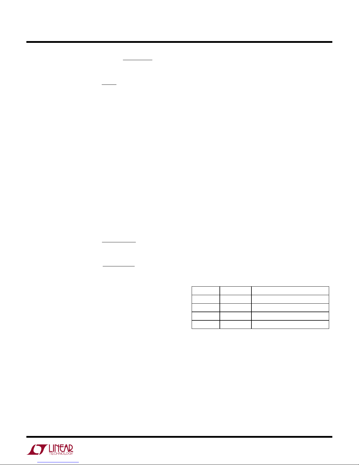
PERFORMANCE SUMMARY
PARAMETER CONDITIONS MIN TYP MAX UNITS
Input Supply Range (V
Absolute Wall Input Threshold (VW) V
DV
Operating Voltage 1.6 5.5
CC
DVCC UVLO (V
V
Regulated Output Voltage (V
BAT
Constant Current Mode Charge Current (I
V
UVLO V
OUT
V
OUT1
V
OUT2
V
OUT3
LDO1
LDO2
Full-Scale LED Current 20 m
DVCC,UVLO)
BUS
)
) DC1592A-A (LTC3577-3)
FLOAT
CHRG
WALL
V
WALL
1
DC1592A-B (LTC3577-4)
) R
PROG
OUT
V
OUT
0 to 500mA 1.8
0 to 500mA 3.3
0 to 800mA 1.2
0 to 150mA 3.3
0 to 150mA 1.2
Specifications are at TA = 25°C
4.35 5.5
Rising
Falling
= 2KΩ, Input current limit = 1A 465 500 535 m
Falling
Rising
4.3
3.1
3.2
4.179
4.200
4.079
4.100
2.5 2.7
2.8 2.9
4.45
4.221
4.121
1
Page 2

LTC3577-3 AND LTC3577-4
QUICK START PROCEDURE
Demo Circuit 1592 is designed to be used with a USB
input and/or a 5V adaptor input. Demo Circuit 1592 utilizes the DC590B, USB to I2C interface board, to control
the LED boost driver, LDO enables, and buck modes. It is
also used to monitor the buck and LDO outputs, plus
battery charger status. This circuit may be evaluated using a lithium ion battery or a
battery simulator consist-
ing of a 0V-5V, 3A power supply and a 3.6Ω power
resistor.
The DC1592 is easy to set up to evaluate the performance of the LTC3577-3 and LTC3577-4. Refer to
X
Figure 1X
and Figure 2 for proper measurement equipment setup
and follow the procedure below to evaluate using the
DC590B board:
NOTE. When measuring the input or output voltage ripple, care must be
taken to avoid a long ground lead on the oscilloscope probe. Measure the
input or output voltage ripple by touching the probe tip directly across
X
the VUSB, WALL, or VOUT and GND terminals. See
scope probe technique.
Figure 2X for proper
1. Refer to the DC590B Quick Start Guide for QuikEvalTM
setup and software installation details.
2. Set the VCCIO jumper, JP6, on the DC590B board to
the 3.3V position.
NOTE. The DVCC voltage level may be selected on the DC590B. This is
done by setting the VCCIO jumper, JP6, on the DC590B board to one of
the following settings: 3.3V, 5V, removed for 2.7V or set to external if an
external supply is desired to be used.
3. Make sure the USB cable is connected between the
computer and the DC590B controller board.
4. Set the jumpers on the DC1592 board to the following
settings:
JP1.
ILIM0 to “0” position.
JP2.
ILIM1 to “0” position.
JP3.
NTC to “INT” position.
JP4.
PWR_ON CNTL to “SW” position.
6. With power off, connect a 5V, 1A power supply to
VUSB and GND with a series ammeter and a voltmeter
as shown in
X
Figure 1X.
7. Connect a battery or a battery simulator set to 3.6V
between BAT and GND with a series ammeter and a
voltmeter as shown in
Turn on and set the VUSB input power supply to 5V.
8.
X
Figure 1X.
The DC590B board gets its power from the USB cable.
Run the QuikEval.exe program. The LTC3577-
9.
3/LTC3577-4 control window (shown in
pops up.
NOTE. The Status indicators on the software control window may display
“N/A” when an I2C ACK was not received. This occurs when the part is in
the power down (PDN) state or when DVCC is missing. Please refer to
the LTC3577 datasheet for more information on the PDN state.
X
Figure 3X)
10. On the LTC3577-3/LTC3577-4 control window, se-
lect the PWR_ON HI/LOW button. When “HI” is indicated on the button, the PWR_ON pin goes high and
the LDO2, VOUT1, and VOUT2 outputs sequence up.
VOUT POWER GOOD for each output is indicated on
the STATUS section on the control window.
11. On the LTC3577-3/LTC3577-4 control window, se-
lect the EN3 HI/LOW button. When “HI” is indicated
on the button, the EN3 pin goes high and the VOUT3
powers up. VOUT POWER GOOD for VOUT3 is indicated on the STATUS section on the control window.
12. On the LTC3577-3/LTC3577-4 control window, se-
lect the BUCK1 through BUCK3 MODE buttons to
switch the bucks into Burst mode. Observe the output
ripple and the quiescent current before and after
switching modes.
13. Select the desired BUCK SW SLEW RATE option but-
ton to switch between a fast rise-time for best efficiency to a slower rise time with better EMI performance.
JP5.
VINLDO2 to “VOUT” position.
5. Connect DC1592 to the DC590B USB Serial Controller
using the supplied 14-conductor ribbon cable as
shown in
X
Figure 1X.
2
14. Set the LED DAC REG vertical slider to a desired cur-
rent level. The LED current and the LED DAC register
setting are displayed in the test boxes below the vertical slider. The LED full scale current (I
LED(FS)
) for this
circuit is 20mA.
Page 3
R
N
N
LTC3577-3 AND LTC3577-4
15. Select the LED EN/DIS button to turn on the LEDs.
Select the button again to turn off the LEDs.
16. Select the “460ms” GRADATION TIME option button
then select the LED EN/DIS button. Observe how the
LEDs turn on and off smoothly when the LED boost
circuit is enabled and disabled.
17. Select the “PWM” LED MODE option button. This
allows the LED intensity to be adjusted with the PWM
controls as well as the DAC register.
18. Set the “PWM Numerator” and the “PWM Denomi-
nator” vertical sliders to their maximum position. The
hexadecimal value of “F” is displayed in the setting
text boxes below the sliders. The PWM duty cycle and
frequency are also displayed below the setting text
boxes.
19. With the LED boost enabled, reduce the “PWM Nu-
merator” vertical slider while observing the LED intensity. Notice that the LEDs dim as the numerator is decreased.
20. Select a different “PWM Clock Speed” option button
and observe the PWM frequency changes accordingly.
21. Set the WALL input, PS1, to 5V. Observe that the
input current is now coming from the WALL input instead of the VUSB input and VOUT.
22. Refer to the “USING THE LTC3577-3/LTC3577-4
SOFTWARE” section for more information on how to
II
I
Frequency =
)(
FSLEDLED
)(
FSLED
CycleDuty =
⎛
••=
3^10
⎜
⎝
V
8.0
500
•=
18
PWMNUM
PWMDE
PWMCLK
PWMDE
DAC
63
−
63
⎞
⎟
⎠
control the device using the LTC3577-3/LTC3577-4
control window.
23. Set the “PWR_ON CNTL” jumper, JP4, to the “PB”
position to power up/down the device with the “ON”
pushbutton, PB1.
24. Depress the “ON” pushbutton, PB1 (minimum of
400ms). LDO2, VOUT1, and VOUT2 outputs sequence
up. If EN3 HI/LOW button is in the “HI” position,
VOUT3 will also power up. VOUT POWER GOOD for
each output is indicated on the STATUS section on the
control window.
25. Wait at least five seconds from depressing PB1, then
depress the “PWR_ON” pushbutton, PB2. LDO2,
VOUT1, and VOUT2 (VOUT3 if powered up) outputs
shutdown.
26. Again depress PB1, the “ON” pushbutton. LOD2,
VOUT1, and VOUT2 outputs sequence up.
27. Wait at least five seconds from depressing PB1, and
then depress and hold PB1 for at least 14 seconds.
PGOOD will transition low for 1.8ms to allow the microprocessor to reset.
28. The input current limit may be adjusted by changing
the “ILIM0” and “ILIM1” jumpers, JP1 and JP2 respectively. See Table 1 for details.
Table 1. Input Current Limit Settings
ILIM1 ILIM0 CURRENT LIMIT
0 0 100mA (1X)
0 1 1A (10X)
1 0 0.5mA (SUSP)
1 1 500mA (5X)
29. Refer to the LTC3577-3 and LTC3577-4 datasheet
for more details on how the LTC3577 operates.
30. When done, turn off all loads and power supplies
and then close the LTC3577-3/LTC3577-4 control window.
3
Page 4

LTC3577-3 AND LTC3577-4
Proper Measurement Equipment Setup
VIN
GND
Figure 1. Measuring Input or Output Ripple
USING THE LTC3577-3/LTC3577-4 SOFTWARE
The LTC3577-3/LTC3577-4 program provides control of
the mode and slew rate of the buck regulators. It also
controls the intensity and slew rate of the LED boost controller and allows the user to view the contents of the
status register.
VIEW LTC3577 PRODUCT PAGE
net browser and searches the Linear Technology Corporation web site for information on the LTC3577 when an
internet connection is available.
button opens an inter-
4
Page 5

REG0
through
decimal value that has been written to the corresponding
registers of the LTC3577-3/LTC3577-4.
STATUS REG
value that has been last read from the LTC35773/LTC3577-4 status register.
BUCK1
individually set each buck regulator into Pulse Skip Mode
or Burst Mode for light loads.
BUCK SW SLEW RATE
choose one of four slew rates for optimal EMI reduction
or efficiency.
PWR_ON HI/LOW
PWR_ON pin high or low to turn on or off LDO2, VOUT1,
and VOUT2.
EN3 HI/LOW
or low to turn on or off VOUT3.
AUTO READ BACK ENABLED/DISABLED
used to automatically update the status register every
250ms when enabled. When disabled the read register
may be updated by selecting the “Read Back Status” button.
Read Back Status
register when selected.
AUTO UPDATE ENABLED/DISABLED
used to automatically update the LTC3577-3/LTC3577-4
I
sliders have been changed. When disabled the LTC35773/LTC3577-4 I
the “Update All Registers” button.
Update All Registers
LTC3577-3/LTC3577-4 I2C write registers when selected.
LED EN/DIS
LED boost controller.
BOOST SW SLEW RATE FAST/SLOW
turn on and off the LED switch faster or slower for optimal efficiency or EMI reduction.
through
2
C registers when any of the Buck or LED buttons or
REG3
text box windows display the hexa-
text box window displays the hexadecimal
BUCK3 MODE
select button is used to set the
select button is used to set the EN3 pin high
button is used to update the status
2
C registers may be updated by selecting
button is used to update all of the
select button is used to enable or disable the
select buttons are used to
option buttons are used to
select button is
select button is
button is used to
LTC3577-3 AND LTC3577-4
LED MODE
three Boost controller modes. CC Boost mode is a constant current mode that allows the LED current to be
controlled by the LED DAC REG vertical slider. HV Boost
mode regulates the ILED pin to 0.8V to operate the Boost
at a fixed voltage. HV Boost mode should not be enabled
unless the demo circuit has been modified to support
this mode of operation. PWM mode allows the LED in-
tensity to be controlled by pulse width modulating the
LEDs based on the LED DAC REG, PWM Numerator,
PWM Denominator, and PWM Clock Speed settings.
NOTE:
are disabled.
GRADATION TIME
gradate up to or down from the selected LED intensity
whenever the LED controller is enabled or disabled.
LED DAC REG
from 20uA to 20mA in 64 logarithmic steps. The LED
intensity slider may be adjusted by clicking on the up or
down arrows to increment or decrement by one LSB or
by clicking and dragging the slide pointer. The hex code
and LED current is displayed in the two text boxes below
the slider.
PWM Clock Speed
PWM clock speed. The PWM clock speed is divided by
the PWM denominator to determine the PWM frequency.
PWM Numerator
numerator value. The PWM numerator is divided by the
PWM denominator to determine the PWM duty cycle.
PWM Denominator
denominator value. The PWM denominator is used in
conjunction with the PWM numerator to determine the
PWM duty cycle and with the PWM clock speed to determine the PWM frequency.
STATUS
status determined by the LTC3577-3/LTC3577-4 status
register.
option buttons are used to choose one of
When in CC Boost or HV Boost LED modes, the PWM controls
option buttons set the desired time to
vertical slider controls the LED current
option buttons are used to select the
vertical slider is used to select a PWM
vertical slider is used select a PWM
indicators display the charge, NTC, and power
5
Page 6

LTC3577-3 AND LTC3577-4
Figure 2. LTC3577-3/LTC3577-4 Software Control Window
6
Page 7

LTC3577-3 AND LTC3577-4
7
Page 8

LTC3577-3 AND LTC3577-4
8
Page 9

Mouser Electronics
Authorized Distributor
Click to View Pricing, Inventory, Delivery & Lifecycle Information:
Analog Devices Inc.:
DC1592A-A DC1592A-B
 Loading...