

Page 1
Description
DEMO MANUAL DC2565A
LT8607
42V, 0.75A Micropower Synchronous
Step-Down Regulator
Demonstration Circuit 2565A is a 42V, 0.75A micropower
synchronous step-down regulator featuring the LT®8607.
The demo board is designed for 5V output from a 5.5V
to 42V input. The wide input range allows a variety of
input sources, such as automotive batteries and industrial supplies. The LT8607
is a compact, high efficiency,
high speed synchronous monolithic step-down switching regulator that consumes less than 3μA of quiescent
current when output is regulated at 5V. Top and bottom
power switches, compensation components and other
necessary circuits are inside of the LT8607 to minimize
external components and simplify design.
The SYNC pin on the demo board is grounded by default
for low ripple Burst Mode® operation. Move JP1 to PULSE
SKIPPING position can change the operation mode to
pulse-skipping operation. Once JP1 is on SPREAD SPECTRUM position, VCC is applied to the SYNC pin for low
EMI spread spectrum operation. To synchronous to an
external clock, move JP1 to SYNC and apply the external
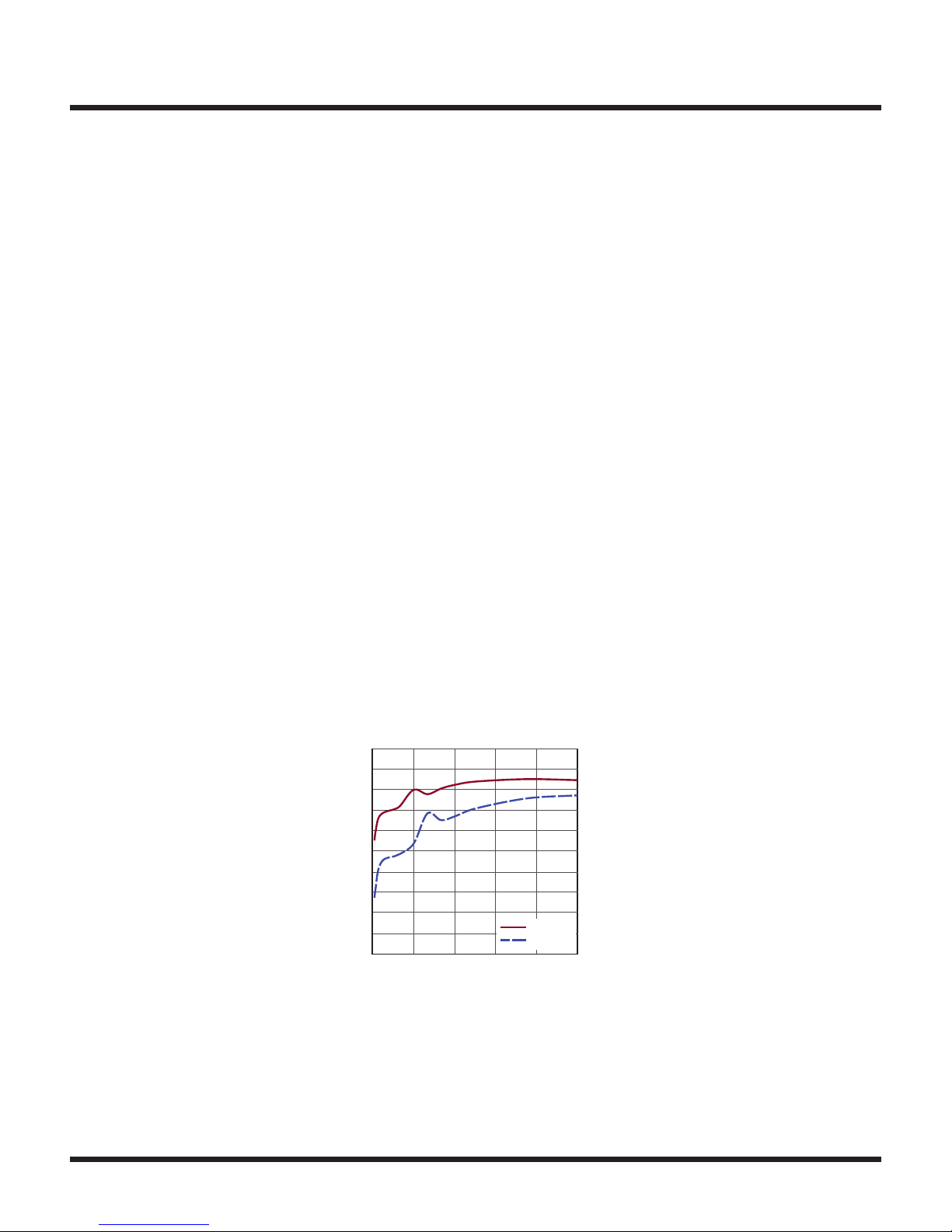
clock to the SYNC turret. Figure 1 shows the efficiency
of the circuit.
The demo board has an EMI filter installed. The radiated
EMI performances of the board (with EMI filter) are shown
in Figure 2 and Figure 3. The red lines in Figure 2 and
Figure 3 are CISPR25 Class 5 peak limit. To use the EMI
filter, the input should be tied to V
, not VIN. An induc-
EMI
tor L2, which is a 0Ω jumper on the board by default
now, can be added in the EMI filter to further reduce the
conducted emission.
The LT8607 data sheet gives a complete description of
the part, operation and application information. The data
sheet must be read in conjunction with this demo manual
for DC2565A.
Design files for this circuit board are available at
http://www.linear.com/demo/DC2565A
L, LT, LTC, LTM, Linear Technology, the Linear logo and Burst Mode are registered trademarks
of Analog Devices, Inc. All other trademarks are the property of their respective owners.
performance summary
SYMBOL PARAMETER CONDITIONS MIN TYP MAX UNITS
V
IN
V
OUT
I
OUT
f
SW
EFE Efficiency at DC V
Input Voltage Range 5.5 42 V
Output Voltage 4.8 5 5.2 V
Maximum Output Current 0.75 A
Switching Frequency 1.85 2 2.15 MHz
Specifications are at TA = 25°C
= 12V, I
IN
= 0.75A 92.4 %
OUT
dc2565af
1
Page 2
DEMO MANUAL DC2565A
DC2565A F01
Quick start proceDure
DC2565A is easy to set up to evaluate the performance
of the LT8607. Refer to Figure 4 for proper measurement
equipment setup and follow the procedure below:
NOTE: When measuring the input or output voltage ripple,
care must be taken to avoid a long ground lead on the
oscilloscope probe. See Figure 5 for the proper scope
technique.
1. Set an input power supply that is capable of 42V/0.75A.
Then turn off the supply.
2. With power off, connect the supply to the input termi-
nals V
and GND.
IN
3. Turn on the power at the input.
NOTE: Make sure that the input voltage never exceeds
42V.
4. Check for the proper output voltage of 5V. Turn off the
power at the input.
5. Once the proper output voltage is established, connect
a variable load capable of sinking 0.75A at 5V to the
output terminals V
and GND. Set the current for 0A.
OUT
a. If efficiency measurements are desired, an ammeter
can be put in series with the output load in order to
measure the DC2565A’s output current.
b. A voltmeter can be placed across the output ter-
minals in order to get an accurate output voltage
measurement.
6. Turn on the power at the input.
NOTE: If there is no output, temporarily disconnect the
load to make sure that the load is not set too high.
7. Once the proper output voltage is established again,
adjust the load and/or input within the operating range
and observe the output voltage regulation, ripple voltage, efficiency and other desired parameters.
8. An external clock can be added to the SYNC terminal when SYNC function is used (JP1 on the SYNC
position). Please ensure that the chosen RT sets the
LT8607 switching frequency to equal or below the lowest SYNC frequency. See the Synchronization section
in the data sheet.
Figure 1. Efficiency vs Load Current at 2MHz Switching Frequency
2
100
95
90
85
80
75
70
EFFICIENCY
65
60
55
50
0
0.3 0.45 0.6 0.75
0.15
I
OUT
(A)
VIN = 12V
= 24V
V
IN
dc2565af
Page 3

Quick start proceDure
DEMO MANUAL DC2565A
50
VERTICAL POLARIZATION
45
PEAK DETECTOR
40
35
30
25
20
15
10
AMPLITUDE (dBuV/m)
–10
5
0
–5
100 200 300 400 500 600 700 800 900 1000
0
FREQUENCY (MHz)
CLASS 5 PEAK LIMIT
FIXED FREQUENCY
SPREAD SPECTRUM MODE
DC2565A F02
Figure 2. LT8607 Demo Circuit EMI Performance in CISPR25
Radiated Emission Test, Antenna Polarization: Vertical
(VIN = 14V, V
OUT
= 5V, I
= 0.75A, 2MHz Switching Frequency)
OUT
50
HORIZONTAL POLARIZATION
45
PEAK DETECTOR
40
35
30
25
20
15
10
AMPLITUDE (dBuV/m)
–10
5
0
–5
100 200 300 400 500 600 700 800 900 1000
0
FREQUENCY (MHz)
CLASS 5 PEAK LIMIT
FIXED FREQUENCY
SPREAD SPECTRUM MODE
DC2565A F03
Figure 3. LT8607 Demo Circuit EMI Performance in CISPR25
Radiated Emission Test, Antenna Polarization: Horizontal
(VIN = 14V, V
OUT
= 5V, I
= 0.75A, 2MHz Switching Frequency)
OUT
Figure 4. Proper Measurement Equipment Setup
V
OUT
GND
Figure 5. Measuring Output Ripple
dc2565af
3
Page 4

DEMO MANUAL DC2565A
parts List
ITEM QTY REFERENCE PART DESCRIPTION MANUFACTURER/PART NUMBER
Required Circuit Components
1 1 C2 CAP., X7R, 4.7µF, 50V, 10% 1206 MURATA, GRM31CR71H475K
2 1 C4 CAP., X7R, 0.22µF, 16V, 10%, 0603 MURATA, GRM188R71C224KA01D
3 1 C5 CAP., C0G, 10pF, 25V, 5%, 0603 AVX, 06033A100JAT2A
4 1 C6 CAP., X7R, 22µF, 10V, 10%, 1206 MURATA, GRM31CR71A226KE15L
5 1 C7 CAP., X7R, 1.0µF, 25V, 10%, 0603 MURATA, GRM188R71E105KA12D
6 1 C8 CAP., X7R, 0.01µF, 16V, 10%, 0603 MURATA, GRM188R71C103KA01D
7 1 L1 IND., 3.3µH WURTH ELECTRONICS, 74438336033
8 1 R2 RES., CHIP, 18.2k, 1/10W, 1%, 0603 VISHAY, CRCW060318K2FKEA
9 1 R3 RES., CHIP, 49.9k, 1/10W, 1%, 0603 VISHAY, CRCW060349K9FKEA
10 2 R1, R4 RES., CHIP, 1M, 1/10W, 1%, 0603 VISHAY, CRCW06031M00FKEA
11 1 R5 RES., CHIP, 187k, 1/10W, 1%, 0603 VISHAY, CRCW0603187KFKEA
12 1 U1 IC, REGULATOR, MSE10 LINEAR TECH., LT8607EMSE#PBF
Additional Demo Board Circuit Components
1 1 C1 CAP., ALUM 22µF 63V SUN ELECT, 63CE22BS
2 2 C3, C10 CAP., X7R, 4.7µF, 50V, 10% 1206 MURATA, GRM31CR71H475K
3 1 C9 CAP., X7R, 4.7µF, 16V, 10%, 0805 MURATA, GRM21BR71C475K73L
4 1 C11 CAP., X7R, 1µF, 50V, 10%, 0805 MURATA, GRM21BR71H105KA12L
5 2 C12, C13 CAP., X7R, 0.1µF, 50V, 10%, 0603 MURATA, GRM188R71H104KA93D
6 1 FB1 FERRITE BEAD 0805 TDK, MPZ2012S331AT000
7 1 L2 RES., CHIP, 0Ω, 3/4W, 2010 VISHAY, CRCW20100000Z0EF
8 0 R6 (OPT.) RES., 0603
Hardware: For Demo Board Only
1 9 E1-E9 TESTPOINT, TURRET, 0.094" MILL-MAX, 2501-2-00-80-00-00-07-0
2 1 E10 (OPT.) TESTPOINT, TURRET, 0.094"
3 1 JP1 DOUBLE ROW HEADER 2 × 4 0.079" WURTH ELECTRONICS, 62000821121
4 1 XJP1 SHUNT, 0.079" CENTER WURTH ELECTRONICS, 60800213421
5 4 MH1-MH4 STAND-OFF, NYLON 0.50" TALL WURTH ELECTRONICS, 702935000
4
dc2565af
Page 5

schematic Diagram
D
VOUT
5V /0.75A
GND
DEMO MANUAL DC2565A
PG
E3
C4
L1
0.22µF
VOUT
3.3µH
2
10
C9
C6
74438336033
SW
EN/UV
1
2
1
BST
U1
LT8607EMSE
3
VIN
9
4.7µF
22µF
SYNC
5
16V
10V
R3
0805
1206
8
3
PG
VCC
E4
R4
49.9k
6
7
FB
TR/SS
1.00M
4
E8
1
C5
10pF
R5
187k
GND
11
RT
2
3
R2
18.2k
R6
(Opt)
R1
1.00M
C13
0.1µF
50V
C2
4.7µF
50V
1206
SUNCON
63CE22BS
C1
22µF
4
5
E10
VIN
5.5V - 42V
D
63V
+
0 2010
L2
C10
4.7µF
FB1
C3
4.7µF
MPZ2012S331AT000
C12
0.1µF
C11
1µF
E1
VEMI
5.5V - 42V
50V
50V
50V
50V
GND
1206
1206
0805
E2
E6
EN/UV
C C
VCC
E5
SYNC
JP1
C7
1 2
VCC
1µF
SYNC
(2MHz)
SPREAD SPECTRUM
PULSE SKIPPING
BURST
4
6
8
357
E7
TR/SS
C8
0.01µF
4
E9
GND
B B
ALL CAPACITORS ARE 0603.
NOTES: UNLESS OTHERWISE SPECIFIED
1. ALL RESISTORS ARE 0603.
5
A A
dc2565af
Information furnished by Linear Technology Corporation is believed to be accurate and reliable.
However, no responsibility is assumed for its use. Linear Technology Corporation makes no representation that the interconnection of its circuits as described herein will not infringe on existing patent rights.
5
Page 6

DEMO MANUAL DC2565A
DEMONSTRATION BOARD IMPORTANT NOTICE
Linear Technology Corporation (LTC) provides the enclosed product(s) under the following AS IS conditions:
This demonstration board (DEMO BOARD) kit being sold or provided by Linear Technology is intended for use for ENGINEERING DEVELOPMENT
OR EVALUATION PURPOSES ONLY and is not provided by LTC for commercial use. As such, the DEMO BOARD herein may not be complete
in terms of required design-, marketing-, and/or manufacturing-related protective considerations, including but not limited to product safety
measures typically found in finished commercial goods. As a prototype, this product does not fall within the scope of the European Union
directive on electromagnetic compatibility and therefore may or may not meet the technical requirements of the directive, or other regulations.
If this evaluation kit does not meet the specifications recited in the DEMO BOARD manual the kit may be returned within 30 days from the date
of delivery for a full refund. THE FOREGOING WARRANTY IS THE EXCLUSIVE WARRANTY MADE BY THE SELLER TO BUYER AND IS IN LIEU
OF ALL OTHER WARRANTIES, EXPRESSED, IMPLIED, OR STATUTORY, INCLUDING ANY WARRANTY OF MERCHANTABILITY OR FITNESS
FOR ANY PARTICULAR PURPOSE. EXCEPT TO THE EXTENT OF THIS INDEMNITY, NEITHER PARTY SHALL BE LIABLE TO THE OTHER FOR
ANY INDIRECT, SPECIAL, INCIDENTAL, OR CONSEQUENTIAL DAMAGES.
The user assumes all responsibility and liability for proper and safe handling of the goods. Further, the user releases LTC from all claims
arising from the handling or use of the goods. Due to the open construction of the product, it is the user’s responsibility to take any and all
appropriate precautions with regard to electrostatic discharge. Also be aware that the products herein may not be regulatory compliant or
agency certified (FCC, UL, CE, etc.).
No License is granted under any patent right or other intellectual property whatsoever. LTC assumes no liability for applications assistance,
customer product design, software performance, or infringement of patents or any other intellectual property rights of any kind.
LTC currently services a variety of customers for products around the world, and therefore this transaction is not exclusive.
Please read the DEMO BOARD manual prior to handling the product. Persons handling this product must have electronics training and
observe good laboratory practice standards. Common sense is encouraged.
This notice contains important safety information about temperatures and voltages. For further safety concerns, please contact a LTC application
engineer.
Mailing Address:
Linear Technology
1630 McCarthy Blvd.
Milpitas, CA 95035
Copyright © 2004, Linear Technology Corporation
6
dc2565af
LT 0517 • PRINTED IN USA
LINEAR TECHNOLOGY CORPORATION 2017
 Loading...