

Page 1

DESCRIPTIO
DEMO MANUAL DC239
NO-DESIGN SWITCHER
LTC1502-3.3
Single Cell to 3.3V Regulated
Charge Pump DC/DC Converter
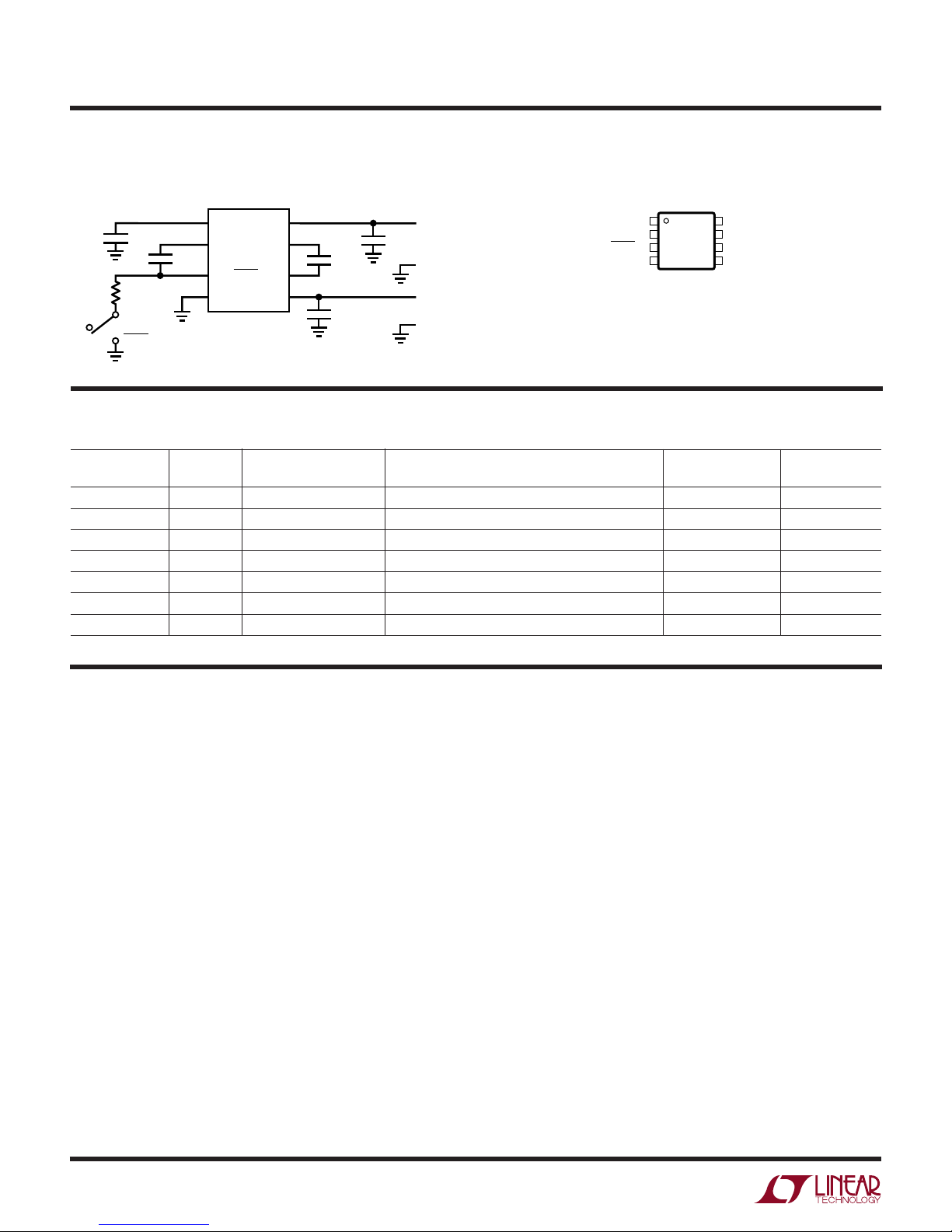
U
Demonstration Circuit DC239 is a quadrupler charge pump
DC/DC converter that produces a regulated 3.3V output
from a single alkaline cell input. The circuit requires only
five small external capacitors and no inductors. Low
supply current (40µA typ) and minimal external compo-
nent area make this power supply ideal for space and
power conscious single-cell applications. The maximum
output load is 10mA for input voltages greater than or
equal to 1V. A jumper is available to put the circuit into
shutdown mode, which reduces input quiescent current to
5µA (typ) and disconnects V
from VIN. Gerber files for
OUT
this circuit are available. Call the LTC factory.
, LTC and LT are registered trademarks of Linear Technology Corporation.
UWWW
PERFOR A CE SU ARY
PARAMETER CONDITIONS MIN TYP MAX UNITS
VIN Operating Voltage 0.9 1.8 V
Minimum V
V
OUT
VIN Operating Current I
VIN Shutdown Current C1
Output Ripple I
Efficiency VIN = 1V, I
Start-Up Voltage 100kΩ V
IN
Operating Temperature Range 0°C to 70°C
Load 0.75 0.9 V
OUT
I
≤ 10mA, 1V ≤ VIN ≤ 1.8V 3.17 3.3 3.43 V
OUT
= 0mA, 0.9V ≤ VIN ≤ 1.8V 40 90 µA
OUT
–
/SHDN = 0V, 0.9V ≤ VIN ≤ 1.8V 5 15 µA
= 10mA, VIN = 1.25V 50 mV
OUT
= 10mA 77 %
OUT
P-P
U
W
TYPICAL PERFOR A CE CHARACTERISTICS A D BOARD PHOTO
Output Voltage vs Input Voltage
3.5
T
= 25°C
A
3.4
I
= 1mA
3.3
3.2
OUTPUT VOLTAGE (V)
3.1
3.0
0.8
OUT
I
= 10mA
OUT
= 15mA
I
OUT
1.0
1.2
INPUT VOLTAGE (V)
1.4
1.6
1502-3.3 TA02
U
Component Side
1.8
1
Page 2
DEMO MANUAL DC239
1
2
3
4
C2
C1
+
C1–/SHDN
GND
8
7
6
5
V
OUT
C3
+
C3
–
V
IN
TOP VIEW
MS8 PACKAGE
8-LEAD PLASTIC MSOP
NO-DESIGN SWITCHER
W
U
W
SCHE ATIC A D PACKAGE DIAGRA S
Demo Board Schematic
ON
C2
10µF
R1
100Ω
JP1
SHDN
C1
1µF
1
C2
2
C1
LTC1502-3.3
3
C1–/SHDN
4
GND
U1
8
V
OUT
+
7
+
C3
–
C3
V
IN
C3
1µF
6
5
C
IN
10µF
C
OUT
10µF
DC239 SCHEM
J2
V
OUT
3.3V/10mA
J1
J3
V
IN
J4
LTC1502CMS8-3.3
PARTS LIST
REFERENCE
DESIGNATOR QUANTITY PART NUMBER DESCRIPTION VENDOR TELEPHONE
C1, C3 2 0603ZG105ZAT1A 1µF 10V Y5V Capacitor AVX (843) 946-0362
C2, C
JP1 1 2802S-03G2 3-Pin, 2mm Jumper Comm Con (626) 301-4200
J1, J2, J3, J4 4 2501-2 0.090 Turret Testpoint Mill-Max (516) 922-6000
R1 1 CR16-101JM 100Ω 1/16W 5% Chip Resistor TAD (800) 508-1521
U1 1 LTC1502CMS8-3.3 MSOP Step-Up DC/DC IC LTC (408) 432-1900
OUT
, C
IN
3 1206ZG106ZAT1A 10µF 10V Y5V Capacitor AVX (843) 946-0362
1 CCIJ2mm-138-G 2-Pin 2mm Shunt Comm Con (626) 301-4200
U
OPERATIO
The LTC1502-3.3 uses a switched capacitor quadrupler
charge pump to produce a boosted output voltage. The
quadrupler charge pump consists of two voltage doubler
charge pumps (CP1 and CP2 on the Block Diagram)
cascaded in series. CP1 doubles the input voltage VIN, and
the CP1 output voltage is stored on external capacitor C2.
The C2 pin also serves as the input for doubler CP2, whose
output is stored on the output capacitor C
doubler is controlled by a 2-phase clock that is generated
in the timing-control circuit. On phase one of the clock, the
flying capacitors C1 and C3 are charged to their respective
input voltages. On phase two, each charged flying capacitor is stacked on top of the input voltage and discharged
through an internal switch onto its respective output. This
sequence of charging and discharging the flying capacitors (CP1 and CP2) continues at the free running oscillator
frequency (500kHz typ) until the output is in regulation.
Regulation is achieved by comparing the divided output
voltage to a fixed voltage reference. The charge pump
2
OUT
. Each
clocks are disabled when the output voltage is above the
desired regulation point set by COMP1. When the output
has dropped below the lower trip point of COMP1, the
charge pump clocks are turned back on until V
OUT
is
boosted back into regulation.
Enhanced Start-Up
Enhanced start-up capability is provided by the COMP2
circuitry. COMP2 compares the divided C2 voltage to the
input voltage, VIN. The COMP2 output disables the output
charge pump, CP2, whenever the divided C2 voltage is
lower than VIN. The CP2 output is thereby forced into a
high impedance state until the voltage on C2 has been
raised above VIN (the C2 pin should not be loaded for
proper start-up). This allows a higher internal gate drive
voltage to be generated (from the C2 pin) before the part’s
output (V
forces CP2 to be turned ON and OFF while C
) is connected to a load. Hysteresis in COMP2
OUT
is charged
OUT
Page 3

OPERATIO
DEMO MANUAL DC239
NO-DESIGN SWITCHER
U
LTC1502-3.3 Block Diagram
C2
SHUTDOWN
–
/SHDN
C1
V
IN
5
C
IN
U2
2.5µA
–
+
+
0.55V
SHDN OSCEN
HIZ1
CLK1/CLK2
TIMING
CONTROL
32
CP1
+
C1
400k
V
IN
C2
1 6 7
–
+
1M
U3
COMP2COMP3
U4
C3
HIZ2
C3C1
–
CP2
+
C3
8
2.1M
V
OUT
C
OUT
–
1.2M
+
C2
V
OUT
BIAS
CONTROL
INTERNAL
V
CC
COMP1
1.2V
REF
4
GND
1502-3.3 BD
to prevent a lock-up condition if C2 droops too low during
start-up. By the time the output nears the regulation point,
the C2 voltage is well above the lower trip point of COMP2
and CP2 will remain enabled. This method of disabling the
output charge pump while an internal boosted gate drive
supply is developed allows the part to start up at low
voltages with a larger output current load than would
otherwise be possible.
Shutdown
Shutdown is implemented using an external pull-down
device on the C1–/SHDN pin. The demo circuit provides a
jumper that selects either the ON or SHDN state. In the ON
state, the 100Ω external pull-down resistor is left floating.
In the SHDN state, the resistor is shorted to ground
through the jumper. The center pin of the jumper can be
driven with an external, open-drain device to test the AC
start-up and shutdown characteristics. The shutdown
feature can be used to prevent charge pump switching
during noise sensitive intervals. The LTC1502-3.3 takes
between 20µs and 50µs to switch from shutdown to active
mode once the pull-down device has been turned off.
During shutdown, V
is disconnected from VIN.
OUT
Short-Circuit Protection
When the output pin is shorted to ground, the LTC1502-
3.3 will continuously charge the C2 capacitor to approximately 1.4 times VIN and then discharge C2 into the
shorted output. Since the discharging of C2 into V
OUT
will
bring the C2 voltage below the COMP2 start-up trip
voltage, the output charge pump will be forced Hi-Z while
C2 charges again. Hence, the internal charge pump gate
drive voltage is limited to 1.4 • V
IN(MAX)
and no continuous current is supplied to V
(on the C2 pin),
. The result-
OUT
ing output short-circuit current is limited to under 30mA
(typ), thereby allowing the LTC1502-3.3 to endure an
indefinite output short circuit without damage. When the
short is removed, the part will start up and operate
normally.
Information furnished by Linear Technology Corporation is believed to be accurate and reliable.
However, no responsibility is assumed for its use. Linear Technology Corporation makes no representation that the interconnection of its circuits as described herein will not infringe on existing patent rights.
3
Page 4

DEMO MANUAL DC239
NO-DESIGN SWITCHER
W
PCB LAYOUT AUD FIL
Component Side Silkscreen Component Side Solder Mask
Component Side Paste Mask
Copper Layer 1 (Top)
Copper Layer 2
Solder Side Solder Mask
U
PC FAB DRAWI
G
A
Linear Technology Corporation
4
1630 McCarthy Blvd., Milpitas, CA 95035-7417
(408) 432-1900 ● FAX: (408) 434-0507
●
www.linear-tech.com
2.00
B
B
DC239 FAB DWG
NOTES: UNLESS OTHERWISE SPECIFIED
1. ALL DIMENSIONS ARE IN INCHES
2. FINISHED MATERIAL IS FR4, 0.062 THICK
2 OZ COPPER, 2 LAYERS. PLATED HOLE
WALL THICKNESS 0.001 MIN
3. PROCESS: SMOBC
2.00
SYMBOL
A
B
DIAMETER
0.030
0.094
TOTAL HOLES
NUMBER
OF HOLES
PLTD
3
PLTD
4
PLTD
7
dc239f LT/TP 0799 500 • PRINTED IN USA
LINEAR TECHNOLOGY CORPORATION 1999
 Loading...