

Page 1

DESCRIPTION
DEMO MANUAL DC2341A
LTC7130EY
20V 20A Monolithic Buck Converter
with Ultra-Low DCR Sensing
Demonstration circuit 2341A is a high efficiency synchronous buck DC/DC converter with 4.5V to 20V input
range. It can supply 20A maximum load current at 1.5V
®
output. The demo board features the LT C
7130 regulator.
No external MOSFETs are required. It employs an LTC
proprietary current sensing, current mode architecture,
allowing the use of a very low DC resistance (DCR) power
inductor to maximize efficiency in high current applica
tions. Differential output voltage sensing along with a
precision internal reference combine to offer accurate
output regulation. The LTC7130 is housed in a 6.25mm
or forced continuous mode (CCM) operation. The converter
can also be externally synchronized through the MODE/
PLLIN pin (MODE/PLLIN terminal on the board; JP2: no
jumper or BURST position). To shut down the converter,
one simple way is to force the RUN pin below 1.1V (JP1:
OFF). The power good output (PGOOD terminal) is low
when the output voltage is outside of the ±10% regula
-
tion window.
The LTC7130 data sheet gives a complete description of
the operation and application information. The data sheet
must be read in conjunction with this demo manual.
× 7.5mm × 2.22mm 63-pin BGA package.
Design files for this circuit board are available at
The light load operation mode of the converter is deter
mined with the MODE/PLLIN pin. Use the JP2 jumper to
®
select pulse-skipping mode (P.S.), Burst Mode
PERFORMANCE SUMMARY
PARAMETER CONDITIONS MIN TYP MAX UNITS
Input Voltage Range 4.5 20 V
Output Voltage V
Maximum Output Current V
Typical Switching Frequency 530 kHz
Typical Efficiency V
Typical Output Voltage Ripple V
(BURST)
Specifications are at TA = 25°C
-
= 4.5V to 20V, I
IN
= 4.5V to 20V, V
IN
= 12V, I
IN
IN
= 12V, I
OUT
OUT
http://www.linear.com/demo/DC2341A
L, LT, LTC, LTM, Linear Technology, the Linear logo and Burst Mode are registered trademarks
of Linear Technology Corporation. All other trademarks are the property of their respective
owners.
= 0A to 20A 1.5 ±2% V
OUT
= 1.5V 20 A
OUT
= 20A 89.2 %
= 20A 25 mV
P-P
-
dc2341af
1
Page 2
DEMO MANUAL DC2341A
QUICK START PROCEDURE
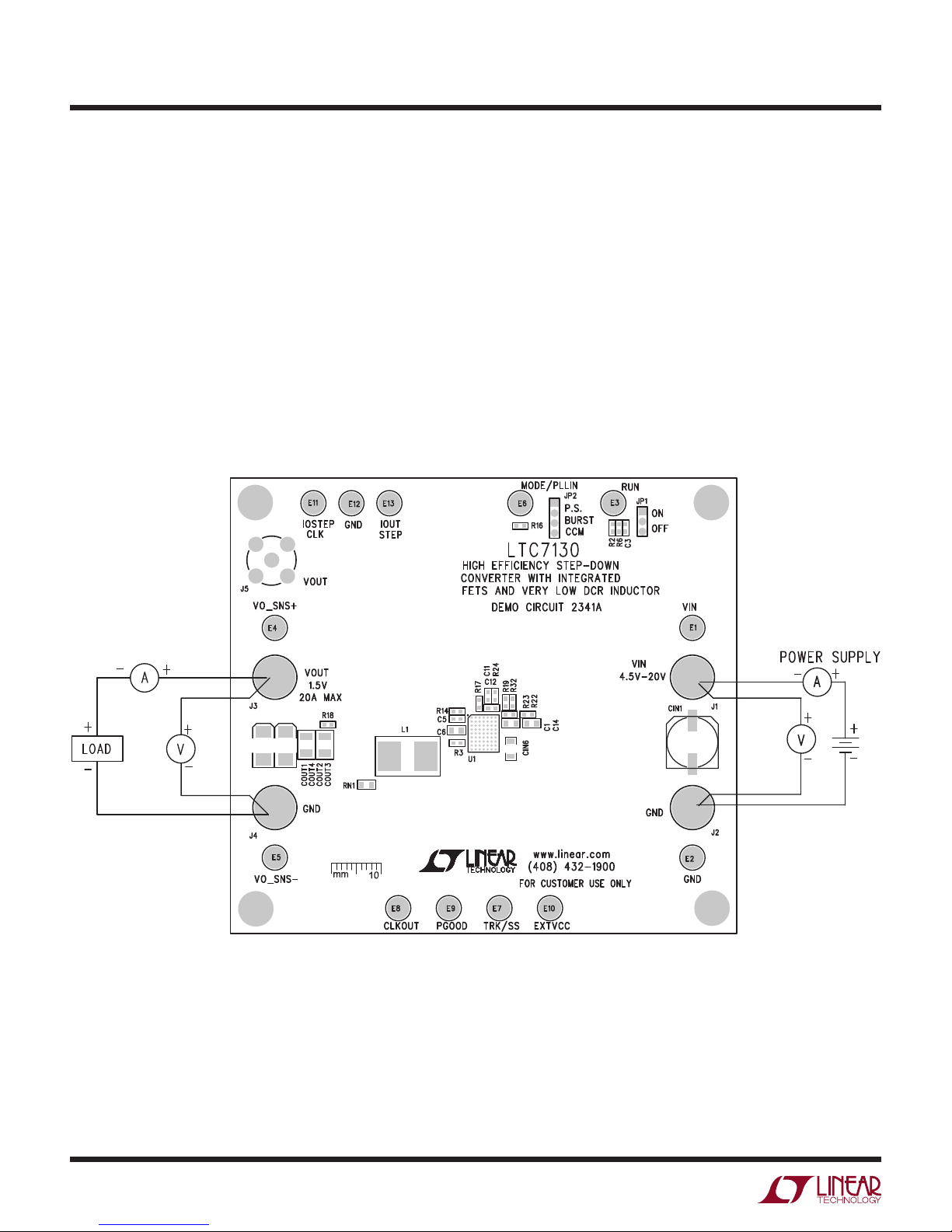
Demonstration circuit 2341A is easy to set up to evaluate
the performance of the LTC7130. Refer to Figure 1 for
the proper measurement equipment setup and follow the
procedure below:
1. With power off, connect the input power supply to V
(4.5V to 20V) and GND (input return).
2. Connect the 1.5V output load between V
(Initial load: no load).
3. Connect the DVMs to the input and outputs.
4. Turn on the input power supply and check for the proper
output voltages. V
should be 1.5V ±2%.
OUT
and GND
OUT
IN
5. Once the proper output voltages are established, adjust
the loads within the operating range and observe the
output voltage regulation, ripple voltage and other
parameters.
NOTE: When measuring the output or input voltage ripple,
do not use the long ground lead on the oscilloscope probe.
See Figure 2 for the proper scope probe technique. Short,
stiff leads need to be soldered to the (+) and (–) terminals
of an output capacitor. The probe’s ground ring needs to
touch the (–) lead and the probe tip needs to touch the
(+) lead.
2
Figure 1. Proper Measurement Equipment Setup
dc2341af
Page 3

QUICK START PROCEDURE
OUT
EFFICIENCY (%)
100
20
TOTAL I
dc2341a F04
DEMO MANUAL DC2341A
+ –
C
OUT
V
GND
Figure 2. Measuring Output Voltage Ripple
95
90
85
80
75
70
65
60
55
50
0
105 15
LOAD CURRENT (A)
4.5V
12V
IN
20V
IN
dc2341a F03
IN
Figure 3. Efficiency vs Load Current (VO = 1.5V, Burst Mode)
V
O
50mV/DIV
AC-COUPLED
10A LOAD STEP
5A/DIV
: 10A TO/
O
FROM 20A
Figure 4. Load Step Transient Test (VIN = 12V) Figure 5. Thermal Picture (VIN = 12V, IO = 20A. 21°C Ambient,
No Forced Airflow)
dc2341af
3
Page 4

DEMO MANUAL DC2341A
PARTS LIST
ITEM QTY REFERENCE PART DESCRIPTION MANUFACTURER/PART NUMBER
Required Circuit Components
1 1 CIN1 CAP, ALUM ELEC180µF 20% 25V PANASONIC., 25SVPF180M
2 2 CIN4, CIN5 CAP, 1210 22µF 20% 25V X5R AVX, 12103D226MAT2A
3 1 CIN6 CAP, 1206 10µF 20% 25V X5R AVX, 12063D106MAT2A
4 2 COUT1, COUT4 CAP, 7343 330µF 20% 2.5V POSCAP PANASONIC, 2R5TPE330M9
5 4 COUT2, COUT3, C15, C16 CAP, 1210 100µF 20% 6.3V X5R AVX, 12106D107MAT2A
6 2 C1, C17 CAP, 0805 1µF 10% 25V X5R AVX, 08053D105KAT2A
7 2 C2, C5, C7 CAP, 0603 220nF 10% 25V X5R MURATA GRM188R71E224KA88D
8 1 C10 CAP, 0603 0.1µF 10% 10V X5R AVX, 0603ZD104KAT2A
9 1 C11 CAP, 2.2nF X7R 50V 5% 0603 AVX, 06035C222JAT2A
10 1 C12 CAP, 0603 120pF 10% 25V NPO AVX, 06033A121KAT2A
11 2 C6, C14 CAP, 0805 4.7µF 20% 10V X5R AVX, 0805ZD475MAT2A
12 1 D1 DOIDE, SCHOTTKY 30V SOD-323 CENTRAL SEMI., CMDSH-3 TR
13 1 L1 IND, 0.25µH WURTH ELEKTRONIK, 744308025
14 1 Q1 MOSFET, N-CH D-S 40V TO252 VISHAY, SUD50N04-8M8P-4GE3
15 1 R1 RES, 2.2Ω 1/10W 5% 0603 VISHAY, CRCW06032R20JNEA
16 4 R8, R16, R17, R20 RES, 0Ω JUMPER 1/10W 0603 VISHAY, CRCW06030000Z0EA
17 2 R19, R30 RES, 10k 1/10W 5% 0603 VISHAY, CRCW060310K0JNEA
18 1 R28 SENSE RES, 2512 0.01Ω 1% 1W VISHAY, WSL2512R0100FEA
19 1 R10 RES 0603 100k 1% 1/10W VISHAY, CRCW0603100KFKEA
20 1 R13 RES 0603 1k 1% 1/10W VISHAY, CRCW06031K00FKEA
21 1 R4 RES, 0603 619Ω 1% 1/10W VISHAY, CRCW0603619RFKEA
22 2 R9, R12 RES, 0603 10Ω 5% 1/10W VISHAY, CRCW060310R0JNEA
23 1 R24 RES, 0603 6.04k 1% 1/10W VISHAY, CRCW06036K04FKEA
24 2 R3 RES, 0603 2.7Ω 1% 1/10W VISHAY, CRCW06032R7FKEA
25 1 R23 RES, 0603 124k 1% 1/10W VISHAY, CRCW0603124KFKEA
26 1 R11 RES, 0603 3.01k 1% 1/10W VISHAY, CRCW06033K01FKEA
27 1 R5 RES, 0603 3.09k 1% 1/10W VISHAY, CRCW06033K09FKEA
28 1 R32 RES, 0603 6.65k 1% 1/10W VISHAY, CRCW06036K65FKEA
29 1 U1 IC, LTC7130EY#PBF LINEAR TECH., LTC7130EY#PBF
Additional Demo Board Circuit Components
30 0 COUT5, COUT6 OPT CAP, 7343 OPTION
31 0 CIN2, CIN3, (OPT) CAP, OPTION
32 0 C3, C4, C8, C9, C13, (OPT) CAP, 0603 OPTION
33 0 RN1, R2, R6, R7, R14, R15, R18, R22,
R25, R27, R29
Hardware: For Demo Board Only
34 13 E1-E13 TESTPOINT, TURRET, 0.094" PbF MILL-MAX, 2501-2-00-80-00-00-07-0
35 1 JP2 HEADER, 4 PIN 0.079" SINGLE ROW SULLINS, NRPN041PAEN-RC
36 1 JP1
37 4 J1-J4 JACK, BANANA KEYSTONE 575-4
38 1 J5 CONN, BNC, 5 PINS CONNEX, 112404
39 4 MH1, MH2, MH3, MH4 STAND-OFF, NYLON 0.50" tall KEYSTONE, 8833
40 2 JP1, JP2 SHUNT, 0.079" CENTER SAMTEC, 2SN-BK-G
RES, 0603 OPTION
HEADER, 3 PIN 0.079" SINGLE ROW SULLINS, NRPN031PAEN-RC
dc2341af
4
Page 5

DEMO MANUAL DC2341A
5
4
3
2
1
SCHEMATIC DIAGRAM
1
1
1
2
2
2
REV
REV
9-2-15PRODUCTION
9-2-15PRODUCTION
9-2-15PRODUCTION
1.5V
20A MAX
VOUT
1210 1210
25V
25V
J3
VOUT
744308025
DCR=0.37mOHM
SW
CIN6
10uF
25V
1206
R1 2.2
J2
E2
GND
GND
Charlie
Charlie
Charlie
REVISION HISTORY
DESCRIPTION DATEAPPROVEDECO REV
REVISION HISTORY
DESCRIPTION DATEAPPROVEDECO REV
REVISION HISTORY
DESCRIPTION DATEAPPROVEDECO REV
2
2
2
__
__
__
CIN5
22uF
25V
CIN4
22uF
25V
CIN3
OPT
25V
+
VIN
OPT
CIN2
+
CIN1
180uF
E1
J1
VIN
VIN
4.5V - 20V
D D
L1 0.25uH
C2
J3
J2
J1
H3
H2
H1
G3
G2
G1
A7
F3
F2
E3
E2
E1
D4
D3
D2
A1
G7
E7
E6
E5
E4
F7
F6
F5
F4
VIN
COUT4
330uF
+
COUT1
330uF
2.5V
+
6.3V
COUT3
100uF
6.3V
100uF
COUT2
0.22uF
25V
SW
SW
SW
SW
SW
SW
SW
SW
SW
NC2
NC1
VIN
VIN
VIN
VIN
VIN
VIN
VIN
VIN
VIN
C1
1uF
RUN
2.5V
GND
GND
GND
GND
GND
GND
GND
GND
OFFON
7343
12101210
25V
7343
R5
R4
D1
R3
F1
D5
R2
3
1
GND
J4
3.09k
1%
619
1%
INTVCC
CMDSH-3
2.7
BOOST
SVIN
OPT
2
JP1
E3
B6
C1
RUN
RUN
R8
C4
R7
SNSA+
D1
INTVCC
R6
OPT
C3
OPT
R9
R12
0
OPT
OPT
C5
220nF
INTVCC
R11
10
10
B2
C6
SNS-
3.01k
R10
4.7uF
R14
U1
C2
1%
100k
6.3V
R15 OPT
OPT
C7
220nF
B1
LTC7130
ILIM
R131k1%
C C
VO_SNS+
E4
A3
DIFFP
SNSD+
1
VO_SNS-
E5
VOUT
R18
OPT
C8
0
R19
10k
R17
A4
A2
DIFFN
DIFFOUT
PGOODC7MODE/PLLIN
CLKOUT
C6
C3
PGOOD
CLKOUT
2
3
MODE/PLLIN
4
P.S.
CCM
BURST
R16 0
E6
MODE/PLLIN
TEMPERATURE COMPENSATION
OPT
C9
OPT
R32
1%
6.65k
1%
A6
VFB
ITH
A5
GND
G6
GND
G5
GND
G4
GND
H7
GND
H6
GND
H5
GND
H4
GND
J7
GND
J6
GND
J5
GND
J4
SGND
B4
SGND
B3
SGND
C5
SGND
C4
EXTVCC
D7
FREQ
B7
TK/SS
B5
ITEMP
D6
R22
OPT
ITEMP
C10
0.1uF
10V
R20 0
JP2
E7
TRK/SS
C13
OPT
R27
OPT
R25
OPT
1 2
RN1
C12
120pF
R24
6.04k
EXTVCC
CLKOUT
E8
CLKOUT
OPT
1%
C14
4.7uF
6.3V
PGOOD
E9
PGOOD
B B
ITEMP
NETWORK FOR DCR SENSING
C11
2.2nF
R23
124k
EXTVCC
E10
EXTVCC
VOUT
5
E11
4
J5
3
2
1
C17
1uF
1
Q1
SUD50N03-10CP-E3
C16
6.3V
100uF
E13
6.3V
C15
100uF
1210 1210
VOUT
LOAD STEP CIRCUIT
VOUT
Milpitas, CA 95035
Phone: (408)432-1900
1630 McCarthy Blvd.
Milpitas, CA 95035
Phone: (408)432-1900
1630 McCarthy Blvd.
Milpitas, CA 95035
Phone: (408)432-1900
1630 McCarthy Blvd.
APPROVALS
APPROVALS
APPROVALS
CONTRACT NO.
CONTRACT NO.
CONTRACT NO.
CUSTOMER NOTICE
CUSTOMER NOTICE
CUSTOMER NOTICE
LINEAR TECHNOLOGY HAS MADE A BEST EFFORT TO DESIGN A
LINEAR TECHNOLOGY HAS MADE A BEST EFFORT TO DESIGN A
LINEAR TECHNOLOGY HAS MADE A BEST EFFORT TO DESIGN A
IOSTEP CLK
E12
R30
10K
R29
OPT
2 3
R28
0.010
IOUT
STEP
COUT6
OPT
7343
+
COUT5
OPT
7343
+
A A
REV
SHEET OF
SHEET OF
SHEET OF
1
Fax: (408)434-0507
LTC Confidential-For Customer Use Only
Fax: (408)434-0507
LTC Confidential-For Customer Use Only
Fax: (408)434-0507
LTC Confidential-For Customer Use Only
LTC7130EY
DC2341A
LTC7130EY
DC2341A
LTC7130EY
TECHNOLOGY
TECHNOLOGY
TECHNOLOGY
HZ
HZ
HZ
PCB DES.
PCB DES.
PCB DES.
CIRCUIT THAT MEETS CUSTOMER-SUPPLIED SPECIFICATIONS;
HOWEVER, IT REMAINS THE CUSTOMER'S RESPONSIBILITY TO
VERIFY PROPER AND RELIABLE OPERATION IN THE ACTUAL
CIRCUIT THAT MEETS CUSTOMER-SUPPLIED SPECIFICATIONS;
HOWEVER, IT REMAINS THE CUSTOMER'S RESPONSIBILITY TO
VERIFY PROPER AND RELIABLE OPERATION IN THE ACTUAL
CIRCUIT THAT MEETS CUSTOMER-SUPPLIED SPECIFICATIONS;
HOWEVER, IT REMAINS THE CUSTOMER'S RESPONSIBILITY TO
VERIFY PROPER AND RELIABLE OPERATION IN THE ACTUAL
DC2341A
Wednesday, December 02, 2015 1
Wednesday, December 02, 2015 1
Wednesday, December 02, 2015 1
IC NO.
IC NO.
IC NO.
SCHEMATIC
SCHEMATIC
SCHEMATIC
WITH INTEGRATED FETS AND VERY LOW DCR INDUCTOR
WITH INTEGRATED FETS AND VERY LOW DCR INDUCTOR
WITH INTEGRATED FETS AND VERY LOW DCR INDUCTOR
HIGH EFFICIENCY STEP-DOWN CONVERTER
HIGH EFFICIENCY STEP-DOWN CONVERTER
HIGH EFFICIENCY STEP-DOWN CONVERTER
N/A
SIZE
DATE:
SIZE
DATE:
SIZE
TITLE:
TITLE:
TITLE:
Charlie
Charlie
Charlie
ENG.
ENG.
ENG.
APPLICATION. COMPONENT SUBSTITUTION AND PRINTED
CIRCUIT BOARD LAYOUT MAY SIGNIFICANTLY AFFECT CIRCUIT
APPLICATION. COMPONENT SUBSTITUTION AND PRINTED
CIRCUIT BOARD LAYOUT MAY SIGNIFICANTLY AFFECT CIRCUIT
APPLICATION. COMPONENT SUBSTITUTION AND PRINTED
CIRCUIT BOARD LAYOUT MAY SIGNIFICANTLY AFFECT CIRCUIT
DATE:
2
PERFORMANCE OR RELIABILITY. CONTACT LINEAR
TECHNOLOGY APPLICATIONS ENGINEERING FOR ASSISTANCE.
PERFORMANCE OR RELIABILITY. CONTACT LINEAR
TECHNOLOGY APPLICATIONS ENGINEERING FOR ASSISTANCE.
PERFORMANCE OR RELIABILITY. CONTACT LINEAR
TECHNOLOGY APPLICATIONS ENGINEERING FOR ASSISTANCE.
THIS CIRCUIT IS PROPRIETARY TO LINEAR TECHNOLOGY AND
THIS CIRCUIT IS PROPRIETARY TO LINEAR TECHNOLOGY AND
THIS CIRCUIT IS PROPRIETARY TO LINEAR TECHNOLOGY AND
SUPPLIED FOR USE WITH LINEAR TECHNOLOGY PARTS.
SUPPLIED FOR USE WITH LINEAR TECHNOLOGY PARTS.
SUPPLIED FOR USE WITH LINEAR TECHNOLOGY PARTS.
3
GND
4
2512 2512
5
dc2341af
Information furnished by Linear Technology Corporation is believed to be accurate and reliable.
However, no responsibility is assumed for its use. Linear Technology Corporation makes no representation that the interconnection of its circuits as described herein will not infringe on existing patent rights.
5
Page 6

DEMO MANUAL DC2341A
DEMONSTRATION BOARD IMPORTANT NOTICE
Linear Technology Corporation (LTC) provides the enclosed product(s) under the following AS IS conditions:
This demonstration board (DEMO BOARD) kit being sold or provided by Linear Technology is intended for use for ENGINEERING DEVELOPMENT
OR EVALUATION PURPOSES ONLY and is not provided by LTC for commercial use. As such, the DEMO BOARD herein may not be complete
in terms of required design-, marketing-, and/or manufacturing-related protective considerations, including but not limited to product safety
measures typically found in finished commercial goods. As a prototype, this product does not fall within the scope of the European Union
directive on electromagnetic compatibility and therefore may or may not meet the technical requirements of the directive, or other regulations.
If this evaluation kit does not meet the specifications recited in the DEMO BOARD manual the kit may be returned within 30 days from the date
of delivery for a full refund. THE FOREGOING WARRANTY IS THE EXCLUSIVE WARRANTY MADE BY THE SELLER TO BUYER AND IS IN LIEU
OF ALL OTHER WARRANTIES, EXPRESSED, IMPLIED, OR STATUTORY, INCLUDING ANY WARRANTY OF MERCHANTABILITY OR FITNESS
FOR ANY PARTICULAR PURPOSE. EXCEPT TO THE EXTENT OF THIS INDEMNITY, NEITHER PARTY SHALL BE LIABLE TO THE OTHER FOR
ANY INDIRECT, SPECIAL, INCIDENTAL, OR CONSEQUENTIAL DAMAGES.
The user assumes all responsibility and liability for proper and safe handling of the goods. Further, the user releases LTC from all claims
arising from the handling or use of the goods. Due to the open construction of the product, it is the user’s responsibility to take any and all
appropriate precautions with regard to electrostatic discharge. Also be aware that the products herein may not be regulatory compliant or
agency certified (FCC, UL, CE, etc.).
No License is granted under any patent right or other intellectual property whatsoever. LTC assumes no liability for applications assistance,
customer product design, software performance, or infringement of patents or any other intellectual property rights of any kind.
LTC currently services a variety of customers for products around the world, and therefore this transaction is not exclusive.
Please read the DEMO BOARD manual prior to handling the product. Persons handling this product must have electronics training and
observe good laboratory practice standards. Common sense is encouraged.
This notice contains important safety information about temperatures and voltages. For further safety concerns, please contact a LTC application
engineer.
Mailing Address:
Linear Technology
1630 McCarthy Blvd.
Milpitas, CA 95035
Copyright © 2004, Linear Technology Corporation
Linear Technology Corporation
6
1630 McCarthy Blvd., Milpitas, CA 95035-7417
(408) 432-1900 ● FAX: (408) 434-0507 ● www.linear.com
dc2341af
LT 0316 • PRINTED IN USA
© LINEAR TECHNOLOGY CORPORATION 2016
 Loading...