

Page 1
DEMO MANUAL DC1996A
LTC2323/LTC2321
Dual 16-Bit/14-Bit/12-Bit,
DESCRIPTION
Demonstration circuit 1996A features the LTC®2323 family.
With up to 5Msps, these differential, dual channel, 16-bit,
serial, high speed successive approximation register
(SAR) ADCs are available in a 28-lead QFN package. The
LTC2323 family has an internal 20ppm/°C reference and
an SPI-compatible serial interface that supports CMOS
and LVDS logic. Note the demo board is configured for
CMOS operation by default; see the note under JP3 for
LVDS operation. The following text refers to the LTC2323,
but applies to all members of the family, the only differ
ence being the sample rate and the number of bits. The
BOARD PHOTO
5Msps/2Msps, Serial,
High Speed SAR ADCs
DC1996A demonstrates the DC and AC performance of
the LTC2323 in conjunction with the DC890 PScope™
data collection board. Alternatively, by connecting the
DC1996A into a customer application, the performance
of the LTC2323 can be evaluated directly in that circuit.
Design files for this circuit board are available at
http://www.linear.com/demo
L, LT, LTC, LTM, Linear Technology and the Linear logo are registered trademarks and PScope
is a trademark of Linear Technology Corporation. All other trademarks are the property of their
respective owners.
-
BPF
HP8642B
DC POWER SUPPLY
–9.5V
GND 9.5V
DC
DC
DC890
TO PC USB PORT
dc1996a F02
BPF
HP8642B
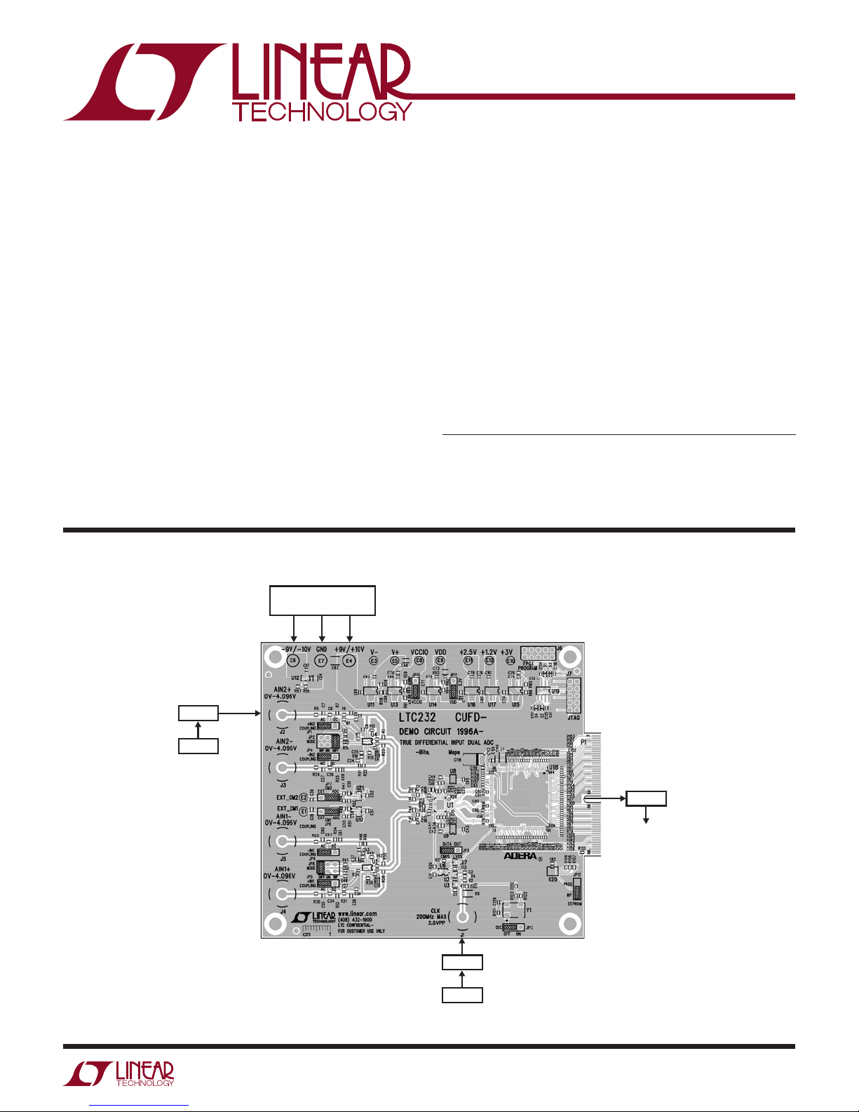
Figure 1. DC1996A Connection Diagram
dc1996afb
1
Page 2
DEMO MANUAL DC1996A
ASSEMBLY OPTIONS
Table 1. DC1996A Assembly Options
VERSION U1 PART NUMBER MAX CONVERSION RATE # OF BITS MAX CLOCK FREQUENCY
DC1996A-A LTC2323CUFD-16#PBF 5Msps 16 110MHz
DC1996A-B LTC2321CUFD-16#PBF 2Msps 16 64MHz
DC1996A-C LTC2323CUFD-14#PBF 5Msps 14 110MHz
DC1996A-D LTC2321CUFD-14#PBF 2Msps 14 62MHz
DC1996A-E LTC2323CUFD-12 #PBF 5Msps 12 95MHz
DC1996A-F LTC2321CUFD-12#PBF 2Msps 12 58MHz
QUICK START PROCEDURE
Demonstration circuit 1996A is easy to set up and evaluate
for performance. Refer to Figure 1 and follow the proce
dure below.
n
Connect the DC1996A to a DC890 USB high speed data
collection board using edge connector P1.
n
Connect the DC890 to a host PC with a standard USB
A/B cable.
n
Apply a low jitter signal source to J2 to test channel
2, or to J4 to test channel 1. Note that the DC1996A
is capable of accepting a differential input signal as
well as a single-ended signal. See the Hardware Setup
section for the jumper positions that correspond to
these configurations.
n
As a clock source, apply a low jitter 10dBm sine wave or
square wave to connector J1. See Table 1 for maximum
clock frequencies. Note that J1 has a 50Ω termination
resistor to ground.
n
Run the PScope software (Pscope.exe version K73,
or later) supplied with the DC890 or download it from
www.linear.com/software. Complete software doc-
umentation is available from the Help menu. Updates
can be downloaded from the Tools menu. Check for
updates periodically, as new features may be added.
The PScope software should recognize
-
and configure itself automatically.
n
Click the Collect button (Figure 2) to begin acquiring
the DC1996A
data. The Collect button then changes to Pause, which
can be used to stop data acquisition.
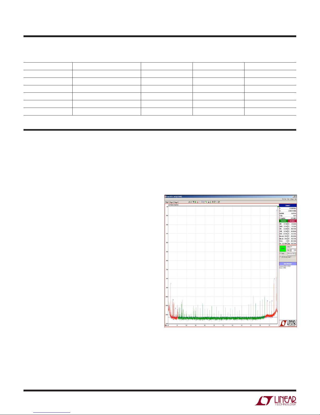
Figure 2. DC1996A PScope Screenshot
2
dc1996afb
Page 3

HARDWARE SETUP
DEMO MANUAL DC1996A
SIGNAL CONNECTIONS
J1 CLK IN: This input has a 50Ω termination resistor,
and is intended to be driven by a low jitter 10dBm sine or
square wave. To achieve the full AC performance of this
part, the clock jitter should be kept under 2ps. This input
is capacitively coupled so that the input clock can be either
0V to 3.3V or ±1.65V. This eliminates the need for level
shifting. To run at the maximum conversion rate, apply
the frequency specified in the Table 1.
J2 Ch2+ Input: In the single-ended configuration, this is
the channel 2 signal input. For differential operation, this
serves as the positive channel 2 signal input.
J3 Ch2– Input: This input is used only for differential
operation. It serves as the negative channel 2 signal input.
J4 Ch1+ Input: In the single-ended configuration, this is
the channel 1 signal input. For differential operation, this
serves as the positive channel 1 signal input.
J5 Ch1– Input: This input is used only for differential
operation. It serves as the negative channel 1 signal input.
J6 FPGA Program: Factory use only.
J7 JTAG: Factory use only.
JP1 +IN2 Coupling: Use this jumper to select AC- or DC-
coupling of the signal applied to J2.
is DC. At very low input frequencies, using AC-coupling
may degrade the distortion performance.
JP2 Mode: Use this jumper to select the signal input mode
for the channel 2 input of the LTC2323. The default setting
is Diff. The Diff setting accepts a single-ended signal from
J2 and applies it as a differential signal to channel 2 of the
LTC2323. The Bip setting accepts a single-ended signal
from J2 and applies it as a single-ended bipolar signal to
channel 2 of the LTC2323. The Uni setting also accepts a
single-ended signal from J2, but applies it as a unipolar
signal to channel 2 of the LTC2323.
The default setting
JP3 Data Out: Use this jumper to select the data output
format from the LTC2323. The default setting is CMOS.
The output data will not be valid if the jumper is moved
to the LVDS position unless the following changes have
been made:
Install 100Ω S0402 resistors at R26, 75, 76, 99
Reprogram the CPLD through J6 using the program
ming file LTC2323.pof found at:
http://www.linear.com/demo/DC1996A
Move JP3 to the LVDS position.
JP4 –IN2 Coupling: Use this jumper to select AC- or DCcoupling of the signal applied to J3. The default setting
is DC. At very low input frequencies, using AC-coupling
may degrade the distortion performance.
JP5 +IN1 Coupling: Use this jumper to select AC- or DCcoupling of the signal applied to J4. The default setting
is DC. At very low input frequencies, using AC-coupling
may degrade the distortion performance.
JP6 CM1: Use this jumper to set the DC bias point for the
signal applied to J4 when JP5 (+IN1 coupling) is in the
AC position. The default setting is ADC. The EXT setting
allows the use of an externally applied common mode
voltage applied at E1 (EXT_CM1).
JP7 CM2: Use this jumper to set the DC bias point for the
signal applied to J2 when JP1 (+IN2 coupling) is in the
AC position. The default setting is ADC. The EXT setting
allows the use of an externally applied common mode
voltage applied at E2 (EXT_CM2).
JP8 Mode: Use this jumper to select the signal input mode
for the channel 1 input of the LTC2323. The default setting
is Diff. The Diff setting accepts a single-ended signal from
J4 and applies it as a differential
LTC2323. The Bip setting accepts a single-ended signal
from J4 and applies it as a single-ended bipolar signal to
channel 1 of the LTC2323. The Uni setting also accepts a
single-ended signal from J4, but applies it as a unipolar
signal to channel 1 of the LTC2323.
signal to channel 1 of the
-
dc1996afb
3
Page 4
DEMO MANUAL DC1996A
HARDWARE SETUP
JP9 –IN1 Coupling: Use this jumper to select AC- or DCcoupling of the signal applied to J5. The default setting
is DC. At very low input frequencies, using AC-coupling
may degrade the distortion performance.
JP10 VCCIO: Use this jumper to select the VCCIO sup
ply voltage. The default setting is 2.5V. The 1.8V setting
selects a 1.8V supply voltage.
JP11 VDD: Use this jumper to select the VDD supply voltage. The default setting is 5V. The 3.3V setting selects a
3.3V supply voltage.
JP12 EEPROM: Factory use only.
-
JP13 OSC: Use this jumper to enable the onboard encode
clock source. The default setting
is OFF. The ON setting
energizes this source. Refer to the DC1996A schematic for
additional passive elements required to use the onboard
source.
PARTS LIST
ITEM QTY REFERENCE PART DESCRIPTION MANUFACTURER/PART NUMBER
Required Circuit Components
1 20 C1, C2, C4, C5, C9, C11, C13, C18, C19,
C22, C23, C29, C37, C51, C52, C58, C59,
C82, C129, C130
2 24 C3, C6, C16, C17, C20, C21, C24-C26,
C28, C30, C34, C47-C50, C53, C54, C57,
C61, C70, C76, C79, C81
3 0 C7, C8, C10, C14, C27, C35, C36, C40,
C41, C60
4 2 C12, C41 CAP., NPO, 200pF, 16V, 5%, 0603 MURAA, GRM1885C1H201JA01D
5 12 C15, C32, C38, C39, C43, C45, C65, C67,
C68, C71, C74, C77
6 6 C31, C33, C55, C56, C106, C119 CAP., X5R, 4.7µF, 6.3V, 10%, 0603 AVX, 06036D475K AT2A
7 2 C42, C44 CAP., X5R, 2.2µF, 10V, 10%, 0603 MURATA, GRM188R61A225KE34D
8 1 C62 CAP., X7R, 47µF, 10V, 10%, 1210 MURATA, GRM32ER71A476KE15L
9 5 C63, C69, C72, C75, C78 CAP., X7R, 0.01µF, 6.3V, 10%, 0603 MURATA, GRM188R70J103KA01D
10 3 C64, C66, C73 CAP., X7R, 10µF, 10V, 10%, 0805 MURATA, GRM21BR71A106KE51L
11 1 C80 CAP., X5R, 3.3µF
12 28 C83-C104, C108, C122-C126 CAP., X7R, 0.1µF, 16V, 10%, 0402 NIC, NMC0402X7R104K16TRPF
13 1 C105 CAP., X5R, 47µF, 6.3V, 20%, 0805 TAIYO YUDEN, JMK212BJ476MG-T
14 3 C107, C120, C121 CAP., X7R, 0.01µF, 16V, 10%, 0402 NIC, NMC0402X7R103K16TRPF
15 1 C109 CAP., X7R, 1nF, 16V, 10%, 0402 AVX, 0402YC102K AT2A
16 3 C110, C111, C112 CAP., X7R, 22nF, 16V, 10%, 0402 AVX, 0402YC223K AT2A
17 2 C113, C128 CAP., X7R, 4.7nF, 16V, 10%, 0402 AVX, 0402YC472KAT2A
18 4 C114, C115, C116, C117 CAP., NP0, 10pF, 16V, 10%, 0402 AVX, 0402YA100KAT2A
19 1 C118 CAP., TANT, 470µF 10V, 20%, 7343 AVX, TPSE477M010R0050
20 1 C127 CAP., X7R, 2.2nF, 16V, 10%, 0402 AVX, 0402YC222KAT2A
21 4 D1, D2, D3, D4 DIODE, SCHOTTKY, 30V, 200mW SOD-323 DIODE INC., BAT54WS-7-F
22 9 E1-E3, E5, E8-E12 TEST POINT, TURRET, 0.064" MILL-MAX, 2308-2-00-80-00-00-07-0
23 3 E4, E6, E7 TEST POINT, TURRET, 0.094" MILL-MAX, 2501-2-00-80-00-00-07-0
CAP., X7R, 0.1µF, 16V, 10%, 0603 NIC, NMC0603X7R104K16TRPF
CAP., X5R, 10µF, 6.3V, 20%, 0603 NIC, NMC0603X5R106M6.3TRPF4KF
CAP., 0603 OPT
CAP., X7R, 1µF, 25V, 10%, 0603 TDK, C1608X7R1E105K
, 6.3V, 10%, 0603 AVX, 06036D335K AT2A
dc1996afb
4
Page 5

DEMO MANUAL DC1996A
PARTS LIST
ITEM QTY REFERENCE PART DESCRIPTION MANUFACTURER/PART NUMBER
24 11 JP1, JP3-JP7, JP9-JP11, JP13, JP15 HEADER, 1×3, 0.100" SAMTEC, TSW-103-07-L-S
25 2 JP2, JP8 HEADER, 2×3, 0.100" SAMTEC, TSW-103-07-L-D
26 2 J6, J7 HEADER, 2×5, 0.100" SAMTEC, TSW-105-07-L-D
27 5 J1, J2, J3, J4, J5 CONN BNC FEM JACK PC MNT STRGHT AMPHENOL CONNEX, 112404
28 1 L1 IND, FERRITE CHIP, 390Ω, 2000mA, 1206 MURATA, BLM31PG391SN1L
29 15 R1, R2, R10, R21, R27, R46-R48, R51,
R52, R57, R58, R60, R64, R66
30 0 R3, R7, R11, R22, R23, R25, R28, R29,
R32, R34, R36, R37, R49, R50, R54,
R123
31 2 R4, R17 RES., CHIP, 33Ω, 1/10W, 5%, 0603 PANASONIC, ERJ-3GEYJ330V
RES., CHIP, 1k, 1/10W, 1%, 0603 PANASONIC, ERJ-3EKF1001V
RES., CHIP, 0603 OPT
32 11 R5, R6, R12, R20, R24, R30, R31, R35,
R39, R40, R53
33 4 R8, R18, R33, R44 RES., CHIP, 49.9Ω, 1/10W, 1%, 0603 PANASONIC, ERJ-3EKF49R9V
34 1 R9 RES., CHIP, 49.9Ω, 1/4W, 1%, 1206 PANASONIC, ERJ-8ENF49R9V,
35 4 R13, R16, R38, R43 RES., CHIP, 0Ω, 1/16W, 0402 PANASONIC, ERJ-2GE0R00X
36 4 R14, R15, R41, R42 RES., CHIP, 301, 1/10W, 1%, 0603 PANASONIC, ERJ-3EKF3010V
37 2 R19, R45 RES., CHIP, 150, 1/10W, 1%, 0603 PANASONIC, ERJ-3EKF1500V
38 0 R26, R75, R76, R99 RES., CHIP, 0402
39 2 R55, R56 RES., CHIP
40 1 R59 RES., CHIP, 499Ω, 1/10W, 1%, 0603 PANASONIC, ERJ-3EKF4990V
41 1 R61 RES., CHIP, 866Ω, 1/10W, 1%, 0603 PANASONIC, ERJ-3EKF8660V
42 1 R62 RES., CHIP, 3.09k, 1/10W, 1%, 0603 PANASONIC, ERJ-3EKF3091V
43 1 R63 RES., CHIP, 4.02k, 1/10W, 1%, 0603 PANASONIC, ERJ-3EKF4021V
44 1 R65 RES., CHIP, 1.43k, 1/10W, 1%, 0603 PANASONIC, ERJ-3EKF1431V
45 33 R69-R72, R77-R98, R100-R104, R119,
R120
46 1 R118 RES., CHIP, 1k, 1/16W, 1%, 0402 PANASONIC, ERJ-2EKF1001V
47 4 R105, R106, R107, R108 RES., CHIP, 4.99k, 1/10W, 1%, 0603 PANASONIC, ERJ-3EKF4991V
48 9 R109-R117 RES., CHIP, 10k, 1/16W, 5%, 0402 PANASONIC, ERJ-2GEYJ103V
49 1 R121 RES., CHIP, 10k, 1/16W, 5%, 0603 PANASONIC, ERJ-3GEYJ103V
50 1 R122 RES., CHIP, 100Ω, 1/10W, 1%, 0603 PANASONIC, ERJ-3EKF1000V
51 3 U2, U3, U7 IC, INVERTER, UHS, SINGLE, SC70-5 FAIRCHILD, NC7SZ04P5X
52 2 U4, U5 IC, 400MHz, AMPLIFIER, MS8 LINEAR TECHNOLOGY, LT1819CMS8#PBF
53 1 U6 IC, FLIP FLOP, D-TYPE LOG, US8 ON SEMI., NL17SZ74USG
54 2 U8, U9 IC, VOLTAGE REFERENCE, MSOP8 LINEAR TECHNOLOGY, LTC6655BHMS8-
55 2 U10, U21 IC, OP-AMP, MS8 LINEAR TECHNOLOGY, LT6202CS5#PBF
56 4 U11, U13, U14, U15 IC, MICROPOWER REGULATOR, SO8 LINEAR TECHNOLOGY, LT1763CS8#PBF
57 1 U12 IC, MICROPOWER NEG. REGULATOR,
58 1 U16 IC, MICROPOWER REGULATOR, SO8 LINEAR TECHNOLOGY, LT1763CS8-2.5#PBF
59 1 U17 IC, LINEAR REGULATOR, SO8 LINEAR TECHNOLOGY, LT3021ES8-1.2#PBF
RES., CHIP, 0Ω, 1/10W, 0603 PANASONIC, ERJ-3GEY0R00V
, 3.92k, 1/10W, 1%, 0603 PANASONIC, ERJ-3EKF3921V
RES., CHIP, 33Ω, 1/16W, 5%, 0402 PANASONIC, ERJ-2GEJ330X
4.096#PBF
LINEAR TECHNOLOGY, LT1964ES5-SD#PBF
SOT-23
dc1996afb
5
Page 6

DEMO MANUAL DC1996A
PARTS LIST
ITEM QTY REFERENCE PART DESCRIPTION MANUFACTURER/PART NUMBER
60 1 U18 IC, EQFP, CYCLONE3, WIRE BOND,
61 1 U19 IC, 4-BIT, FLASH MEMORY, SO8 ALTERA, EPCS4SI8
62 1 U20 IC, EEPROM, 2kBIT, 400kHz, 8TSSOP MICROCHIP, 24LC024-I/ST
63 1 Y1 OSCILLATOR, 106.2500MHz, 3.3V, SMD CTS-FREQUENCY CONTROLS, CB3LV -3I-
64 12 SHOWN ON ASSY DWG SHUNT, 0.100", 2POS SAMTEC, SNT-100-BK-G
65 4 MH1-MH4 STANDOFF, NYLON, 0.25" KEYSTONE, 8831 (SNAP-ON)
DC1996A-A Required Circuit Components
1 1 DC1996A GENERAL BOM
2 2 R67, R73 RES., CHIP, 1k, 1/16W, 5%, 0402 PANASONIC, ERJ-2EKF1001V
3 1 U1 I.C., DUAL SAR ADC, QFN28UFD-4X5 LINEAR TECHNOLOGY, LTC2323CUFD-16#PBF
DC1996A-B Required Circuit Components
1 1 DC1996A GENERAL BOM
2 2 R67, R73 RES., CHIP, 1k, 1/16W, 5%, 0402 PANASONIC, ERJ-2EKF1001V
3 1 U1 I.C., DUAL SAR ADC, QFN28UFD-4X5 LINEAR TECHNOLOGY, LTC2321CUFD-16#PBF
DC1996A-C Required Circuit Components
1 1 DC1996A GENERAL BOM
2 2 R68, R73 RES., CHIP, 1k, 1/16W, 5%, 0402 PANASONIC, ERJ-2EKF1001V
3 1 U1 I.C., DUAL SAR ADC, QFN28UFD-4X5 LINEAR TECHNOLOGY, LTC2323CUFD-14#PBF
DC1996A-D Required Circuit Components
1 1 DC1996A GENERAL BOM
2 2 R68, R73 RES., CHIP, 1k, 1/16W, 5%, 0402 PANASONIC, ERJ-2EKF1001V
3 1 U1 I.C., DUAL SAR
DC1996A-E Required Circuit Components
1 1 DC1996A GENERAL BOM
2 2 R67, R74 RES., CHIP, 1k, 1/16W, 5%, 0402 PANASONIC, ERJ-2EKF1001V
3 1 U1 I.C., DUAL SAR ADC, QFN28UFD-4X5 LINEAR TECHNOLOGY, LTC2323CUFD-12#PBF
DC1996A-F Required Circuit Components
1 1 DC1996A GENERAL BOM
2 2 R67, R74 RES., CHIP, 1k, 1/16W, 5%, 0402 PANASONIC, ERJ-2EKF1001V
3 1 U1 I.C., DUAL SAR ADC, QFN28UFD-4X5 LINEAR TECHNOLOGY, LTC2321CUFD-12#PBF
EQFP144
ADC, QFN28UFD-4X5 LINEAR TECHNOLOGY, LTC2321CUFD-14#PBF
ALTERA, EP3C5E144C7
106M2500
6
dc1996afb
Page 7

SCHEMATIC DIAGRAMS
5
4
3
2
1
D
C
B
A
04-01-14
04-01-14
04-01-14
R123
OPT
R123
OPT
R122
100
R122
C130
C130
NC7SZ04P5XU2NC7SZ04P5X
NC7SZ04P5XU3NC7SZ04P5X
R101kR10
1k
R9
49.9
1206R949.9
1206
0.1uF
0.1uF
100
2
3
OUT
GND
Y1
CB3LVY1CB3LV
EOH1VCC
4
+3V
C129
0.1uF
C129
0.1uF
+3V
C13
0.1uF
C13
0.1uF
53
VCCIOVCCIO VDD
C11
0.1uF
C11
0.1uF
VCCIO
2
1
C18
C18
C17
C17
C19
C19
C16
C16
C15
C15
DOUG S.PRODUCTION
DOUG S.PRODUCTION
DOUG S.PRODUCTION
1
REVISION HISTORY
DESCRIPTION DATEAPPROVEDECO REV
REVISION HISTORY
DESCRIPTION DATEAPPROVEDECO REV
REVISION HISTORY
DESCRIPTION DATEAPPROVEDECO REV
2
3
VCCIO VCCIO VCCIO
2
2
2
C2
0.1uFC20.1uF
53
C1
0.1uFC10.1uF
53
R21kR2
33
R433R4
1k
C5
0.1uFC50.1uF
J1J1
CLK
CLKIN
4
U2
2
4
U3
2
2.5VPP
200MHz MAX
R121
R121
0.1uF
0.1uF
10uF
10uF
0.1uF
0.1uF
10uF
10uF
1uF
1uF
DEMO MANUAL DC1996A
3
3
3
2
2
2
1
1
C45
1uF
C45
1uF
+9V/+10V+9V/+10V
1
2
4
VIN
GND3GND
E2
EXT_CM2E2EXT_CM2
E1
EXT_CM1E1EXT_CM1
U8
U8
C39
1uF
C39
1uF
U9
U9
C38
1uF
C38
1uF
SHDN
LTC6655BHMS8-4.096
LTC6655BHMS8-4.096
8
0
R400R40
R37
OPT
R37
OPT
132
CM2
CM2
JP7
JP7
EXT
EXT
ADC
ADC
C43
1uF
C43
1uF
1
2
VIN
GND3GND
SHDN
LTC6655BHMS8-4.096
LTC6655BHMS8-4.096
8
0
R390R39
R36
OPT
R36
OPT
132
CM1
CM1
JP6
JP6
EXT
EXT
ADC
ADC
VREF_2
4
VREF_1
GND5VOUT_S6VOUT_F7GND
C44
2.2uF
C44
2.2uF
C56
4.7uF
C56
0.1uF
0.1uF
0.1uF
0.1uF
R471kR47
1k
3
52
U21
U21
LT6202CS5
LT6202CS5
R461kR46
1k
3
52
U10
U10
LT6202CS5
LT6202CS5
4
+
+
1
VCM_BIAS_2VCM_BIAS_1
4
+
+
1
4.7uF
R521kR52
1k
-
-
C55
4.7uF
C55
4.7uF
R511kR51
1k
-
-
C49
10uF
6.3V
C49
10uF
6.3V
V+
C52
C52
GND5VOUT_S6VOUT_F7GND
C42
2.2uF
C42
2.2uF
C47
10uF
6.3V
C47
10uF
6.3V
V+
C51
C51
ON
OFF
ON
OFF
OSC
OSC
JP13
JP13
132
10k
10k
CSB
U7
NC7SZ04P5XU7NC7SZ04P5X
2
4
33
R1733R17
U6
7
8
NL17SZ74U6NL17SZ74
PR
D
Q
VCC
5
CP
Q
3
CLR
GND
6
4
6.3V
6.3V
C23
0.1uF
C23
0.1uF
C22
0.1uF
C22
0.1uF
6.3V
6.3V
132
JP3
JP3
DATA OUT
DATA OUT
LVDS
LVDS
CMOS
CMOS
R2033R20
33
REFOUT1
REFOUT2
ADD 20 MIL SQUARE
SDO1+
SDO1-
15
16
SDO1-
SDO1+
26
12
24
13
VDD2
8
VDD1
1
14
LVDS
25
AIN2+2AIN2-
AIN2+
PAD OPENING ON
TOP SOLDER MASK
LAYER ON THESE
CLKOUT+
SCK+
SCK-
9
21
22
17
18
SCK-
SCK+
CNVL
CLKOUT+
REFOUT2
VBYP2
VBYP1
*
*
QFN28UFD-4X5
QFN28UFD-4X5
U1
U1
OVDD
7
3
AIN2-
AIN1+
CONNETIONS.
CLKOUT-
SDO2+
SDO2-
20
19
SDO2-
SDO2+
CLKOUT-
REFRTN2
REFRTN111REFOUT1
GND
GND
GND
GND
GND
REFBG
AIN1-6AIN1+
AIN1-
C31 4.7uFC31 4.7uF
C33 4.7uFC33 4.7uF
27
29
23
10
5
4
C32
1uF
C32
1uF
28
R29
OPT
R29
OPT
www.linear.com
www.linear.com
www.linear.com
Fax: (408)434-0507
Milpitas, CA 95035
Phone: (408)432-1900
1630 McCarthy Blvd.
LTC Confidential-For Customer Use Only
Fax: (408)434-0507
Milpitas, CA 95035
Phone: (408)432-1900
1630 McCarthy Blvd.
LTC Confidential-For Customer Use Only
Fax: (408)434-0507
Milpitas, CA 95035
Phone: (408)432-1900
1630 McCarthy Blvd.
LTC Confidential-For Customer Use Only
TECHNOLOGY
TECHNOLOGY
TECHNOLOGY
V-
KIM T.
KIM T.
C59
0.1uF
C59
0.1uF
V-
C58
0.1uF
C58
0.1uF
KIM T.
APPROVALS
APPROVALS
APPROVALS
PCB DES.
PCB DES.
PCB DES.
CUSTOMER NOTICE
CUSTOMER NOTICE
CUSTOMER NOTICE
LINEAR TECHNOLOGY HAS MADE A BEST EFFORT TO DESIGN A
CIRCUIT THAT MEETS CUSTOMER-SUPPLIED SPECIFICATIONS;
HOWEVER, IT REMAINS THE CUSTOMER'S RESPONSIBILITY TO
VERIFY PROPER AND RELIABLE OPERATION IN THE ACTUAL
LINEAR TECHNOLOGY HAS MADE A BEST EFFORT TO DESIGN A
CIRCUIT THAT MEETS CUSTOMER-SUPPLIED SPECIFICATIONS;
HOWEVER, IT REMAINS THE CUSTOMER'S RESPONSIBILITY TO
VERIFY PROPER AND RELIABLE OPERATION IN THE ACTUAL
LINEAR TECHNOLOGY HAS MADE A BEST EFFORT TO DESIGN A
CIRCUIT THAT MEETS CUSTOMER-SUPPLIED SPECIFICATIONS;
HOWEVER, IT REMAINS THE CUSTOMER'S RESPONSIBILITY TO
VERIFY PROPER AND RELIABLE OPERATION IN THE ACTUAL
R73 R74
R68
1k OPT
R67
225
5A
Msps
161414
16
BITS
1
SHEET OF
SHEET OF
SHEET OF
LTC232XCUFD FAMILY
LTC232XCUFD FAMILY
LTC232XCUFD FAMILY
DEMO CIRCUIT 1996A
DEMO CIRCUIT 1996A
DEMO CIRCUIT 1996A
04/01/2014, 12:58 PM
04/01/2014, 12:58 PM
04/01/2014, 12:58 PM
IC NO. REV.
IC NO. REV.
IC NO. REV.
SCHEMATIC
SCHEMATIC
SCHEMATIC
TRUE DIFFERENTIAL INPUT DUAL ADC
TRUE DIFFERENTIAL INPUT DUAL ADC
TRUE DIFFERENTIAL INPUT DUAL ADC
B
B
B
SIZE
DATE:
SIZE
DATE:
SIZE
DATE:
TITLE:
TITLE:
TITLE:
DOUG S.
DOUG S.
DOUG S.
SCALE = NONE
SCALE = NONE
SCALE = NONE
APP ENG.
APP ENG.
APP ENG.
APPLICATION. COMPONENT SUBSTITUTION AND PRINTED
CIRCUIT BOARD LAYOUT MAY SIGNIFICANTLY AFFECT CIRCUIT
PERFORMANCE OR RELIABILITY. CONTACT LINEAR
TECHNOLOGY APPLICATIONS ENGINEERING FOR ASSISTANCE.
THIS CIRCUIT IS PROPRIETARY TO LINEAR TECHNOLOGY AND
SUPPLIED FOR USE WITH LINEAR TECHNOLOGY PARTS.
APPLICATION. COMPONENT SUBSTITUTION AND PRINTED
CIRCUIT BOARD LAYOUT MAY SIGNIFICANTLY AFFECT CIRCUIT
PERFORMANCE OR RELIABILITY. CONTACT LINEAR
TECHNOLOGY APPLICATIONS ENGINEERING FOR ASSISTANCE.
THIS CIRCUIT IS PROPRIETARY TO LINEAR TECHNOLOGY AND
SUPPLIED FOR USE WITH LINEAR TECHNOLOGY PARTS.
APPLICATION. COMPONENT SUBSTITUTION AND PRINTED
CIRCUIT BOARD LAYOUT MAY SIGNIFICANTLY AFFECT CIRCUIT
PERFORMANCE OR RELIABILITY. CONTACT LINEAR
TECHNOLOGY APPLICATIONS ENGINEERING FOR ASSISTANCE.
THIS CIRCUIT IS PROPRIETARY TO LINEAR TECHNOLOGY AND
SUPPLIED FOR USE WITH LINEAR TECHNOLOGY PARTS.
1k OPT
1k OPT OPT 1k
OPT 1k
5
2
12
R13
0 0402
R13
0 0402
C10
OPT
C10
OPT
R3
C4 0.1uFC4 0.1uF
V+
VCM_BIAS_2
R60R6
C3
10uF
R11kR1
1k
C6
C6
R50R5
OPTR3OPT
R8
49.9R849.9
1
U4A
U4A
LT1819CMS8
LT1819CMS8
84
+
-
+
-
3
2
C8
0
6.3VC310uF
6.3V
R7
6.3V
6.3V
10uF
10uF
C7
0
J2J2
AIN2+
0V - 4.096V
D
C9 0.1uFC9 0.1uF
OPTC8OPT
OPTR7OPT
OPTC7OPT
C12
C12
NP0
NP0
200pF
200pF
R15
301
R15
301
R12 0R12 0
V-
R14
301
R14
301
R11 OPTR11 OPT
2
MODE
135 6
DIFF
JP1
JP1
1
2
3
AC DC
AC DC
+IN2
+IN2
VREF_2
COUPLING
4
5
R16
R16
C14
C14
4
UNI
BIP
VCM_BIAS_2
0 0402
0 0402
OPT
OPT
JP2
HD2X3-100
JP2
HD2X3-100
C21
10uF
C21
10uF
C20
10uF
C20
10uF
R43
0 0402
R43
R38
R38
C40
C40
R28
OPT
R28
C29 0.1uFC29 0.1uF
V+
VCM_BIAS_1
R310R31
C30
10uF
C30
10uF
R271kR27
1k
C34
C34
R300R30
OPT
R33
R33
49.9
49.9
7
U5B
U5B
LT1819CMS8
LT1819CMS8
84
+
+
5
0
6.3V
6.3V
6.3V
6.3V
10uF
10uF
0
J4J4
AIN1+
0V - 4.096V
R35 0R35 0
C37 0.1uFC37 0.1uF
V-
-
-
6
C36
OPT
C36
OPT
R34 OPTR34 OPT
R32
OPT
R32
OPT
JP5
JP5
1
2
3
C35
OPT
C35
OPT
+IN1
+IN1
COUPLING
R23
OPT
R23
OPT
R18
49.9
R18
49.9
7
U4B
U4B
LT1819CMS8
LT1819CMS8
+
-
+
-
8 4
5
6
C25
10uF
C25
10uF
R22
OPT
R22
OPT
R19
150
R19
150
C28
10uF
6.3V
C28
10uF
6.3V
C24
10uF
6.3V
C24
10uF
6.3V
6.3V
6.3V
6.3V
6.3V
R211kR21
VCM_BIAS_2
R25
OPT
R25
OPT
1k
C26
C26
R240R24
10uF
10uF
6.3V
6.3V
0
J3J3
AIN2-
C27
OPT
C27
OPT
0V - 4.096V
C
JP4
JP4
1
2
3
AC DC
AC DC
-IN2
-IN2
COUPLING
0 0402
0 0402
0 0402
OPT
OPT
C46
OPT
C46
OPT
R50
OPT
R50
OPT
C41
C41
NP0
NP0
R44
49.9
R44
200pF
200pF
R42
R42
R41
R41
AC DC
AC DC
B
49.9
1
U5A
JP8
JP8
C50
C50
BIP
C48
C48
VCM_BIAS_1
-
-
2
HD2X3-100
HD2X3-100
10uF
6.3V
10uF
6.3V
10uF
6.3V
10uF
6.3V
R45
150
R45
150
U5A
LT1819CMS8
LT1819CMS8
+
+
8 4
3
C54
C54
R49
R49
C53
C53
R481kR48
VCM_BIAS_1
10uF
10uF
OPT
OPT
10uF
6.3V
10uF
6.3V
1k
C57
C57
6.3V
6.3V
10uF
10uF
0
R530R53
J5J5
AIN1-
0V - 4.096V
301
301
301
301
4
2
MODE
135 6
DIFF
UNI
VREF_1
U1
LTC2323CUFD-12 12
LTC2323CUFD-16
LTC2321CUFD-16
LTC2321CUFD-14D
LTC2323CUFD-14
E
F LTC2321CUFD-12
B
C
ASSY
*
C61
10uF
6.3V
C61
10uF
6.3V
R54
OPT
R54
OPT
JP9
JP9
1
2
3
AC DC
AC DC
C60
OPT
C60
OPT
-IN1
-IN1
COUPLING
1. ALL RESISTORS ARE IN OHMS, 0603.
ALL CAPACITORS ARE IN MICROFARADS, 0603
NOTES: UNLESS OTHERWISE SPECIFIED
A
dc1996afb
7
Page 8

DEMO MANUAL DC1996A
5
4
3
2
1
D
C
B
A
SCHEMATIC DIAGRAMS
D
C
B
A
www.linear.com
www.linear.com
www.linear.com
3
3
3
2
2
2
2
2
2
SHEET OF
SHEET OF
SHEET OF
1
2
E3E3
5
U12
LT1964ES5-SD
U12
LT1964ES5-SD
-9V/-10V
V-
V-
C64
10uF
10V
C64
10uF
10V
R55
3.92k
R55
3.92k
4
ADJ
OUT
GND1IN2SHDN
3
C67
C67
E6E6
0805
0805
R571kR57
1k
1uF
16V
1uF
16V
Fax: (408)434-0507
Milpitas, CA 95035
Phone: (408)432-1900
1630 McCarthy Blvd.
LTC Confidential-For Customer Use Only
Fax: (408)434-0507
Milpitas, CA 95035
Phone: (408)432-1900
1630 McCarthy Blvd.
LTC Confidential-For Customer Use Only
Fax: (408)434-0507
Milpitas, CA 95035
Phone: (408)432-1900
1630 McCarthy Blvd.
LTC Confidential-For Customer Use Only
LTC232XCUFD-16/-14 FAMILY
LTC232XCUFD-16/-14 FAMILY
LTC232XCUFD-16/-14 FAMILY
DEMO CIRCUIT 1996A
DEMO CIRCUIT 1996A
TECHNOLOGY
TECHNOLOGY
TECHNOLOGY
APPROVALS
APPROVALS
APPROVALS
CUSTOMER NOTICE
CUSTOMER NOTICE
CUSTOMER NOTICE
LINEAR TECHNOLOGY HAS MADE A BEST EFFORT TO DESIGN A
CIRCUIT THAT MEETS CUSTOMER-SUPPLIED SPECIFICATIONS;
LINEAR TECHNOLOGY HAS MADE A BEST EFFORT TO DESIGN A
CIRCUIT THAT MEETS CUSTOMER-SUPPLIED SPECIFICATIONS;
LINEAR TECHNOLOGY HAS MADE A BEST EFFORT TO DESIGN A
CIRCUIT THAT MEETS CUSTOMER-SUPPLIED SPECIFICATIONS;
DEMO CIRCUIT 1996A
04/01/2014, 01:00 PM
04/01/2014, 01:00 PM
04/01/2014, 01:00 PM
IC NO. REV.
IC NO. REV.
IC NO. REV.
SCHEMATIC
SCHEMATIC
SCHEMATIC
TRUE DIFFERENTIAL INPUT DUAL ADC
TRUE DIFFERENTIAL INPUT DUAL ADC
TRUE DIFFERENTIAL INPUT DUAL ADC
B
B
B
SIZE
DATE:
SIZE
DATE:
SIZE
DATE:
TITLE:
TITLE:
TITLE:
KIM T.
KIM T.
KIM T.
DOUG S.
DOUG S.
DOUG S.
SCALE = NONE
SCALE = NONE
PCB DES.
PCB DES.
PCB DES.
HOWEVER, IT REMAINS THE CUSTOMER'S RESPONSIBILITY TO
VERIFY PROPER AND RELIABLE OPERATION IN THE ACTUAL
HOWEVER, IT REMAINS THE CUSTOMER'S RESPONSIBILITY TO
VERIFY PROPER AND RELIABLE OPERATION IN THE ACTUAL
HOWEVER, IT REMAINS THE CUSTOMER'S RESPONSIBILITY TO
VERIFY PROPER AND RELIABLE OPERATION IN THE ACTUAL
SCALE = NONE
APP ENG.
APP ENG.
APP ENG.
APPLICATION. COMPONENT SUBSTITUTION AND PRINTED
CIRCUIT BOARD LAYOUT MAY SIGNIFICANTLY AFFECT CIRCUIT
PERFORMANCE OR RELIABILITY. CONTACT LINEAR
TECHNOLOGY APPLICATIONS ENGINEERING FOR ASSISTANCE.
THIS CIRCUIT IS PROPRIETARY TO LINEAR TECHNOLOGY AND
SUPPLIED FOR USE WITH LINEAR TECHNOLOGY PARTS.
APPLICATION. COMPONENT SUBSTITUTION AND PRINTED
CIRCUIT BOARD LAYOUT MAY SIGNIFICANTLY AFFECT CIRCUIT
PERFORMANCE OR RELIABILITY. CONTACT LINEAR
TECHNOLOGY APPLICATIONS ENGINEERING FOR ASSISTANCE.
THIS CIRCUIT IS PROPRIETARY TO LINEAR TECHNOLOGY AND
SUPPLIED FOR USE WITH LINEAR TECHNOLOGY PARTS.
APPLICATION. COMPONENT SUBSTITUTION AND PRINTED
CIRCUIT BOARD LAYOUT MAY SIGNIFICANTLY AFFECT CIRCUIT
PERFORMANCE OR RELIABILITY. CONTACT LINEAR
TECHNOLOGY APPLICATIONS ENGINEERING FOR ASSISTANCE.
THIS CIRCUIT IS PROPRIETARY TO LINEAR TECHNOLOGY AND
SUPPLIED FOR USE WITH LINEAR TECHNOLOGY PARTS.
-9V/-10V
3
V+
E5E5
C66
10uF
10V
0805
C66
10uF
10V
0805
V+
R56
3.92k
R56
3.92k
R581kR58
1k
C63
0.01uF
C63
0.01uF
1
2
U11
U11
LT1763CS8
LT1763CS8
4
SEN
BYP
OUT
GND
7
GND
6
GND
3
SHDN
IN
5
8
C65
1uF
16V
C65
1uF
16V
4
VCCIO
U13
U13
LT1763CS8
LT1763CS8
E8E8
VCCIO
1
OUT
IN
8
C70
10uF
6.3V
C70
10uF
6.3V
2.5V
1.8V
JP10JP10
VCCIO
132
R59
499
R59
499
C69
0.01uF
C69
0.01uF
2
4
SEN
BYP
GND
7
GND
6
GND
3
SHDN
5
C68
1uF
16V
C68
1uF
16V
VDD
E9E9
C73
10uF
10V
0805
C73
10uF
10V
0805
VDD
3.3V
VDD
R61
866
R61
866
R601kR60
1k
U14
U14
LT1763CS8
LT1763CS8
132
R63
4.02k
R63
4.02k
R62
3.09k
R62
3.09k
C72
0.01uF
C72
0.01uF
1
2
4
SEN
BYP
OUT
GND
7
GND
6
GND
3
SHDN
IN
5
8
C71
1uF
16V
C71
1uF
16V
+3V
E10E10
C76
10uF
6.3V
C76
10uF
6.3V
+3V
5V
JP11JP11
R661kR66
R65
1.43k
R65
R641kR64
1.43k
1k
C75
C75
0.01uF
0.01uF
1
2
4
SEN
BYP
OUT
GND
7
GND
6
GND
3
SHDN
IN
U15
U15
LT1763CS8
LT1763CS8
5
8
C74
1uF
16V
C74
1uF
16V
+2.5V
E11E11
C79
10uF
6.3V
C79
10uF
6.3V
+2.5V
1k
C78
0.01uF
C78
0.01uF
1
2
4
SEN
BYP
OUT
GND
7
GND
6
GND
3
SHDN
IN
U16
U16
LT1763CS8-2.5
LT1763CS8-2.5
5
8
C77
1uF
16V
C77
1uF
16V
E12E12
+1.2V
U17
LT3021ES8-1.2
U17
LT3021ES8-1.2
2
8
+1.2V
C81
C81
VCCINT
OUT
IN
C80
C80
10uF
6.3V
10uF
6.3V
3
SEN
AGND
4
GND
6
SHDN
5
3.3uF
16V
3.3uF
16V
C62
47uF
1210
16V
C62
47uF
1210
16V
+9V/+10V
E4E4
5
E7E7
GND
+9V/+10V
8
dc1996afb
Page 9

SCHEMATIC DIAGRAMS
5
4
3
2
1
D
C
B
A
D
1
135791113151719212325272931333537394143454749515355575961636567697173757779818385878991939597
P1
P1
246
8
101214161820222426283032343638404244464850525456586062646668707274767880828486889092949698
CNVCLK
DB0
DB1
DB2
DB3
DB4
DB5
DB6
DB7
DB8
DB9
DB10
DB11
DB12
DB13
DB14
DB15
2
SDO1-
SDO1+
CLKOUT+
CLKOUT-
R76
OPT
R76
OPT
R99
OPT
R99
OPT
54
55
58
59
60
64
65
66
67
69
70
72
71
IO3
IO6
IO1068IO11
IO8_RUP2
IO7_VREF4
IO5_DIFFIOB16N
SDO2-
R75
OPT
R75
OPT
44
46
49
50
51
IO6_VREF3
IO7_DIFFIOB9P
IO8_DIFFIOB9N
31
32
33
34
IO6
IO4_RUP1
IO5_RDN1
IO3_VREF2
SCK+
DB15
R26
OPT
R26
OPT
33R119 33R119
7
10
11
23
CLK022CLK1
IO5_VREF1
IO6_DIFFL4P
IO7_DIFFL4N
IO9_RDN2
IO12_DIFFIOB21P
IO13_DIFFIOB21N
SDO2+
52
53
IO9
IO10_DIFFIOB11P
IO11_DIFFIOB11N
SCK-
IO14
CLKIN
CYCLONE3-EP3C5E144
CYCLONE3-EP3C5E144
CYCLONE3-EP3C5E144
CYCLONE3-EP3C5E144
CYCLONE3-EP3C5E144
CYCLONE3-EP3C5E144
CYCLONE3-EP3C5E144
CYCLONE3-EP3C5E144
BANK4
BANK4
IO1_DIFFIOB12P
IO4_DIFFIOB16P
IO2_DIFFIOB12N
U18E
U18E
3
38
39
IO342IO443IO5
BANK3
BANK3
IO1_DIFFIOB1P
IO2_DIFFIOB1N
U18D
U18D
4
25
30
IO128IO2
CLK224CLK3
BANK2
BANK2
U18C
U18C
DB12
DB13
DB14
CNVCLK
33R69 33R69
33R70 33R70
33R71 33R71
33R72 33R72
5
U18B
U18B
BANK1
BANK1
4
IO11IO22IO33IO4
DA15
U18I
U18I
U18H
U18H
U18G
U18G
U18F
U18F
DA12
DA13
DA14
DB1
DB2
DB3
DB4
33R91 33R91
33R88 33R88
33R81 33R81
33R79 33R79
128
129
132
133
BANK8
BANK8
IO2_DIFFIOT11P
IO1_DIFFIOT11N
IO3_DIFFIOT10N
DA6
DA7
DA8
DA9
33R90 33R90
33R87 33R87
33R78 33R78
33R80 33R80
110
111
112
113
IO1
IO2
IO3
BANK7
BANK7
DA4
33R89 33R89
33R86 33R86
90
91
100
104
IO1
BANK6
BANK6
CLK4_DIFFCLK2P
CLK5_DIFFCLK2N
DA0
DA1
DA2 DA3
33R85 33R85
33R84 33R84
33R77 33R77
75
76
IO173IO274IO3
BANK5
BANK5
DA8
DA9
DA10
DA11
DB5
DB6
DB7
DB8
33R96 33R96
33R94 33R94
33R92 33R92
33R82 33R82
135
136
137
138
141
IO5
IO7
IO8
IO9
IO6_VREF8
IO4_DIFFIOT10P
DA12
DA10
DA11
33R97 33R97
33R95 33R95
33R93 33R93
114
115
119
120
121
IO4
IO5_RUP4
IO6_RDN4
IO7_VREF7
IO9_DIFFIOT16P
IO8_DIFFIOT16N
DA5
33R83 33R83
105
106
IO2
IO4
IO3_VREF6
CSB
VCCIO
*
R73*R73
77
79
80
84
83
IO5
IO7
IO4_RUP3
IO4_RDN3
IO6_VREF5
IO8_DIFFIOR8N
C
DA5
DA6
DA7
DB9
DB10
DB11
33R103 33R103
33R101 33R101
33R98 33R98
142
143
144
IO10
IO12_DIFFIOT01P
IO11_DIFFIOT01N
DA13
DA14
DB0
DA15
33R104 33R104
33R102 33R102
33R120 33R120
33R100 33R100
124
125
126
127
IO10
IO11
IO13_DIFFIOT12P
IO12_DIFFIOT12N
*
R74*R74
85
88
89
IO9_DIFFIOR8P
CLK6_DIFFCLK3P
CLK7_DIFFCLK3N
DA4
R67*R67
VCCIO
VCCIO
DA2
DA3
*
R105
4.99k
R105
4.99k
99
100
DA0
DA1
CYCLONE3-EP3C5E144
CYCLONE3-EP3C5E144
CYCLONE3-EP3C5E144
CYCLONE3-EP3C5E144
CYCLONE3-EP3C5E144
CYCLONE3-EP3C5E144
R68*R68
*
CYCLONE3-EP3C5E144
CYCLONE3-EP3C5E144
DEMO MANUAL DC1996A
0603
0603
EDGE-CON-100
EDGE-CON-100
1356
FPGA
PROGRAM
2
+3V
B
PROG
WP
PROG
WP
JP12
JP12
EEPROM
EEPROM
5
3
7
6
WP
SCL
SDA
U20
U20
24LC024-I /ST
24LC024-I /ST
VCC
8
C92
0.1uF
0402
C92
0.1uF
0402
C91
0.1uF
0402
C91
0.1uF
0402
+3V +3V
5
8
7
6
VCC
VCC
ASDI
DCLK
NCS1DATA2VCC3GND
U19
U19
4
+3V
10k
10k
10k
10k
10k
10k
10k
10k
10k
10k
10k
10k
6
8
9
12
13
14
DCLK
CONFIG
CONFIG
N_STATUS
IO1_DATA1
IO3_DATA0
IO2_FLASH_NCE
C90
C90
0.1uF
0.1uF
C89
C89
0.1uF
0.1uF
C88
C88
0.1uF
0.1uF
C87
C87
0.1uF
0.1uF
C86
C86
0.1uF
0.1uF
C85
C85
0.1uF
0.1uF
C84
C84
0.1uF
0.1uF
C83
C83
VCCIO
0.1uF
0.1uF
102
116
134
VCCINT5VCCINT29VCCINT45VCCINT61VCCINT78VCCINT
VCCINT
PWR
PWR
GND19GND27GNDA136GND41GND48GND57GND63GND82GND95GNDA2
132
A01A12A2
ARRAY
ARRAY
EEPROM
EEPROM
GND
4
EPCS4SI8
EPCS4SI8
TDI
TMS
TCK
TDO
NCE
15
16
21
86
87
92
TDI
TCK
TMS18TDO20NCE
NCONFIG
IO4_DEV_OE
IO5_DEV_CLRN
C104
C104
0.1uF
0.1uF
C103
C103
0.1uF
0.1uF
C102
C102
0.1uF
0.1uF
C101
C101
0.1uF
0.1uF
C100
C100
0.1uF
0.1uF
C99
C99
0.1uF
0.1uF
C98
C98
0.1uF
0.1uF
C97
C97
0.1uF
0.1uF
C96
C96
0.1uF
0.1uF
C95
C95
0.1uF
0.1uF
C94
C94
0.1uF
0.1uF
C93
C93
0.1uF
0.1uF
VCCINT
VCCIO117VCCIO226VCCIO340VCCIO347VCCIO456VCCIO462VCCIO581VCCIO693VCCIO7
GND
GND
GND
108
118
123
131
140
+3V +3V +3V +3V
+2.5V
97
98
MSEL094MSEL196MSEL2
CONF_DONE
+2.5V
117
122
130
139
VCCIO7
VCCIO8
GND
GND
145
D4
12
D3
12
D2
12
D1
12
R1181kR118
1k
R117
10k
R117
10k
R116
10k
R116
10k
R115
10k
R115
10k
99
101
103
IO8_NCEO
IO9_CLKUSR
IO6_INIT_DONE
IO7_CRC_ERROR
CYCLONE3-EP3C5E144
CYCLONE3-EP3C5E144
C113
C113
4.7nF
4.7nF
C112
C112
22nF
22nF
C111
C111
22nF
22nF
C110
C110
22nF
22nF
C109
C109
1nF
1nF
C108
C108
0.1uF
0.1uF
C107
C107
0.01uF
0.01uF
C106
C106
4.7uF
4.7uF
C105
C105
47uF
47uF
107
109
VCCA135VCCA2
VCCIO8
VCCD_PLL137VCCD_PLL2
BAT54WSD4BAT54WS
BAT54WSD3BAT54WS
BAT54WSD2BAT54WS
BAT54WSD1BAT54WS
0603
0603
0805
0805
CYCLONE3-EP3C5E144
CYCLONE3-EP3C5E144
R108
4.99k
0603
R108
4.99k
0603
R107
4.99k
0603
R107
4.99k
0603
R106
4.99k
0603
R106
4.99k
0603
C82
0.1uF
0603
C82
0.1uF
0603
7
9
J6
HD2X5-100J6HD2X5-100
4
8
10
R114
R114
R113
R113
R112
R112
R111
R111
R110
R110
R109
R109
VCCIO
U18J
U18J
+1.2V
U18A
U18A
A
www.linear.com
www.linear.com
www.linear.com
Fax: (408)434-0507
Milpitas, CA 95035
Phone: (408)432-1900
1630 McCarthy Blvd.
LTC Confidential-For Customer Use Only
Fax: (408)434-0507
Milpitas, CA 95035
Phone: (408)432-1900
1630 McCarthy Blvd.
LTC Confidential-For Customer Use Only
Fax: (408)434-0507
Milpitas, CA 95035
Phone: (408)432-1900
1630 McCarthy Blvd.
LTC Confidential-For Customer Use Only
TECHNOLOGY
TECHNOLOGY
TECHNOLOGY
SCHEMATIC
SCHEMATIC
SCHEMATIC
TITLE:
TITLE:
TITLE:
KIM T.
KIM T.
KIM T.
DOUG S.
DOUG S.
DOUG S.
APPROVALS
APPROVALS
APPROVALS
PCB DES.
PCB DES.
PCB DES.
APP ENG.
APP ENG.
C117
10pF
C117
10pF
C116
10pF
C116
10pF
C115
10pF
C115
10pF
C114
10pF
C114
10pF
JTAG
VCCIO
+1.2V
L1
L1
BLM31PG391SN1L
BLM31PG391SN1L
VCCD_PLL
APP ENG.
CUSTOMER NOTICE
CUSTOMER NOTICE
CUSTOMER NOTICE
LINEAR TECHNOLOGY HAS MADE A BEST EFFORT TO DESIGN A
CIRCUIT THAT MEETS CUSTOMER-SUPPLIED SPECIFICATIONS;
HOWEVER, IT REMAINS THE CUSTOMER'S RESPONSIBILITY TO
VERIFY PROPER AND RELIABLE OPERATION IN THE ACTUAL
APPLICATION. COMPONENT SUBSTITUTION AND PRINTED
CIRCUIT BOARD LAYOUT MAY SIGNIFICANTLY AFFECT CIRCUIT
TDI
TCK
TDO
TMS
1356
7
9
J7
HD2X5-100J7HD2X5-100
4
2
8
10
C128
C128
4.7nF
4.7nF
C127
C127
2.2nF
2.2nF
C126
C126
0.1uF
0.1uF
C125
C125
0.1uF
0.1uF
C124
C124
0.1uF
0.1uF
C123
C123
0.1uF
0.1uF
C122
C122
0.1uF
0.1uF
C121
C121
0.01uF
0.01uF
C120
C120
0.01uF
0.01uF
C119
0603
C119
0603
4.7uF
4.7uF
C118
7343+C118
7343
470uF
470uF
+
3
3
3
2
2
2
3
3
3
SHEET OF
SHEET OF
SHEET OF
LTC232XCUFD-16/-14 FAMILY
LTC232XCUFD-16/-14 FAMILY
LTC232XCUFD-16/-14 FAMILY
DEMO CIRCUIT 1996A
DEMO CIRCUIT 1996A
DEMO CIRCUIT 1996A
04/01/2014, 12:59 PM
04/01/2014, 12:59 PM
04/01/2014, 12:59 PM
IC NO. REV.
IC NO. REV.
IC NO. REV.
TRUE DIFFERENTIAL INPUT DUAL ADC
TRUE DIFFERENTIAL INPUT DUAL ADC
TRUE DIFFERENTIAL INPUT DUAL ADC
B
B
B
SIZE
DATE:
SIZE
DATE:
SIZE
DATE:
SCALE = NONE
SCALE = NONE
SCALE = NONE
PERFORMANCE OR RELIABILITY. CONTACT LINEAR
TECHNOLOGY APPLICATIONS ENGINEERING FOR ASSISTANCE.
THIS CIRCUIT IS PROPRIETARY TO LINEAR TECHNOLOGY AND
SUPPLIED FOR USE WITH LINEAR TECHNOLOGY PARTS.
PERFORMANCE OR RELIABILITY. CONTACT LINEAR
TECHNOLOGY APPLICATIONS ENGINEERING FOR ASSISTANCE.
THIS CIRCUIT IS PROPRIETARY TO LINEAR TECHNOLOGY AND
SUPPLIED FOR USE WITH LINEAR TECHNOLOGY PARTS.
PERFORMANCE OR RELIABILITY. CONTACT LINEAR
TECHNOLOGY APPLICATIONS ENGINEERING FOR ASSISTANCE.
THIS CIRCUIT IS PROPRIETARY TO LINEAR TECHNOLOGY AND
SUPPLIED FOR USE WITH LINEAR TECHNOLOGY PARTS.
1. ALL RESISTORS AND CAPACITORS ON THIS PAGE ARE 0402.
NOTES: UNLESS OTHERWISE SPECIFIED
2. SEE ASSEMBLY TABLE ON PAGE 1 FOR R67, R68, R73, AND R74 VALUES.
dc1996afb
Information furnished by Linear Technology Corporation is believed to be accurate and reliable.
However, no responsibility is assumed for its use. Linear Technology Corporation makes no representation that the interconnection of its circuits as described herein will not infringe on existing patent rights.
9
Page 10

DEMO MANUAL DC1996A
DEMONSTRATION BOARD IMPORTANT NOTICE
Linear Technology Corporation (LT C ) provides the enclosed product(s) under the following AS IS conditions:
This demonstration board (DEMO BOARD) kit being sold or provided by Linear Technology is intended for use for ENGINEERING DEVELOPMENT
OR EVALUATION PURPOSES ONLY and is not provided by LT C for commercial use. As such, the DEMO BOARD herein may not be complete
in terms of required design-, marketing-, and/or manufacturing-related protective considerations, including but not limited to product safety
measures typically found in finished commercial goods. As a prototype, this product does not fall within the scope of the European Union
directive on electromagnetic compatibility and therefore may or may not meet the technical requirements of the directive, or other regulations.
If this evaluation kit does not meet the specifications recited in the DEMO BOARD manual the kit may be returned within 30 days from the date
of delivery for a full refund. THE FOREGOING WARRANTY IS THE EXCLUSIVE WARRANTY MADE BY THE SELLER TO BUYER AND IS IN LIEU
OF ALL OTHER WARRANTIES, EXPRESSED, IMPLIED, OR STATUTORY, INCLUDING ANY WARRANTY OF MERCHANTABILITY OR FITNESS
FOR ANY PARTICULAR PURPOSE. EXCEPT TO THE EXTENT OF THIS INDEMNITY, NEITHER PARTY SHALL BE LIABLE TO THE OTHER FOR
ANY INDIRECT, SPECIAL, INCIDENTAL, OR CONSEQUENTIAL DAMAGES.
The user assumes all responsibility and liability for proper and safe handling of the goods. Further, the user releases LTC from all claims
arising from the handling or use of the goods. Due to the open construction of the product, it is the user’s responsibility to take any and all
appropriate precautions with regard to electrostatic discharge. Also be aware that the products herein may not be regulatory compliant or
agency certified (FCC, UL, CE, etc.).
No License is granted under any patent right or other intellectual property whatsoever. LTC assumes no liability for applications assistance,
customer product design, software performance, or infringement of patents or any other intellectual property rights of any kind.
LT C currently services a variety of customers for products around the world, and therefore this transaction is not exclusive.
Please read the DEMO BOARD manual prior to handling the product. Persons handling this product must have electronics training and
observe good laboratory practice standards. Common sense is encouraged.
This notice contains important safety information about temperatures and voltages. For further safety concerns, please contact a LTC application engineer.
Mailing Address:
Linear Technology
1630 McCarthy Blvd.
Milpitas, CA 95035
Copyright © 2004, Linear Technology Corporation
Linear Technology Corporation
10
1630 McCarthy Blvd., Milpitas, CA 95035-7417
(408) 432-1900 ● FAX: (408) 434-0507 ● www.linear.com
dc1996afb
LT 0414 REV B • PRINTED IN USA
LINEAR TECHNOLOGY CORPORATION 2014
Page 11

Mouser Electronics
Authorized Distributor
Click to View Pricing, Inventory, Delivery & Lifecycle Information:
Analog Devices Inc.:
DC1996A-C DC1996A-E DC1996A-F DC1996A-A DC1996A-B DC1996A-D
 Loading...