

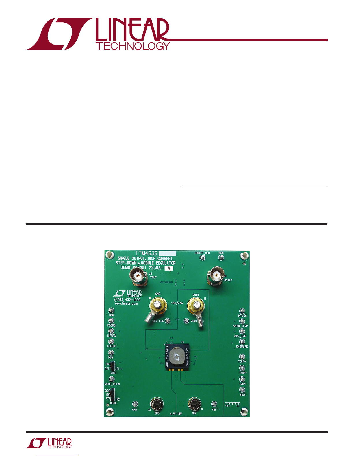
Page 1
DESCRIPTION
DEMO MANUAL DC2230A-A
LTM4636
40A DC/DC µModule Regulator
Demonstration circuit 2230A-A features the LTM®4636EY,
a 40A high efficiency, switch mode step-down power
µModule
15V. For input voltage range from 4.7V to 5.5V, short PV
pin to V
output voltage range is 0.6V to 3.3V. Derating is necessary
for certain V
board operates in continuous conduction mode in heavy
load conditions. For high efficiency at low load currents,
the MODE_PLLIN jumper selects pulse-skipping mode for
noise sensitive applications or BurstMode
less noise sensitive applications. The MODE_PLLIN pin
®
regulator. The input voltage range is from 4.7V to
pin with R8 = R21 = 0Ω and remove R17. The
IN
, V
IN
, frequency and thermal conditions. The
OUT
®
operation in
CC
BOARD PHOTO
also allows the LTM4636 to synchronize to an external
clock signal. DC2230A-A has the option of choosing both
internal and external compensation circuit for LTM4636.
Tying the PHASMD pin to different voltage generates cer
tain phase difference between MODE_PLLIN and CLKOUT.
The LTM4636
this demo manual prior to working on or modifying demo
circuit DC2230A-A.
Design files for this circuit board are available at
http://www.linear.com/demo/DC2230A-A
L, LT, LTC, LTM, Linear Technology, the Linear logo, Burst Mode and μModule are registered
trademarks of Linear Technology Corporation. All other trademarks are the property of their
respective owners.
data sheet must be read in conjunction with
-
dc2330aaf
1
Page 2
DEMO MANUAL DC2230A-A
PERFORMANCE SUMMARY
PARAMETER CONDITIONS/NOTES VALUE
Input Voltage Range 4.7V to 15V
Output Voltages 1.0V ± 1.3%
Maximum Continuous Output Current Derating is Necessary for Certain Operating Conditions. See Data Sheet for Details. 40ADC
Operating Frequency 350kHz
Efficiency V
Load Transient V
= 12V, V
IN
= 12V, V
IN
= 1.0V, I
OUT
= 1.0V, I
OUT
= 40A 87.7% (see Figure 2)
OUT
= 0A to 10A 81mV (see Figure 3)
STEP
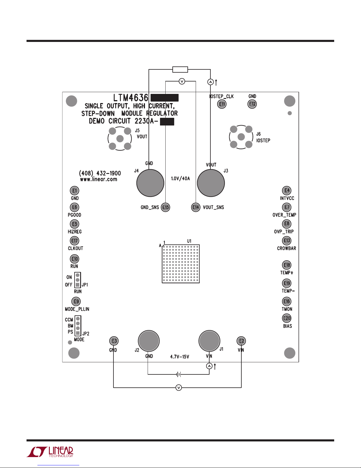
QUICK START PROCEDURE
Vary the input voltage from 6V to 15V and adjust the
Demonstration circuit 2230A-A is an easy way to evaluate the performance of the LTM4636EY. Please refer to
Figure1
for proper measurement equipment setup and
follow the procedure below.
4.
load current from 0A – 40A. Observe the output voltage regulation, ripple voltage, efficiency, and other
parameters.
1. Place jumpers in the following positions for a typical
application:
MODE RUN
CCM ON
2. With power off, connect the input power supply, load
and meters as shown in Figure 1. Preset the load to 0A
and V
supply to 12V.
IN
3. Turn on the power supply at the input. The output voltage should be 1.0V ± 1.3% (0.987V to 1.013V).
(Optional) For optional load transient test, apply an
5.
adjustable pulse signal between IOSTEP_CLK and GND
test points. The pulse amplitude sets the load step cur
rent amplitude. Keep the pulse width short (<1ms) and
<
pulse duty cycle low (
5%) to limit the thermal stress
on the load transient circuit.
6. (Optional) LTM4636 can be synchronized to an external
clock signal. Place the JP1 jumper on EXT_CLK and
apply a clock signal (0V to 5V, square wave) on the
MODE_PLLIN test point.
-
2
dc2230aaf
Page 3
+
–
+
–
+
–
QUICK START PROCEDURE
DEMO MANUAL DC2230A-A
LOAD
+
–
Figure 1. Measurement Setup of DC2230A-A
dc2330aaf
3
Page 4

DEMO MANUAL DC2230A-A
OUTPUT CURRENT (A)
0510152025303540010
2030405060708090100
EFFICIENCY (%)
dc2230aa F02
QUICK START PROCEDURE
12V
5V
IN
IN
V
50mV/DIV
I
OUT_STEP
10A/DIV
OUT
Figure 2. Measured Efficiency at VIN = 5V/12V, V
= 1V, fSW = 350kHz, CCM
OUT
Figure 3. Measured Load Transient, VIN = 12V, V
4
= 1.0V, I
OUT
= 0A to 10A
STEP
dc2230aaf
Page 5

QUICK START PROCEDURE
DEMO MANUAL DC2230A-A
Figure 4. Thermal Image of LTM4636, VIN = 12V, V
= 1.0V, I
OUT
= 40A, Ambient Temperature = 23.0°C, No Forced Airflow
LOAD
dc2330aaf
5
Page 6

DEMO MANUAL DC2230A-A
PARTS LIST
ITEM QTY REFERENCE PART DESCRIPTION MANUFACTURER/PART #
Required Circuit Components
1 1 CIN1 CAP., ALUM. ELECT., 150µF, 25V, CE SERIES SUN ELECT., 25CE150AX
2 6 CIN4, CIN5, CIN6, CIN7, CIN8, CIN9 CAP., 22µF, X5R, 16V, 20%,1210 MURATA, GRM32ER61C226ME20
3 8 COUT1, COUT2, COUT3, COUT4,
4 3 COUT8, COUT13, COUT14 CAP., POSCAP, 470µF, 2.5V, 20%, D3L PANASONIC, 2R5TPE470M9
5 1 C15 CAP.,100pF, NP0, 50V, 5%, 0603 MURATA, GRM1885C1H101JA01D
6 1 C18 CAP., 2200pF, X7R, 25V, 10%, 0603 MURATA, GRM188R71E222KA01D
7 2 C19, C25 CAP., 0.1µF, X5R, 16V, 10%, 0603 MURATA, GRM188R61C104KA01D
8 1 C22 CAP., 4.7µF, X5R, 10V, 10%, 0603 TDK, C1608X5R1A475K080AC
9 1 C23 CAP., 1µF, X5R, 25V, 10%, 0603 MURATA, GRM188R61E105KA12D
10 1 C24 CAP., 22µF, X5R, 6.3V, 20%, 0805 KEMET, C0805C226M9PACTU
11 1 Q1 XSTR., MOSFET, N-CH, 40V, 50A, TO-252 VISHAY, SUD50N04-8M8P-4GE3
12 1 R9 RES., 7.5k, 0.5%, 0603 VISHAY, CRCW06037K5FKEA
13 4 R11, R12, R16, R54 RES., 10k, 1/10W, 1%, 0603 VISHAY, CRCW060310K0FKEA
14 1 R18 RES., 15k, 1/10W, 1%, 0603 VISHAY, CRCW060315K0FKEA
15 2 R25, R32 RES., 10Ω, 1/10W, 1%, 0603 VISHAY, CRCW060310R0FKEA
16 1 R35 RES., 2.2Ω, 1/8W, 5%, 0805 VISHAY, CRCW08052R20JNEA
17 1 R40 RES., 34.8k, 1/10W, 1%, 0603 VISHAY, CRCW060334K8FKEA
18 1 R55 RES., SENSE, 0.01Ω, 1/2W, 1%, 2010 VISHAY, WSL2010R0100FEA
19 1 U1 LTM4636EY#PBF, 16mm × 16mm × 5.01mm BGA LINEAR TECH., LTM4636EY#PBF
Additional Demo Board Circuit Components
1 0 COUT9 (OPT) CAP., OPTION, D3L OPT
2 0 COUT10, COUT15, COUT16 (OPT) CAP., OPTION, 1210 OPT
3 0 C14, C16, C17, C26(OPT) CAP., OPTION, 0603 OPT
4 0 R8, R10, R13, R14, R15, R19, R20,
5 3 R17, R23, R33 RES., 0Ω, 1/10W, 0603 VISHAY, CRCW06030000Z0EA
6 0 Q2 XSTR., OPT, TO-252 OPT
Hardware
1 20 E1-E20 TEST POINT, TURRET, 0.064 MTG. HOLE MILL-MAX, 2308-2-00-80-00-00-07-0
2 1 JP1 CONN., HEADER, 1 × 3, 2mm SULLINS, NRPN031PAEN-RC
3 1 JP2 CONN., HEADER, 1 × 4, 2mm SULLINS, NRPN041PAEN-RC
4 2 J1, J2 CONN., JACK, BANANA, NON-INSULATED, 0.218 KEYSTONE, 575-4
5 2 J3, J4 STUD, TEST PIN PEM, KFH-032-10
6
7 2 J3, J4 RING, LUG #10 KEYSTONE, 8205
8 2 J3, J4 WASHER, TIN PLATED BRASS ANY, #10 EXT BZ TN
9 2 J5, J6 CONN., BNC, 5 PINS CONNEX, 112404
10 2 XJP1, XJP2 SHUNT, 2mm SAMTEC 2SN-BK-G
11 4 (STANDOFF) STANDOFF, NYLON, SNAP-ON, 0.500 KEYSTONE, 8833 (SNAP-ON)
COUT6, COUT7, COUT11, COUT12
R21, R22, R38 (OPT), R22, R24, R38,
R56 (OPT)
4 J3, J4 × 2 NUT
CAP., 100µF, X5R, 6.3V, 20%,1210 MURATA, GRM32ER60J107ME20L
RES., OPTION, 0603 OPT
, BRASS 10-32 ANY, #10-32M/S BR PL
6
dc2230aaf
Page 7

DEMO MANUAL DC2230A-A
5
4
3
2
1
11
11
11
SCHEMATIC DIAGRAM
3
3
VOUT
GND
1.0V / 40A
J3
YL
YL
YL
PRODUCTION
PRODUCTION
PRODUCTION
REVISION HISTORY
DESCRIPTION DATEAPPROVEDECO REV
REVISION HISTORY
DESCRIPTION DATEAPPROVEDECO REV
REVISION HISTORY
DESCRIPTION DATEAPPROVEDECO REV
3 09-22-16
3 09-22-16
3 09-22-16
__
__
__
P2
E19
TEMP-
E18
TEMP+
E17
CLKOUT
*
C26
BIAS
E2
E20
E1
VIN
GND
BIAS
D D
VOUT
VIN
J1
COUT8
COUT14
COUT13
COUT3
100uF
100uF
COUT2
100uF
COUT1
D12
D11
D2
D1
A12
A11
A10
A9
A8
A7
A6
A5
A4
A3
A2
A1
H7
G11
G12
G3
G9
F1
F2
H9
H2
F5
H4
M4
M5
M6
M7
M8
H5
H6
J4
J5
J6
J7
K4
CIN9
22uF
CIN8
22uF
CIN7
22uF
CIN6
22uF
CIN5
22uF
CIN4
22uF
CIN1
150uF
+
*
VIN
4.7V - 15V
J4
2.5V
470uF
470uF
470uF
EEFGX0E471L
+
+
+
VOUTB1VOUTB2VOUTB3VOUTB4VOUTB5VOUTB6VOUTB7VOUTB8VOUTB9VOUT
VOUT
VOUT
VOUT
VOUT
VOUT
VOUT
VOUT
VOUT
VOUT
VOUT
VOUT
VOUT
VOUT
VOUT
VOUT
VOUT
PWM
TEMP-
TEMP+
CLKOUT
NC / BIAS
SNSP2
SNSP1
GMON
TEST3
TEST2
TEST1
VIN
VIN
VIN
VIN
VIN
VIN
VIN
VIN
VIN
VIN
VIN
VIN
VINK5VINK6VINK7VINK8VINL4VINL5VINL6VINL7VIN
R17
1210
R8
1210
1210
1210
1210
1210
25V
J2
E3
GND
GND
B10
B11
B12
VOUT
VOUT
L8
0
R21
OPT
R32
10
R25
10
*
Q2
4
213
VOUTC1VOUTC2VOUTC3VOUTC4VOUTC5VOUTC6VOUTC7VOUTC8VOUTC9VOUT
RUNP
PVcc
F9
G8
OPT
C24
22uF
PVCC
CROWBAR
VOUT_SNS
E13
E14
R20
*
*
C17
*
R24
C10
C11
VOUT
VOSNS+
C12
D4
E11
VOUT
VOSNS1
TEST4 / CROWBAR
U1
LTM4636EY / LTM4636EY-1
HIZREGF3PGOOD
GND / OVP_SET
INTVCC
GND / OTP_SET
F6
F11
E12
C22
4.7uF
*
*
R10
R56
0805
BIAS
R11
10K
R12
10K
*
R13
*
R14
R15
OPT
R16
10K
E4
INTVCC
E5
HIZREG
C C
GND_SNS
E15
C15
100pF
C14
C18
R35
L11
PHASEMD
G7
2.2
0805
2200pF
K11
SW
SW
R19
MODE
R23
E5
COMPBD5COMPA
MODE_PLLIN
H3
OPT
132
PSBMCCM
OPT
0
C16
OPT
R9
7.5k
P1
E4
D3
VFB
VOSNS-
GND / OVP_TRIP
GND / OVER_TEMP
E1
E10
D10
E6
E7
E8
PGOOD
OVP_TRIP
OVER_TEMP
TMON
E16
OPT
1210
COUT16
VOUT
OPT
1210
COUT15
100uF
1210
COUT7
100uF
1210
COUT4
R22
OPT
E3
E2
C19
H8
TRACK/SS
RUNC
0.1uF
TMON
GND
M12
GND
M11
GND
M10
GND
M9
GND
M3
GND
M2
GND
M1
GND
L12
GND
L10
GND
L9
GND
L3
GND
L2
GND
L1
GND
K12
GND
K10
GND
K9
GND
K3
GND
K2
GND
K1
GND
J12
GND
J11
GND
J10
GND
J9
GND
J8
GND
J3
GND
J2
GND
J1
GND
H12
GND
H11
GND
H10
GND
H1
GND
G10
GND
G6
GND
G2
GND
G1
GND
F12
GND
F10
GND
F8
GND
F7
GND
E9
GND
E8
GND
E7
GND
E6
GND
D9
GND
D8
GND
D7
GND
D6
SGND
F4
SGND
G4
FREQ
G5
C25
0.1uF
100uF
1210
COUT6
R38
OPT
0
R33
R40
34.8k
www.linear.com
www.linear.com
www.linear.com
Milpitas, CA 95035
Phone: (408)432-1900
1630 McCarthy Blvd.
Milpitas, CA 95035
Phone: (408)432-1900
1630 McCarthy Blvd.
Milpitas, CA 95035
Phone: (408)432-1900
1630 McCarthy Blvd.
APPROVALS
APPROVALS
APPROVALS
CUSTOMER NOTICE
CUSTOMER NOTICE
CUSTOMER NOTICE
LINEAR TECHNOLOGY HAS MADE A BEST EFFORT TO DESIGN A
CIRCUIT THAT MEETS CUSTOMER-SUPPLIED SPECIFICATIONS;
LINEAR TECHNOLOGY HAS MADE A BEST EFFORT TO DESIGN A
CIRCUIT THAT MEETS CUSTOMER-SUPPLIED SPECIFICATIONS;
LINEAR TECHNOLOGY HAS MADE A BEST EFFORT TO DESIGN A
CIRCUIT THAT MEETS CUSTOMER-SUPPLIED SPECIFICATIONS;
Q2
R56
OPT
R24
OPT
R20
OPT
OPT
R13,R14
R10
OPT
*
C26
OPT
C17
OPT
I.C.
‐A OPTLTM4636EY
ASSY
WHEN VIN < 5.5V, SHORT PVCC TO VIN WITH R8 =R21= 0ohm and remove R17.
Q1
SUD50N04-8M8P
4
213
E11
A A
IOSTEP_CLK
IOSTEP
J6
1
R54
DO NOT EXCEED 5% DUTY CYCLE!
VOUT
100uF
1210
COUT12
100uF
1210
PVCC
R18
15k
E9
MODE_PLLIN
132
JP1
RUN
ON
OFF
E10
RUN
B B
JP2
4
COUT11
OPT
1210
COUT10
OPT
COUT9
+
DYNAMIC LOAD CIRCUIT
C23
1uF
1
2
J5
3
4
5
VOUT
3
SHEET OF
SHEET OF
SHEET OF
m
Fax: (408)434-0507
LTC Confidential-For Customer Use Only
Fax: (408)434-0507
LTC Confidential-For Customer Use Only
Fax: (408)434-0507
LTC Confidential-For Customer Use Only
TECHNOLOGY
TECHNOLOGY
TECHNOLOGY
SCHEMATIC
SCHEMATIC
SCHEMATIC
TITLE:
TITLE:
TITLE:
LT
LT
LT
YL
YL
YL
PCB DES.
PCB DES.
PCB DES.
APP ENG.
APP ENG.
APP ENG.
HOWEVER, IT REMAINS THE CUSTOMER'S RESPONSIBILITY TO
VERIFY PROPER AND RELIABLE OPERATION IN THE ACTUAL
APPLICATION. COMPONENT SUBSTITUTION AND PRINTED
HOWEVER, IT REMAINS THE CUSTOMER'S RESPONSIBILITY TO
VERIFY PROPER AND RELIABLE OPERATION IN THE ACTUAL
APPLICATION. COMPONENT SUBSTITUTION AND PRINTED
HOWEVER, IT REMAINS THE CUSTOMER'S RESPONSIBILITY TO
VERIFY PROPER AND RELIABLE OPERATION IN THE ACTUAL
APPLICATION. COMPONENT SUBSTITUTION AND PRINTED
SUD50N04
66.5k
0
100k
10k
86.6k
1uF
LTM4636EY‐1 10nF
‐B
5
4
3
2
R55
0.01
10K
E12
GND
1
SINGLE OUTPUT, HIGH CURRENT,
SINGLE OUTPUT, HIGH CURRENT,
SINGLE OUTPUT, HIGH CURRENT,
STEP-DOWN MODULE REGULATOR
STEP-DOWN MODULE REGULATOR
STEP-DOWN MODULE REGULATOR
LTM4636EY
DEMO CIRCUIT 2230
LTM4636EY
DEMO CIRCUIT 2230
LTM4636EY
DEMO CIRCUIT 2230
Thursday, September 22, 2016
Thursday, September 22, 2016
Thursday, September 22, 2016
IC NO. REV.
IC NO. REV.
IC NO. REV.
B
B
B
SIZE
DATE:
SIZE
DATE:
SIZE
DATE:
SCALE = NONE
SCALE = NONE
SCALE = NONE
2
CIRCUIT BOARD LAYOUT MAY SIGNIFICANTLY AFFECT CIRCUIT
PERFORMANCE OR RELIABILITY. CONTACT LINEAR
TECHNOLOGY APPLICATIONS ENGINEERING FOR ASSISTANCE.
THIS CIRCUIT IS PROPRIETARY TO LINEAR TECHNOLOGY AND
SUPPLIED FOR USE WITH LINEAR TECHNOLOGY PARTS.
CIRCUIT BOARD LAYOUT MAY SIGNIFICANTLY AFFECT CIRCUIT
PERFORMANCE OR RELIABILITY. CONTACT LINEAR
TECHNOLOGY APPLICATIONS ENGINEERING FOR ASSISTANCE.
THIS CIRCUIT IS PROPRIETARY TO LINEAR TECHNOLOGY AND
SUPPLIED FOR USE WITH LINEAR TECHNOLOGY PARTS.
CIRCUIT BOARD LAYOUT MAY SIGNIFICANTLY AFFECT CIRCUIT
PERFORMANCE OR RELIABILITY. CONTACT LINEAR
TECHNOLOGY APPLICATIONS ENGINEERING FOR ASSISTANCE.
THIS CIRCUIT IS PROPRIETARY TO LINEAR TECHNOLOGY AND
SUPPLIED FOR USE WITH LINEAR TECHNOLOGY PARTS.
3
1. ALL RESISTORS AND CAPACITORS ARE 0603.
NOTE: UNLESS OTHERWISE SPECIFIED
4
2010
5
Information furnished by Linear Technology Corporation is believed to be accurate and reliable.
However, no responsibility is assumed for its use. Linear Technology Corporation makes no representation that the interconnection of its circuits as described herein will not infringe on existing patent rights.
dc2330aaf
7
Page 8

DEMO MANUAL DC2230A-A
DEMONSTRATION BOARD IMPORTANT NOTICE
Linear Technology Corporation (LTC) provides the enclosed product(s) under the following AS IS conditions:
This demonstration board (DEMO BOARD) kit being sold or provided by Linear Technology is intended for use for ENGINEERING DEVELOPMENT
OR EVALUATION PURPOSES ONLY and is not provided by LTC for commercial use. As such, the DEMO BOARD herein may not be complete
in terms of required design-, marketing-, and/or manufacturing-related protective considerations, including but not limited to product safety
measures typically found in finished commercial goods. As a prototype, this product does not fall within the scope of the European Union
directive on electromagnetic compatibility and therefore may or may not meet the technical requirements of the directive, or other regulations.
If this evaluation kit does not meet the specifications recited in the DEMO BOARD manual the kit may be returned within 30 days from the date
of delivery for a full refund. THE FOREGOING WARRANTY IS THE EXCLUSIVE WARRANTY MADE BY THE SELLER TO BUYER AND IS IN LIEU
OF ALL OTHER WARRANTIES, EXPRESSED, IMPLIED, OR STATUTORY, INCLUDING ANY WARRANTY OF MERCHANTABILITY OR FITNESS
FOR ANY PARTICULAR PURPOSE. EXCEPT TO THE EXTENT OF THIS INDEMNITY, NEITHER PARTY SHALL BE LIABLE TO THE OTHER FOR
ANY INDIRECT, SPECIAL, INCIDENTAL, OR CONSEQUENTIAL DAMAGES.
The user assumes all responsibility and liability for proper and safe handling of the goods. Further, the user releases LTC from all claims
arising from the handling or use of the goods. Due to the open construction of the product, it is the user’s responsibility to take any and all
appropriate precautions with regard to electrostatic discharge. Also be aware that the products herein may not be regulatory compliant or
agency certified (FCC, UL, CE, etc.).
No License is granted under any patent right or other intellectual property whatsoever. LTC assumes no liability for applications assistance,
customer product design, software performance, or infringement of patents or any other intellectual property rights of any kind.
LTC currently services a variety of customers for products around the world, and therefore this transaction is not exclusive.
Please read the DEMO BOARD manual prior to handling the product. Persons handling this product must have electronics training and
observe good laboratory practice standards. Common sense is encouraged.
This notice contains important safety information about temperatures and voltages. For further safety concerns, please contact a LTC application
engineer.
Mailing Address:
Linear Technology
1630 McCarthy Blvd.
Milpitas, CA 95035
Copyright © 2004, Linear Technology Corporation
Linear Technology Corporation
8
1630 McCarthy Blvd., Milpitas, CA 95035-7417
(408) 432-1900 ● FAX: (408) 434-0507 ● www.linear.com
dc2230aaf
LT 1116 • PRINTED IN USA
© LINEAR TECHNOLOGY CORPORATION 2016
 Loading...