

Page 1
DEMO MANUAL DC2537A
LTC7000
Fast High Voltage Protected
High Side NMOS Static Switch Driver
DESCRIPTION
Demonstration circuit 2537A is a 135V protected, high
side switch featuring the LT C®7000. The demo board is
designed to switch a 5.5A output load from input voltages
from 8V to 135V. The wide input range and low shutdown current (1µA typical) make it suitable for automotive, industrial, medical instrument and telecom applications. This board offers a low 50ns (typical) propagation
delay, fast switching times (<10ns) and 100% duty cycle
operation.
The LTC7000 is a fast high voltage protected high side
N-channel MOSFET driver. An internal charge pump fully
enhances an external N-channel MOSFET switch, allowing
it to remain on indefinitely. Its powerful gate driver can
drive large gate capacitance MOSFETs with very short
transition times, ideal for both high frequency switching and static switch applications. The LTC7000 operates
over a 3.5V to 135V input supply range. When an external
current sense resistor and internal comparator sense that
the switch current has exceeded a preset level, a fault flag
is asserted and the switch is turned off after a period of
time set by an external timing capacitor. After a cooldown
period, the LTC7000 can be configured to automatically
retry or remain off until input is cycled.
The demo board includes input capacitors and output
diode to accommodate input and output supply inductance when switching loads. The switch can be controlled
directly with external signal or using the on-board on/off
switch. A single-shot pulse generator is included for evaluating switching times while limiting output power. Optional
auxiliary VCC input accommodates gate power associated
with high frequency switching. Positions for RC delay net
work to control inrush current are also included.
The LTC7000 data sheet gives a complete description of
the part, operation and application information. The data
sheet must be read in conjunction with this demo manual
for demo circuit 2537A. Proper board layout is essential
for maximum thermal and electrical performance. See the
data sheet sections for details. The LTC7000 is available
in 16-lead MSOP package and three operating junction
temperature grades (extended and industrial –40°C to
125°C, high temp automotive –40°C to 150°C and a military grade –55°C to 150°C.
Design files for this circuit board are available at
http://www.linear.com/demo/DC2537A
L, LT, LTC, LTM, Linear Technology and the Linear logo are registered trademarks of Analog
Devices, Inc. All other trademarks are the property of their respective owners.
-
PERFORMANCE SUMMARY
SYMBOL PARAMETER CONDITIONS MIN TYP MAX UNITS
V
IN
I
OUT
V
IN
V
CCUV
Input Voltage 135 V
Output Current 5.5 A
Insertion Drop V
Start-Up Voltage V
VCC Undervoltage Lockout VCC Rising
Overcurrent to V
Input to Output Propagation Delay V
Output Rise Time V
Low Turn-On into a 10A Resistive Load 19 µs
OUT
Specifications are at TA = 25°C
– V
IN
INP
100kΩ Load
VCC Falling
Hysteresis
IN
IN
, 5.5A Load, Input to Output Terminals 150 mV
OUT
= 4V
6.5
5.8
= 135V, 50Ω Load, INP = 2.2V to V
= 135V, 50Ω Load, 10% to 90% 6.5 ns
= 13.5V 50 ns
OUT
8.0
7.0
7.0
6.4
0.6
7.5
6.9
dc2537af
1
V
V
V
V
V
Page 2
DEMO MANUAL DC2537A
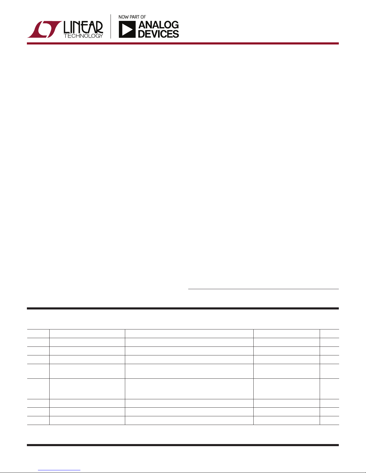
QUICK START PROCEDURE
Refer to Figure 1 for proper measurement equipment
setup and follow the procedure below:
NOTE: When measuring the output voltage during switching transitions, care must be taken to avoid a long ground
lead on the oscilloscope probe. Measure the output voltage by touching the probe tip and ground ring directly
across the output capacitor as shown in Figure 2.
1. Place SW1 to OFF position. Move JP1 from the PULSE
(default position) to ON/OFF position (load on continu
ously when SW1 is ON).
2. With input power supply set to zero volts and power
off, connect the input power supply to +VIN and GND.
3. With power off, connect load from +VOUT to GND.
4. Turn on the input power supply and increase the input
voltage slowly to 9V minimum. The input range is up
to 135V but hot-plugging with long leads may result
in input voltages in excess of 135V.
-
5. Place SW1 to ON position.
6. Check for the proper output voltage using a voltmeter.
Output voltage should be close to input voltage.
NOTE: If there is no output, temporarily disconnect the
load and cycle SW1 (the ON/OFF switch) or press reset
pushbutton SW2. If output is good, the load may be
set too high.
7. Once the proper output voltage is established, adjust
the load, if desired, to test current limit.
8. Placing SW1 to OFF position, moving JP1 to PULSE
position then placing SW1 in ON position will allow
pulse operation. Pushing SW2 will turn the high side
on for 300µs time.
switch
9. Placing SW1 to OFF position, moving JP1 to INPUT
position connects INPUT terminal to LTC7000 INP pin.
An INPUT pin voltage of 2.2V or more will turn-on the
high side switch.
2
Figure 1. Proper Measurement Equipment Setup
dc2537af
Page 3
QUICK START PROCEDURE
50V/DIV
DEMO MANUAL DC2537A
+ –
V
Figure 2. Measuring Output Voltage During Switching across C9. Note that C9 May Not Be Installed
OUT
C9
GND
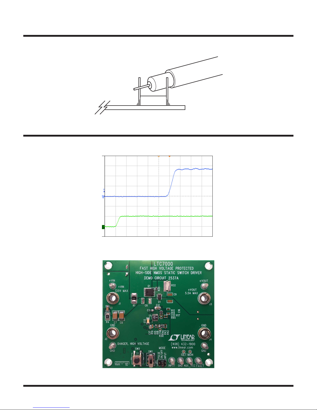
TYPICAL PERFORMANCE CHARATERISTICS
Figure 3. Rise Time into 50Ω Load (V
= 135V, CH4 V
IN
INP
5V/DIV, CH3 V
V
OUT
V
INP
5V/DIV
20V/DIV, 10ns/DIV)
OUT
Figure 4. Board Photo
dc2537af
3
Page 4

DEMO MANUAL DC2537A
PARTS LIST
ITEM QTY REFERENCE PART DESCRIPTION MANUFACTURER/PART NUMBER
Required Circuit Components
1 5 C3, C4, C5, C7, C8 CAP., 1µF, X7T, 250V, 1812 TDK, C4532X7T2E105K250KA
2 2 C11, C14 CAP., 1000pF, X7R, 25V, 10%, 0603 MURATA, GRM188R71E102KA01D
3 1 C12 CAP., 0.1µF, X7R, 25V, 10%, 0805 AVX, 08053C104KAT2A
4 1 C13 CAP., 0.1µF, X7R, 200V, 10%, 1206 AVX, 12062C104KAT2A
5 1 C17 CAP., 1µF, X7R, 25V, 10%, 0805 AVX, 08053C105KAT2A
6 1 D1 DIODE, ES1PD, 200V, 1A, DO-220AA VISHAY, ES1PD-M3/84A
7 1 Q1 MOSFET, N-CH, 150V, POWERPAK-SO-8 FAIRCHILD, FDMS86250
8 1 R1 RES., SENSE, 0.004Ω, 1W, 2%, 2512 PANASONIC, ERJM1WTF4M0U
9 2 R7 RES., 100Ω, 1/10W, 1%, 0603 VISHAY, CRCW0603100RFKEA
10 2 R15, R46 RES., 100k, 1/10W, 1%, 0603 VISHAY CRCW0603100KFKEA
11 1 R35 RES., 10Ω, 1/10W, 1%, 0603 VISHAY, CRCW060310R0FKEA
12 1 R40 RES., 1M, 1/10W, 1%, 0805 VISHAY, CRCW08051M00FKEA
13 1 U1 IC, LTC7000EMSE, MSE-16 LINEAR TECH., LTC7000EMSE#PBF
Additional Demo Board Circuit Components
14 1 C1 CAP., 10nF, X7R, 200V, 10%, 1206 AVX, 12062C103KAZ2A
15 1 C2 CAP., 22µF, ALUM, 160V, 20%, TH C-10X12.5 SUN ELECT., 160ME22HPC
16 1 R4 RES., 100Ω, 1/2W, 5%, 1210 NIC, NRCP25J101TRF
17 0 C6, C9 CAP., OPTIONAL, 1812 OPTIONAL
18 0 C10 CAP., OPTIONAL, TH C-10X12 OPTIONAL
19 0 C16 CAP., OPTIONAL, 1206 OPTIONAL
20 2 C18, C19 CAP., 0.1µF, X7R, 25V, 10%, 0603 AVX, 06033C104KAT2A
21 0 C21, C22, C23 CAP., OPTIONAL, 0603 OPTIONAL
22 0 D2, D3, D4 DIODE, OPTIONAL, SOT23 OPTIONAL
23 1 D5 DIODE, MMSZ5V1T1, SOD-123 ON SEMICONDUCTOR, MMSZ5V1T1G
24 1 D6 DIODE, MMBD4148, SOT23 DIODES INC., MMBD4148-7-F
25 0 D7 DIODE OPTION, PDS4150, POWERDI5 OPTIONAL
26 0 D8 DIODE, OPTION, BAS21, SOT23 OPTIONAL
27 0 D9 DIODE., OPTION, CMMR1U, SOD-123F OPTIONAL
28 0 Q2 MOSFET, N-CH, 80V, PSOF08A FAIRCHILD, FDBL86361_F085
29 0 Q3 MOSFET, OPTIONAL, POWERPAK-SO-8 OPTIONAL
30 1 Q4 XSTR, PNP, 0.2A, MMBT3906, SOT23 FAIRCHILD, MMBT3906
31 1 Q5 MOSFET, P-CH, –200V, SOT23 DIODES INC., ZXMP2120FFTA
32 1 R2 RES., 0Ω, 1/10W, 1%, 0805 VISHAY CRCW08050000Z0EA
33 9 R6, R12, R14, R22, R25, R43, R45, R47 RES., 0Ω, 1/10W, 0603 VISHAY CRCW06030000Z0EA
34 0 R9, R17, R41, R42 RES., OPTIONAL, 0805 OPTIONAL
4
dc2537af
Page 5

DEMO MANUAL DC2537A
PARTS LIST
ITEM QTY REFERENCE PART DESCRIPTION MANUFACTURER/PART NUMBER
35 0 R13, R18, R19, R33, R34, R36, R39, R44 RES., OPTIONAL, 0603 OPTIONAL
36 3 R21, R37, R38 RES., 100k, 1/10W, 1%, 0603 VISHAY CRCW0603100KFKEA
37 1 R23 RES., 787Ω, 1/10W, 1%, 0603 VISHAY, CRCW0603787RFKEA
38 2 R27, R31 RES., 240k, 1/10W, 1%, 0805 VISHAY CRCW0805240KFKEA
39 1 R28 RES., 976k, 1/10W, 1%, 0603 VISHAY CRCW0603976KFKEA
40 1 R29 RES., 232k, 1/10W, 1%, 0603 VISHAY CRCW0603232KFKEA
41 1 R30 RES., 182k, 1/10W, 1%, 0603 VISHAY CRCW0603182KFKEA
42 1 R32 RES., SENSE, 0Ω, 1/2W, 1%, 1225 TEPRO, RN5326
43 1 SW1 SWITCH, SUB MINIATURE SLIDE C&K COMPONENTS, JS202011CQN
44 1 SW2 SWITCH, MICRO MINIATURE PUSHBUTTON TE CONNECTIVITY, FSM4JSMA
45 1 U2 IC, LTC6993CS6-3, TSOT23-6 LINEAR TECH., LTC6993CS6-3#PBF
Hardware: For Demo Board Only
46 8 E1-E8 TESTPOINT, TURRET 0.094" MILL MAX 2501-2-00-80-00-00-07-0
47 1 JP1 CONN., HEADER, 2X3, 2mm WURTH ELEKTRONIK, 62000621121
48 4 J1, J2, J3, J4 CONN, BANANA JACK KEYSTONE 575-4
49 1 XJP1 SHUNT, 2MM WURTH ELEKTRONIK, 60800213421
50 4 MTGS. AT 4 CORNERS STAND-OFF, NYLON 0.559" tall WURTH ELEKTRONIK, 702935500
dc2537af
5
Page 6

DEMO MANUAL DC2537A
5
4
3
2
1
12
12
12
SCHEMATIC DIAGRAM
3
3
3
www.linear.com
www.linear.com
KURK M.
www.linear.com
KURK M.
KURK M.
+VOUT
+VOUT
5.5A MAX
E3
J3
PRODUCTION3 08-16-17
PRODUCTION3 08-16-17
PRODUCTION3 08-16-17
REVISION HISTORY
DESCRIPTION DATEAPPROVEDECO REV
REVISION HISTORY
DESCRIPTION DATEAPPROVEDECO REV
REVISION HISTORY
DESCRIPTION DATEAPPROVEDECO REV
+VOUT
__
__
__
3
Q1
FDMS86250
2
678
R32
C9
OPT
1812
D1
0
1225
1
5
R35
10
4
TD TS
100
R7
R1
0.004
2512
R42
1W
OPT
2%
0805
0
R6
R43
ES1PD
C12
BST
C11
0
GND
E4
0.1uF
14
15
1nF
16
8
R41
GND
J4
TG
R12
1206-0805
BST
SNS-
C21
OPT
OPT
0805
12
SNS+
OVLO
1
0
TGUP
U1
RUN
VIN2
D4
R14
0
11
13
TS
TGDN
LTC7000EMSE
FAULT
VIN
2
5
BST
R47
VCC
3
10
VCC
IMON
0
OPT
4
VCCUV
ISET
9
C23
OPT
TIMER
GND
INP
R44
R17
6
7
OPT
Fax: (408)434-0507
Milpitas, CA 95035
Phone: (408)432-1900
1630 McCarthy Blvd.
LTC Confidential-For Customer Use Only
Fax: (408)434-0507
Milpitas, CA 95035
Phone: (408)432-1900
1630 McCarthy Blvd.
LTC Confidential-For Customer Use Only
Fax: (408)434-0507
Milpitas, CA 95035
Phone: (408)432-1900
1630 McCarthy Blvd.
LTC Confidential-For Customer Use Only
TECHNOLOGY
TECHNOLOGY
TECHNOLOGY
FAST HIGH VOLTAGE PROTECTED HIGH-SIDE
SCHEMATIC
SCHEMATIC
SCHEMATIC
C17
1uF
0805
200V
OPT
1206
C16
OPT
0805
OPT
R19
100K
R46
16V
C14
1nF
Vccuv rising = 7.0V typ (7.5V max)
R18
OPT
VCC
17
Vccuv falling = 6.4V typ (5.8V min)
OPT
R39
TITLE:
TITLE:
TITLE:
KURK M.
LT
KURK M.
LT
KURK M.
LT
APPROVALS
APPROVALS
APPROVALS
PCB DES.
PCB DES.
PCB DES.
APP ENG.
APP ENG.
APP ENG.
CUSTOMER NOTICE
CUSTOMER NOTICE
CUSTOMER NOTICE
LINEAR TECHNOLOGY HAS MADE A BEST EFFORT TO DESIGN A
CIRCUIT THAT MEETS CUSTOMER-SUPPLIED SPECIFICATIONS;
HOWEVER, IT REMAINS THE CUSTOMER'S RESPONSIBILITY TO
VERIFY PROPER AND RELIABLE OPERATION IN THE ACTUAL
APPLICATION. COMPONENT SUBSTITUTION AND PRINTED
CIRCUIT BOARD LAYOUT MAY SIGNIFICANTLY AFFECT CIRCUIT
PERFORMANCE OR RELIABILITY. CONTACT LINEAR
SHEET OF
SHEET OF
SHEET OF
1
DC2537A
DC2537A
DC2537A
LTC7000EMSE
LTC7000EMSE
LTC7000EMSE
NMOS STATIC SWITCH DRIVER
Wednesday, August 16, 2017
Wednesday, August 16, 2017
Wednesday, August 16, 2017
IC NO. REV.
IC NO. REV.
IC NO. REV.
N/A
N/A
N/A
SIZE
DATE:
SIZE
DATE:
SIZE
DATE:
2
SCALE = NONE
SCALE = NONE
SCALE = NONE
3
TECHNOLOGY APPLICATIONS ENGINEERING FOR ASSISTANCE.
THIS CIRCUIT IS PROPRIETARY TO LINEAR TECHNOLOGY AND
SUPPLIED FOR USE WITH LINEAR TECHNOLOGY PARTS.
TECHNOLOGY APPLICATIONS ENGINEERING FOR ASSISTANCE.
THIS CIRCUIT IS PROPRIETARY TO LINEAR TECHNOLOGY AND
SUPPLIED FOR USE WITH LINEAR TECHNOLOGY PARTS.
TECHNOLOGY APPLICATIONS ENGINEERING FOR ASSISTANCE.
THIS CIRCUIT IS PROPRIETARY TO LINEAR TECHNOLOGY AND
SUPPLIED FOR USE WITH LINEAR TECHNOLOGY PARTS.
250V
1812
250V
1812
250V
1812
160V
R4
100
1206
135VIN MAX
1210
R40
5%
R200805
C8
1uF
C7
1uF
C6
OPT
J1
+VIN
VIN
22uF
C2
+
C1
10nF
200V
E1
+VIN
D D
6
GND
1MEG
E2
0805
GND
J2
R15
100k
VCC
E6
P1
DANGER,
C C
FAULT
HIGH VOLTAGE
IMON
C13
0.1uF
1206
200V
C22
OPT
P2
ISET
INPUT
123456
MODE
R45
ON/OFF
0
E7
INPUT
B B
PULSE
R36
JP1
OPT
TRIGOUTONOFF
See Page 2 for SW1 (ON/OFF)
and SW2 (PULSE)
E8
GND
Note: Unless otherwise specified:
All resistors are in ohms, 1%, 0603.
All capacitors are in microfarads 0603.
All capacitors are 25V.
Note: OPT = (OPT) = Optional = Not Used
1/16W = 0402, 1/10W = 0603, 1/8W = 0805,
4
5
1/4W = 1206, 1/2W =1210, 1W = 2512.
1uF 250V TDK C4532X7T2E105K250KA (1812, X7T, -50% at 125V).
22uF 160V Sun Elect Ind 160ME22HPC (10X12.5,153mA at 120Hz).
5.1V Zener On Semi MMSZ5V1T1.
0 Ohm 1225 TEPRO RN5326
0.004ohms 1W Panasonic ERJM1WTF4M0U (2512).
100ohm 1210 NIC NRCP25J101TRF (0.5W, 400W for 0.1ms).
Fairchild FDMS86250 (150V, 25mohmmax and 25nCtyp at 10V, 33mohmmax at 6V, Power56).
A A
dc2537af
Page 7

DEMO MANUAL DC2537A
5
4
3
2
1
22
22
22
SCHEMATIC DIAGRAM
3
3
3
www.linear.com
www.linear.com
www.linear.com
R31
240K
R27
ON
VIN2
OFF
SW1
4 1
5 2
6 3
JS202011CQN
R23
Q4
R25
787
MMBT3906
0
Q5
240K
ZXMP2120FF
5V
1
23
4
SW2
FSM4JSMA
PULSE or RESET
R37
100k
5V
R38
D6
MMBD4148
100k
C19
0.1uF
R22
0
TRIGOUT
U2
LTC6993CS6-3
100K
R21
5V
R28
5
6
V+
OUT
TRG1GND2SET
4
3
0805
0805
C18
D5
5.1V
0.1uF
Milpitas, CA 95035
Phone: (408)432-1900
1630 McCarthy Blvd.
Milpitas, CA 95035
Phone: (408)432-1900
1630 McCarthy Blvd.
Milpitas, CA 95035
Phone: (408)432-1900
1630 McCarthy Blvd.
Fax: (408)434-0507
LTC Confidential-For Customer Use Only
Fax: (408)434-0507
LTC Confidential-For Customer Use Only
Fax: (408)434-0507
LTC Confidential-For Customer Use Only
TECHNOLOGY
TECHNOLOGY
TECHNOLOGY
FAST HIGH VOLTAGE PROTECTED HIGH-SIDE
SCHEMATIC
SCHEMATIC
SCHEMATIC
TITLE:
TITLE:
TITLE:
976k
KURK M.
LT
KURK M.
LT
KURK M.
R30
182k
DIV
LT
APPROVALS
APPROVALS
APPROVALS
PCB DES.
PCB DES.
PCB DES.
APP ENG.
APP ENG.
APP ENG.
T=300us
232k
R29
ONOFF
SHEET OF
SHEET OF
SHEET OF
1
DC2537A
DC2537A
DC2537A
LTC7000EMSE
LTC7000EMSE
LTC7000EMSE
NMOS STATIC SWITCH DRIVER
Wednesday, August 16, 2017
Wednesday, August 16, 2017
Wednesday, August 16, 2017
IC NO. REV.
IC NO. REV.
IC NO. REV.
N/A
N/A
N/A
SIZE
DATE:
SIZE
DATE:
SIZE
DATE:
2
SCALE = NONE
SCALE = NONE
SCALE = NONE
OPTIONAL ON/OFF
and SINGLE SHOT
CUSTOMER NOTICE
CUSTOMER NOTICE
CUSTOMER NOTICE
LINEAR TECHNOLOGY HAS MADE A BEST EFFORT TO DESIGN A
CIRCUIT THAT MEETS CUSTOMER-SUPPLIED SPECIFICATIONS;
HOWEVER, IT REMAINS THE CUSTOMER'S RESPONSIBILITY TO
VERIFY PROPER AND RELIABLE OPERATION IN THE ACTUAL
APPLICATION. COMPONENT SUBSTITUTION AND PRINTED
CIRCUIT BOARD LAYOUT MAY SIGNIFICANTLY AFFECT CIRCUIT
PERFORMANCE OR RELIABILITY. CONTACT LINEAR
LINEAR TECHNOLOGY HAS MADE A BEST EFFORT TO DESIGN A
LINEAR TECHNOLOGY HAS MADE A BEST EFFORT TO DESIGN A
160V
C10
OPT
+
+VOUT
5
678
D7
OPT
PowerDI5
3
12
Q3
C5
250V
1uF
1812
C4
250V
1uF
1812
OPT POWERPAK-SO-8
Q2
C3
250V
1uF
1812
OPT PSOF08
VIN
4
2
3
1
TS
SD
OPT
R34
D3
TG
TG TS
R33
OPT
G
D2
VCC
21
D9
OPT (CMPZ5242B)
VIN2VIN
D8
OPT
OPT
OPT
SOT23
SOD-123F
R9
OPT
R13
0805
OPT
BST
TD
E5
TECHNOLOGY APPLICATIONS ENGINEERING FOR ASSISTANCE.
CIRCUIT THAT MEETS CUSTOMER-SUPPLIED SPECIFICATIONS;
HOWEVER, IT REMAINS THE CUSTOMER'S RESPONSIBILITY TO
VERIFY PROPER AND RELIABLE OPERATION IN THE ACTUAL
APPLICATION. COMPONENT SUBSTITUTION AND PRINTED
CIRCUIT BOARD LAYOUT MAY SIGNIFICANTLY AFFECT CIRCUIT
PERFORMANCE OR RELIABILITY. CONTACT LINEAR
TECHNOLOGY APPLICATIONS ENGINEERING FOR ASSISTANCE.
3
THIS CIRCUIT IS PROPRIETARY TO LINEAR TECHNOLOGY AND
SUPPLIED FOR USE WITH LINEAR TECHNOLOGY PARTS.
THIS CIRCUIT IS PROPRIETARY TO LINEAR TECHNOLOGY AND
SUPPLIED FOR USE WITH LINEAR TECHNOLOGY PARTS.
THIS CIRCUIT IS PROPRIETARY TO LINEAR TECHNOLOGY AND
SUPPLIED FOR USE WITH LINEAR TECHNOLOGY PARTS.
4
5
AUX_VCC
D D
C C
B B
A A
dc2537af
Information furnished by Linear Technology Corporation is believed to be accurate and reliable.
However, no responsibility is assumed for its use. Linear Technology Corporation makes no representation that the interconnection of its circuits as described herein will not infringe on existing patent rights.
7
Page 8

DEMO MANUAL DC2537A
DEMONSTRATION BOARD IMPORTANT NOTICE
Linear Technology Corporation (LTC) provides the enclosed product(s) under the following AS IS conditions:
This demonstration board (DEMO BOARD) kit being sold or provided by Linear Technology is intended for use for ENGINEERING DEVELOPMENT
OR EVALUATION PURPOSES ONLY and is not provided by LTC for commercial use. As such, the DEMO BOARD herein may not be complete
in terms of required design-, marketing-, and/or manufacturing-related protective considerations, including but not limited to product safety
measures typically found in finished commercial goods. As a prototype, this product does not fall within the scope of the European Union
directive on electromagnetic compatibility and therefore may or may not meet the technical requirements of the directive, or other regulations.
If this evaluation kit does not meet the specifications recited in the DEMO BOARD manual the kit may be returned within 30 days from the date
of delivery for a full refund. THE FOREGOING WARRANTY IS THE EXCLUSIVE WARRANTY MADE BY THE SELLER TO BUYER AND IS IN LIEU
OF ALL OTHER WARRANTIES, EXPRESSED, IMPLIED, OR STATUTORY, INCLUDING ANY WARRANTY OF MERCHANTABILITY OR FITNESS
FOR ANY PARTICULAR PURPOSE. EXCEPT TO THE EXTENT OF THIS INDEMNITY, NEITHER PARTY SHALL BE LIABLE TO THE OTHER FOR
ANY INDIRECT, SPECIAL, INCIDENTAL, OR CONSEQUENTIAL DAMAGES.
The user assumes all responsibility and liability for proper and safe handling of the goods. Further, the user releases LTC from all claims
arising from the handling or use of the goods. Due to the open construction of the product, it is the user’s responsibility to take any and all
appropriate precautions with regard to electrostatic discharge. Also be aware that the products herein may not be regulatory compliant or
agency certified (FCC, UL, CE, etc.).
No License is granted under any patent right or other intellectual property whatsoever. LTC assumes no liability for applications assistance,
customer product design, software performance, or infringement of patents or any other intellectual property rights of any kind.
LTC currently services a variety of customers for products around the world, and therefore this transaction is not exclusive.
Please read the DEMO BOARD manual prior to handling the product. Persons handling this product must have electronics training and
observe good laboratory practice standards. Common sense is encouraged.
This notice contains important safety information about temperatures and voltages. For further safety concerns, please contact a LTC application
engineer.
Mailing Address:
Linear Technology
1630 McCarthy Blvd.
Milpitas, CA 95035
Copyright © 2004, Linear Technology Corporation
8
dc2537af
LT 0917 • PRINTED IN USA
LINEAR TECHNOLOGY CORPORATION 2017
 Loading...