

Linear LTC6602, LTC6603 Quick Start Manual
D E M O C IRC U IT
D E M O C IRC U IT D E M O C IRC U IT
D E M O C IRC U IT
1 3 0 4
1 3 0 41 3 0 4
1 3 0 4
LT C 6 6 0 2 / L T C 6 6 0 3
P RO G RA M A B L E B A N D P A S S / L O W P A S S F IL T E R
D E S C R IP T IO N
Demonstration Circuit 1304A features tw o programmable
filter ICs, the LTC6602 dual, matched, bandpass filter and
the LTC6603, dual, matched, low pass filter.
The DC1304A
The DC1304A----AAAA is for
The DC1304AThe DC1304A
The DC1304A
The DC1304A----B is for
The DC1304AThe DC1304A
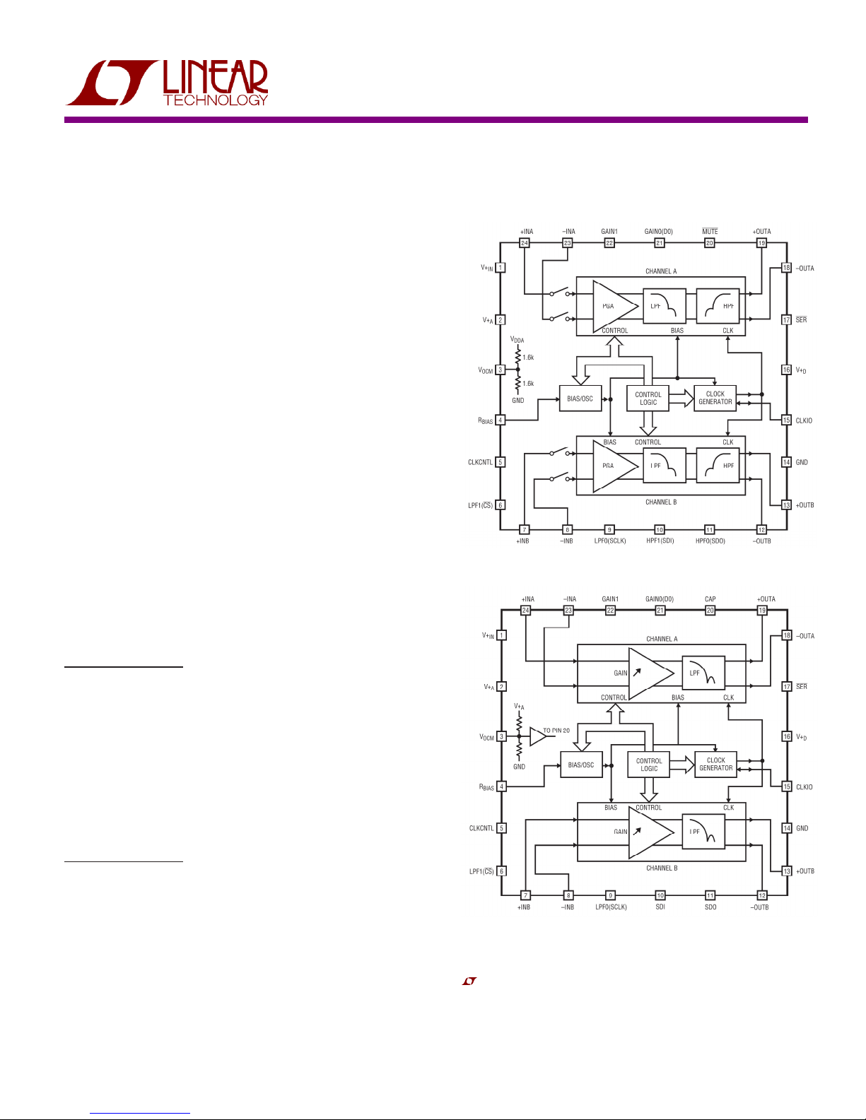
The LTC® 6602 is a dual, programmable bandpass filter
and differential driver. The selectivity of the LTC6602 is
ideal for filtering baseband tag signals in RFID systems.
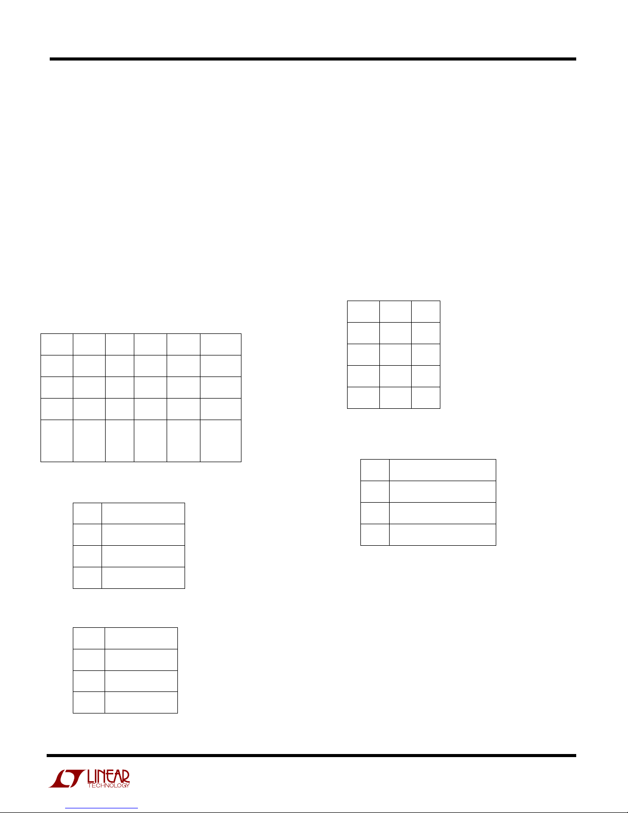
The LTC® 6603 is a dual, programmable low pass filter for
communications receivers and transmitters in TD-SCDM A,
W CDM A, CDM A2000, U M TS and 802.11x systems. A
DC1304A-A or ---B board has tw o pairs of SM A connectors
for differential inputs and tw o pairs of SM A connectors for
differential outputs. The differential inputs can be AC coupled or DC coupled. O n board jumpers provide control of an
LTC6602 or an LTC6603. The jumper control settings are:
serial or parallel control, internal or external clock, gain and
bandw idth control and input AC or DC coupling. An on
board multi-turn potentiometer sets the value of the R BIAS
resistor that sets the IC pow er supply current and clock
frequency. PCB turrets provide for board connections to an
SPI master for a serial control of IC gain and bandw idth.
LTC6602 features:
LTC6602 features:
LTC6602 features:LTC6602 features:
Guaranteed Phase and G ain M atching Specs
Programmable 5th O rder Low pass: 40 kH z to 900 kHz
Programmable 4th O rder H ighpass: 4 kH z to 90 kH z
Programmable G ain (0dB/12dB/24dB/30dB)
Simple Pin Programming or SPI Interface
Input Range Extends from 0V to 5V
Low Voltage O peration: 2.7V to 3.6V
Shutdow n and M ute M ode
4mm × 4mm Q FN Package
LTC6603 features:
LTC6603 features:
LTC6603 features:LTC6603 features:
Guaranteed Phase and G ain M atching Specs
Programmable 9th O rder Low pass: 24 kH z to 2.5 M Hz
Programmable G ain (0dB/6dB/12dB/24dB)
Simple Pin Programming or SPI Interface
Input Range Extends from 0V to 5V
Low Voltage O peration: 2.7V to 3.6V
Shutdow n M ode
4mm × 4mm Q FN Package
is for an LTC6602 and
an LTC6602 and
is for is for
an LTC6602 and an LTC6602 and
B is for an LTC6603.
B is forB is for
an LTC6603.
an LTC6603. an LTC6603.
T h e L T C 6 6 0 2 B L O C K D IA G
T h e L T C 6 6 0 2 B L O C K D IA G RRRRA RA M
T h e L T C 6 6 0 2 B L O C K D IA GT h e L T C 6 6 0 2 B L O C K D IA G
A RA M
A RA MA RA M
T h e L T C 6 6 0 3 B L O C K D IA
T h e L T C 6 6 0 3 B L O C K D IA RRRRG A RA M
T h e L T C 6 6 0 3 B L O C K D IAT h e L T C 6 6 0 3 B L O C K D IA
G A RA M
G A RA MG A RA M
Design Files for this circuit are available.
Design Files for this circuit are available.
Design Files for this circuit are available.Design Files for this circuit are available.
Call the LTC factory.
Call the LTC factory.
Call the LTC factory.Call the LTC factory.
, LTC and LT are registered trademarks of Linear Technology Corporation.

DC1304 QUICK START GUIDE
Q U ICK TEST SETU P
Q U ICK TEST SETU P –––– PAR ALLEL CO NTR O L
Q U ICK TEST SETU PQ U ICK TEST SETU P
PAR ALLEL CO N TR O L
PAR ALLEL CO N TR O L PAR ALLEL CO N TR O L
Q U IC K T E S T P R O C E D U R E
Test P roc
Test P roceeeedure
Test P rocTest P roc
dure
duredure
1. Connect DC1304 as show n, turn on pow er and adjust
the RBIAS1 pot for 50M H z.
2. Connect 50 ohm terminator to AIN -(J2) and sinewave
generator to AIN+ (J1).
3. Connect oscilloscope to VO UTA+ and on the oscillo-
scope display must show a 1Vp-p sinew ave.
4. Connect oscilloscope to VO UTA- and on the oscillo-
scope display must show a 1Vp-p sinew ave.
5. Connect 50 ohm terminator to BIN-(J2) and sinew ave
generator to BIN + (J1).
6. Connect oscilloscope to VO UTB+ and on the oscillo-
scope display must show a 1Vp-p sinew ave.
7. Connect oscilloscope to VO UTB- and on the oscillo-
scope display must show a 1Vp-p sinew ave.
2
DC1304 QUICK START GUIDE
LTC6602 FCLK AN D FCU TO FF RAN G E
LTC6602 FCLK AN D FCU TO FF RAN G E
LTC6602 FCLK AN D FCU TO FF RAN G ELTC6602 FCLK AN D FCU TO FF RAN G E
FCLK R ange, 24M H z to 90M H z
FCLK R ange, 24M H z to 90M H z
FCLK R ange, 24M H z to 90M H zFCLK R ange, 24M H z to 90M H z
RBIAS = (4.941 10^9) / FCLK; RBIAS in k
Example: If FCLK = 50 M Hz Then
RBIAS = (4.941 10^9) / (50 10^6) = 98.82k
The Lowpass FCUTO FF = FCLK / NLP
The Highpass FCU TO FF = FCLK / N HP
NLP and NH P are the clock dividers set by the
(LPF1, LPF0) and (HPF1, H PF0) inputs respectively.
LPF1 LPF0 NLP HPF1 H PF0 N HP
0 0 600 0 0 6000
0 1 300 0 1 2000
1 0 100 1 0 1000
LTC6602 FCLK AN D FCU TO FF RAN G E
LTC6602 FCLK AN D FCU TO FF RAN G E
LTC6602 FCLK AN D FCU TO FF RAN G ELTC6602 FCLK AN D FCU TO FF RAN G E
FCLK R ange, 12M H z to 80M H z
FCLK R ange, 12M H z to 80M H z
FCLK R ange, 12M H z to 80M H zFCLK R ange, 12M H z to 80M H z
RBIAS = (2.472 10^9) / FCLK; RBIAS in k
Example: If FCLK = 50 M Hz Then
RBIAS = (2.472 10^9) / (50 10^6) = 49.44k
The Lowpass FCUTO FF = FCLK / NLP
NLP clock divider set by the (LPF1, LPF0) inputs.
LPF1 LPF0 NLP
0 0 512
0 1 128
1 0 32
1 1 32
1 1 100 1 1 Bypass
HPF
Low pass Filter FCU TOFF
Low pass Filter FCU TO FF R ange
Low pass Filter FCU TO FFLow pass Filter FCU TO FF
R ange
R ange R ange
NLP Range
100 240kHz – 900kH z
300 80kHz – 300kH z
600 40kHz – 150kH z
H ighpass Filter FCU TOFF
H ighpass Filter FCU TOFF R ange
H ighpass Filter FCU TOFFH ighpass Filter FCU TOFF
R ange
R ange R ange
NH P Range
1000 24kH z – 90kHz
2000 12kH z – 45kHz
6000 4kH z – 15kHz
Low pass Filter
Low pass Filter FCU TO FF R ange
Low pass Filter Low pass Filter
FCU TO FF Range
FCU TO FF RangeFCU TO FF Range
NLP Range
32 375kHz – 2.5M Hz
128 93.75kHz – 625kHz
512 23.44kHz – 156.25kHz
3
 Loading...