


LTC4413-1/LTC4413-2
Dual 2.6A, 2.5V to 5.5V
Fast Ideal Diodes
in 3mm × 3mm DFN
FEATURES
n
2-Channel Ideal Diode OR’ing or Load Sharing
n
Low Loss Replacement for PowerPath™ OR’ing
Diodes
n
Fast Response Replacement for LTC4413
n
Low Forward On-Resistance (140mΩ Max at 3.6V)
n
Low Reverse Leakage Current
n
Low Regulated Forward Voltage (18mV Typ)
n
Overvoltage Protection Sensor with Drive Output for
an External P-Channel MOSFET (LTC4413-2 Only)
n
2.5V to 5.5V Operating Range
n
2.6A Maximum Forward Current
n
Internal Current Limit Protection
n
Internal Thermal Protection
n
Status Output to Indicate if Selected Channel is
Conducting
n
Programmable Channel On/Off
n
Low Profi le (0.75mm) 10-Lead 3mm × 3mm DFN
Package
APPLICATIONS
n
Battery and Wall Adapter Diode OR’ing in Handheld
Products
n
Backup Battery Diode OR’ing
n
Power Switching
n
USB Peripherals
n
Uninterruptable Supplies
DESCRIPTION
The LTC®4413-1 and LTC4413-2 each contain two monolithic ideal diodes, each capable of supplying up to 2.6A
from input voltages between 2.5V and 5.5V. The ideal
diodes use a 100mΩ P-channel MOSFET to independently
connect INA to OUTA and INB to OUTB. During normal
forward operation, the voltage drops across each of
these diodes are regulated to as low as 18mV. Quiescent
current is less than 80μA for diode currents up to 1A. If
either of the output voltages exceeds its respective input
voltage, that MOSFET is turned off and less than 1μA of
reverse current fl ows from OUT to IN. Maximum forward
current in each MOSFET is limited to a constant 2.6A and
internal thermal limiting circuits protect the part during
fault conditions. An internal overvoltage protection sensor
detects when a voltage exceeds the LTC4413-2 absolute
maximum voltage tolerance.
Two active-high control pins independently turn off the two
ideal diodes contained within the LTC4413-1/LTC4413-2.
When the selected channel is reverse biased, or the
LTC4413-1/LTC4413-2 is put into low power standby, the
status signal is pulled low by an 11μA open drain.
The LTC4413-1/LTC4413-2 are housed in a 10-lead 3mm
× 3mm DFN package.
L, LT, LTC, LTM, Linear Technology and the Linear logo are registered trademarks of Linear
Technology Corporation. PowerPath is a trademark of Linear Technology Corporation.
All other trademarks are the property of their respective owners.
TYPICAL APPLICATION
Automatic Switchover from a Battery to a Wall Adapter
FDR8508
WALL
ADAPTER
INPUT
INA
0.1μF
1Ω
10μF
ENBA
GND
BAT
+
STAT IS HIGH WHEN WALL ADAPTER IS
SUPPLYING LOAD CURRENT
OVP IS HIGH WHEN WALL ADAPTER VOLTAGE > 6V
ENBB
INB
IDEAL
LTC4413-2
IDEAL
OUTA
STAT
OVI
OVP
OUTB
V
CC
441312 TA01a
470k
4.7μF
STAT
OVP
TO LOAD
Power Loss vs Load
700
600
500
400
300
1N5817
POWER LOSS (mW)
200
100
0
0
500 1000
LTC4413-1
2000 3000
1500 2500
LOAD (mA)
441312 TA01b
441312fd
1

LTC4413-1/LTC4413-2
(
(
ABSOLUTE MAXIMUM RATINGS
INA, INB, OUTA, OUTB, STAT,
ENBA, ENBB Voltage .................................... –0.3V to 6V
OVI, OVP Voltage ....................................... –0.3V to 13V
(Note 1)
Storage Temperature Range ..................–65°C to 125°C
Continuous Power Dissipation ..........................1500mW
(Derate 25mW/°C Above 70°C)
Operating Temperature Range .................–40°C to 85°C
PIN CONFIGURATION
LTC4413-1 LTC4413-2
TOP VIEW
10
INA
1
ENBA
2
11
3
GND
4
ENBB
5
INB
DD PACKAGE
3mm × 3mm) PLASTIC DFN
10-LEAD
T
= 125°C, θJA = 43°C/W
EXPOSED PAD (PIN 11) IS GND, MUST BE SOLDERED TO PCB
JMAX
OUTA
9
STAT
NC
8
7
NC
6
OUTB
TOP VIEW
10
INA
1
ENBA
2
11
3
GND
4
ENBB
5
INB
DD PACKAGE
3mm × 3mm) PLASTIC DFN
10-LEAD
T
= 125°C, θJA = 43°C/W
EXPOSED PAD (PIN 11) IS GND, MUST BE SOLDERED TO PCB
JMAX
OUTA
9
STAT
OVI
8
7
OVP
6
OUTB
ORDER INFORMATION
LEAD FREE FINISH TAPE AND REEL PART MARKING PACKAGE DESCRIPTION TEMPERATURE RANGE
LTC4413EDD-1#PBF LTC4413EDD-1#TRPBF LCPP
LTC4413EDD-2#PBF LTC4413EDD-2#TRPBF LCPQ
10-Lead (3mm × 3mm) Plastic DFN
10-Lead (3mm × 3mm) Plastic DFN
LEAD BASED FINISH TAPE AND REEL PART MARKING PACKAGE DESCRIPTION TEMPERATURE RANGE
LTC4413EDD-1 LTC4413EDD-1#TR LCPP
LTC4413EDD-2 LTC4413EDD-2#TR LCPQ
10-Lead (3mm × 3mm) Plastic DFN
10-Lead (3mm × 3mm) Plastic DFN
Consult LTC Marketing for parts specifi ed with wider operating temperature ranges.
For more information on lead free part marking, go to: http://www.linear.com/leadfree/
For more information on tape and reel specifi cations, go to: http://www.linear.com/tapeandreel/
ELECTRICAL CHARACTERISTICS
The l denotes the specifi cations which apply over the full operating
temperature range, otherwise specifi cations are at TA = 25°C. (Notes 2, 6)
SYMBOL PARAMETER CONDITIONS MIN TYP MAX UNITS
, V
V
IN
Operating Supply Range for Channel A or B VIN and/or V
OUT
Proper Operation
UVLO UVLO Turn-On Rising Threshold Max (V
UVLO Turn-Off Falling Threshold Max (V
I
QF
I
QRIN
I
QRGND
Quiescent Current in Forward Regulation,
Measured via GND
Current Drawn from or Sourced into IN
When V
is Greater than V
OUT
IN
Quiescent Current While in Reverse
Turn-Off, Measured via GND
V
= 3.6V, I
INA
I
= 0mA (Note 3)
INB
VIN = 3.6V, V
V
= V
INA
V
STAT
INA
INA
INB
= 0V
Must be in This Range for
OUT
, V
, V
, V
, V
= V
OUTB
OUTB
OUTA
)
)
INB
INB
OUTA
, V
, V
INB
OUTA
= 100mA, V
INA
= 5.5V (Note 6)
OUT
= 0V, V
OUTB
= 0V,
= 5.5V,
l
2.5 5.5 V
l
l
1.7 V
l
l
–1 2.5 4.5 μA
–40°C to 85°C
–40°C to 85°C
–40°C to 85°C
–40°C to 85°C
2.45 V
40 58 μA
28 36 μA
441312fd
2

LTC4413-1/LTC4413-2
ELECTRICAL CHARACTERISTICS
The l denotes the specifi cations which apply over the full operating
temperature range, otherwise specifi cations are at T
SYMBOL PARAMETER CONDITIONS MIN TYP MAX UNITS
I
QROUTB
I
QOFF
V
RTO
V
FWD
R
FWD
R
ON
t
ON
t
OFF
Short-Circuit Response
I
OC
I
QOC
STAT Output
I
SOFF
I
SON
t
S(ON)
t
S(OFF)
ENB Inputs
V
ENBIH
V
ENBIL
V
ENBHYST
I
ENB
OVI Input (LTC4413-2 Only)
V
OVIH
V
OVIL
V
OVID
I
OVI
Quiescent Current While in Reverse
Turn-Off. Current Drawn from V
OUTA
When
OUTB Supplies Chip Power
Quiescent Current with Both ENBA and
ENBB High
Reverse Turn-Off Voltage (V
Forward Voltage Drop (VIN – V
at I
= –1mA
OUT
On-Resistance, R
Regulation
FWD
– VIN)V
OUT
)
OUT
(Measured as ΔV/ΔI)
On-Resistance, RON Regulation
(Measured as V/I at I
= 1A)
IN
PowerPath Turn-On Time VIN = 3.6V, from ENB Falling to I
PowerPath Turn-Off Time VIN = 3.6V, from ENB Rising with IIN = 100mA
Current Limit V
Quiescent Current While in Overcurrent
Operation
STAT Off Current Shut Down
STAT Sink Current VIN > V
STAT Pin Current Turn-On Time VIN = 3.6V, from ENB Falling 1.8 μs
STAT Pin Current Turn-Off Time VIN = 3.6V, from ENB Rising 0.8 μs
ENB Inputs Rising Threshold Voltage V
ENB Inputs Falling Threshold Voltage V
ENB Input Hysteresis V
ENB Inputs Pull-Down Current V
OVI Input Rising Threshold Voltage V
OVI Input Falling Threshold Voltage V
OVI-OVP Voltage Drop V
OVI Bias Current V
= 25°C. (Notes 2, 6)
A
= V
V
INA
V
INA
IN
V
IN
VIN = 3.6V, I
V
IN
= 0V, V
INB
= V
= 3.6V, V
INB
= 3.6V
= 3.6V
OUT
= 3.6V, IIN = 1A (Note 5) 140 200 mΩ
OUTA
ENBA
= 3.6V, V
= V
ENBB
OUTB
= 1V
= 5.5V
= –100mA to –500mA (Note 5) 100 140 mΩ
Ramp
OUT
l
l
l
–5 10 mV
l
3.5 6.5 μA
28 38 μA
18 24 mV
11 μs
Starting
2μs
Falling to 0mA
= 3.6V (Note 5) 1.8 A
INA OR B
V
= 3.6V, I
INA OR B
, V
OUT
Rising
ENB
Falling
ENB
= (V
ENBHYST
< VIN = 3.6V, V
OUT
Rising 5.9 6.2 V
OVI
Falling 5.4 5.6 V
OVI
= 8V, No Load at OVP 100 mV
OVI
= 8V 80 μA
OVI
= 1.8A (Note 5) 100 130 μA
OUT
l
–1 0 1 μA
< VIL, TJ < 135°C, I
CTL
– V
ENBIH
ENB
ENBIL
< V
IL
< I
OUT
)90mV
MAX
l
71115 μA
l
l
400 460 mV
l
234 μA
540 600 mV
Note 1: Stresses beyond those listed under Absolute Maximum Ratings
may cause permanent damage to the device. Exposure to any Absolute
Maximum Rating condition for extended periods may affect device
reliability and lifetime.
Note 2: The LTC4413-1/LTC4413-2 are guaranteed to meet performance
specifi cations from 0°C to 85°C. Specifi cations over the –40°C to 85°C
operating temperature range are assured by design, characterization and
correlation with statistical process controls.
Note 3: Quiescent current increases with diode current: refer to plot of
I
vs I
OUT
.
QF
Note 4: This IC includes overtemperature protection that is intended
to protect the device during momentary overload conditions.
Overtemperature protection will become active at a junction temperature
greater than the maximum operating temperature. Continuous operation
above the specifi ed maximum operating junction temperature may impair
device reliability.
Note 5: Specifi cation is guaranteed by correlation to wafer-level
measurements.
Note 6: Unless otherwise specifi ed, current into a pin is positive and
current out of a pin is negative. All voltages referenced to GND.
441312fd
3
LTC4413-1/LTC4413-2
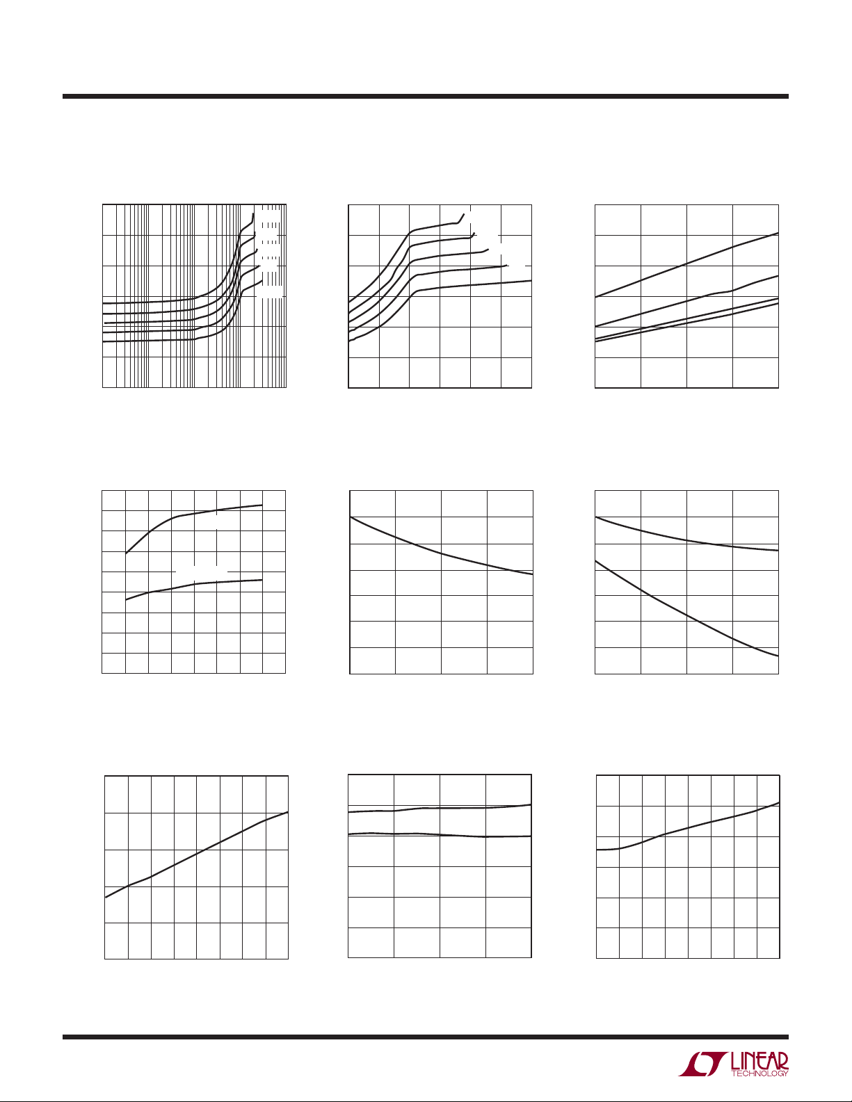
TYPICAL PERFORMANCE CHARACTERISTICS
IQF vs I
120
100
80
(μA)
60
QF
I
40
20
0
1 100 1000 10000
IQF vs V
90
80
70
60
50
(μA)
QF
I
40
30
20
10
0
2.5
2
(Log) IQF vs I
LOAD
10
LOAD (mA)
IN
IQF = 1A
IQF = 100mA
4
VIN (V)
4.5
5
3
3.5
120°C
80°C
40°C
0°C
–40°C
441312 G01
5.5
441312 G04
(Linear) IQF vs Temperature
120
100
(μA)
QF
I
80
60
40
20
0
LOAD
120°C
80°C
40°C
0°C
–40°C
0
1000 1500 2000
500
LOAD (mA)
2500 3000
441312 G02
120
100
(μA)
QF
I
1A
80
60
40
20
0
–40
0 40 80 120
TEMPERATURE (°C)
500mA
100mA
1mA
441312 G03
IOC vs Temperature UVLO Thresholds vs Temperature
3500
3000
2500
2000
(mA)
OC
I
1500
1000
500
6
0
–40
0 40 120
TEMPERATURE (°C)
80
441312 G05
2.20
2.15
2.10
2.05
2.00
1.95
UVLO THRESHOLDS (V)
1.90
1.85
–40
0 40 120
TEMPERATURE (°C)
RISING
FALLING
80
441312 G06
UVLO Hysteresis vs Temperature
250
200
150
100
UVLO HYSTERESIS (mV)
50
0
–40
–20 0
20 60 120
TEMPERATURE (°C)
4
ENB Thresholds vs Temperature ENB Hysteresis vs Temperature
600
500
400
300
200
ENBIH/ENBIL (mV)
100
0
40
80 100
441312 G07
–40
0 40 80 120
TEMPERATURE (°C)
ENBIH
ENBIL
441312 G08
120
100
80
60
40
ENB HYSETERSIS (mV)
20
0
–40
040
–20 20
TEMPERATURE (°C)
80
60
100
441312 G09
441312fd
120

TYPICAL PERFORMANCE CHARACTERISTICS
0
R
FWD
80
78
76
74
72
70
500mA (mΩ)
68
FWD
R
66
64
62
60
2
2.5 3.5
V
FWD
250
200
150
(mV)
FWD
V
100
50
vs VIN and I
3
vs I
120°C
80°C
40°C
0°C
–40°C
LOAD
(Log)
4
VIN (V)
LOAD
4.5
= 500mA
5.5
5
441312 G10
V
and R
FWD
500
400
300
(mΩ)
FWD
R
200
100
0
6
0
120
100
(mΩ)
FWD
R
120°C
80°C
40°C
0°C
–40°C
500
R
FWD
80
60
40
20
vs I
FWD
1000 1500 2000
LOAD
LOAD (mA)
vs Temperature
100mA
1A
(Linear)
V
FWD
R
FWD
2500 3000
441312 G11
500mA
LTC4413-1/LTC4413-2
R
250
200
150
100
50
0
V
FWD
(mV)
600
500
400
(mΩ)
300
FWD
R
200
100
0
1
0.01
(μA)
LEAK
I
0.001
0.0001
FWD
1
0.1
and V
R
FWD
I
LEAK
V
REVERSE
vs I
FWD
10 100 1000 10000
LOAD (mA)
LOAD
120°C
80°C
40°C
0°C
–40°C
V
(Log)
FWD
441312 G12
vs Temperature at
= 5.5V
5.5V
3.6V
300
250
200
150
100
50
0
V
FWD
(mV)
0
1 100 1000 10000
100
10
1
0.1
(μA)
0.01
LEAK
I
0.001
0.0001
0.00001
0
I
LEAK
10
LOAD (mA)
vs V
REVERSE
120°C
80°C
40°C
0°C
–40°C
241356
V
(V)
REVERSE
0
–40
441312 G13
0 40 80 120
TEMPERATURE (°C)
441312 G14
Response to 800mA Load Step
in <16μs
CH1 = IN 100mV/DIV
CH2 OUT
100mV/DIV
CH4 I
OUT
200mV/DIV
4μs/DIV
441312 G16
441312 G17
0.00001
–40 40 80
0–20 60 10020
TEMPERATURE (°C)
ENB Turn-On, 30μs to Turn On
with 180mA Load
CH1 IN 1V/DIV
CH3 ENB
1V/DIV
CH4 I
OUT
200mV/DIV
10μs/DIV
12
441312 G15
CH2 OUT
1V/DIV
441312 G18
441312fd
5

LTC4413-1/LTC4413-2
0
TYPICAL PERFORMANCE CHARACTERISTICS
ENB Turn-Off, 2μs to Disconnect
IN from 180mA Load
CH2 OUT
1V/DIV
CH3 ENB
1V/DIV
4μs/DIV
CH1 IN 1V/DIV
CH4 I
IN
100mV/DIV
441312 G19
Effi ciency vs Load Current Power Loss vs Load Current
100
99
98
97
96
95
94
EFFICIENCY (%)
93
92
91
90
120°C
80°C
40°C
0°C
–40°C
1 100 1000 10000
10
LOAD (mA)
441312 G20
1000
100
10
POWER LOSS (mW)
1
0
120°C
80°C
40°C
0°C
–40°C
1
100 10 1000 1000
LOAD (mA)
441312 G21
Overvoltage Thresholds
vs Temperature (LTC4413-2 Only)
6.4
6.2
6.0
5.8
5.6
OVPIH/OVPIL (V)
5.4
5.2
5.0
–40
OVP RISING
OVP FALLING
0 40 120
TEMPERATURE (°C)
OVI-OVP Voltage Drop
vs OVI Voltage (LTC4413-2 Only)
6
TA = 25°C
5
4
3
OVP (V)
2
1
0
0
24
812
610
OVI (V)
Overvoltage Hysteresis
vs Temperature (LTC4413-2 Only)
400
350
300
250
200
150
OVP HYSTERESIS (mV)
100
50
0
80
441312 G22
–40
0
40
TEMPERATURE (°C)
120
80
441312 G23
IQ OVI vs Temperature
(LTC4413-2 Only)
180
441312 G25
160
140
120
100
OVI (μA)
80
Q
I
60
40
20
0
–40
IQ OVI = 13V
IQ OVI = 6.5V
0
40
TEMPERATURE (°C)
80
120
441312 G26
OVI Current vs Voltage
(LTC4413-2 Only)
140
TA = 25°C
120
100
80
(μA)
OVI
I
60
40
20
0
0
24
OVI-OVP vs Temperature
(LTC4413-2 Only)
160
140
120
100
80
OVI-OVP (mV)
60
40
20
0
–40
–20
0
V
OHOVP
20
TEMPERATURE (°C)
812
610
V
(V)
OVI
V
OHOVP
= 6.5V
40
60
= 13V
441312 G24
80
100
441312 G27
120
6
441312fd
 Loading...