

Page 1
Description
DEMO MANUAL DC607A
LTC3722, LTC4440, LTC3901,
and LT1431
Isolated Full Bridge Converter
Demonstration circuit 607A is an isolated full bridge
converter featuring the LTC3722, LTC4440, LTC3901,
and LT1431. This circuit was designed to demonstrate the
phase-shifted full bridge power supply to generate 12V
at 35A from a typical telecom input voltage range of 36V
to 72V. Isolation voltage is 1500VDC. Fixed zero-voltage
bridge leg transition times with a 48V input. The DC607A
PCB layout includes options to implement adaptive timing.
Design files for this circuit board are available at
http://www.linear.com/demo/DC607A
L, LT, LTC, LTM, Linear Technology and the Linear logo are registered trademarks of Analog
Devices, Inc. All other trademarks are the property of their respective owners.
transition timing was chosen because of the relatively fast
performance summary
SYMBOL PARAMETER CONDITIONS MIN TYP MAX UNITS
V
IN
V
OUT
I
OUT
f
SW
V
OUT(P-P)
I
REG
P
OUT/PIN
P
OUT/PIN
Input Supply Range 36 72 V
Output Voltage 12.0 V
Output Current Range VIN = 48V, 200LFM 0 35 A
Switching (Clock) Frequency 200 kHz
Output Ripple VIN = 48V, I
Output Regulation Line and Load (36V to 72V, 0A to 35A) ±0.08 %
Efficiency VIN = 48V, I
Efficiency VIN = 48V, I
Isolation Basic 1500 VDC
Approximate Size Component Area × Top Component Height 4.3 × 2.9 × 0.4 Inches
Specifications are at TA = 25°C
= 35A (20MHz BW) 140 mV
OUT
= 35A >93.9 %
OUT
= 25A >94.6 %
OUT
P-P
operating principles
The LTC3722 synchronous dual mode phase modulated
full bridge controller is used on the primary and works
together with the LTC3901 secondary side synchronous
driver to provide a synchronous rectified output. When an
input voltage is applied, the LTC3722 begins a controlled
soft-start of the output voltage. As this voltage begins
to rise, the LT1431 programmable reference is quickly
powered up via the output voltage. The LT1431 provides
feedback via opto-coupler ISO1 to set the output voltage
at 12V. The LTC4440 high voltage gate driver is used to
level shift the high side primary MOSFETs gate signals.
The LTC3722 provides precise control of gate signals to
primary MOSFETs and secondary MOSFETs via T3 and
U1 (LTC3901). The
LTC3901 includes a timer and current
sense to limit reverse inductor current.
For large values of input inductance, a 100V, 47µF electro
lytic capacitor can be added across the input terminals to
damp the input filter and provide adequate stability. See
Linear Technology Application Note 19 for a discussion
on input filter stability analysis. A recommended part is
the SUNCON 100ME47AX.
dc607afa
1
Page 2

DEMO MANUAL DC607A
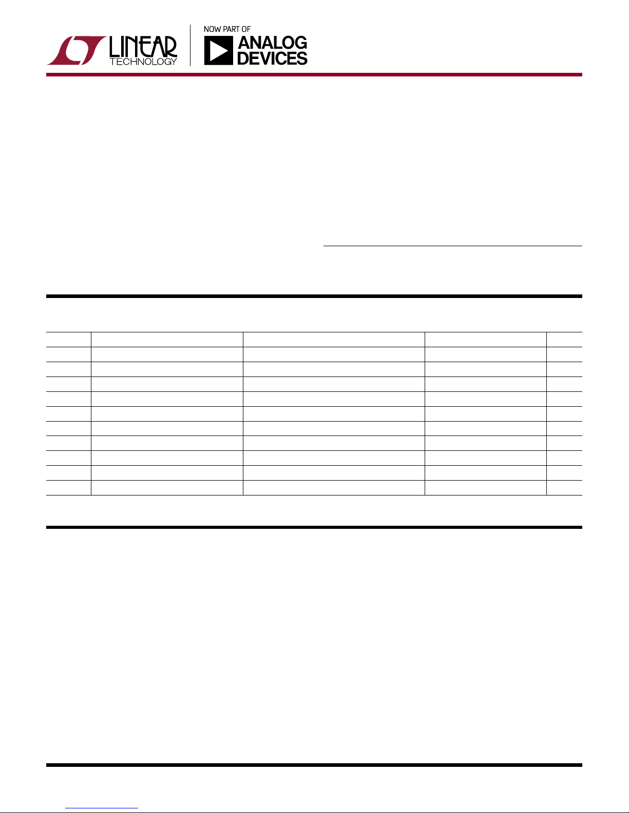
Quick start proceDure
Demonstration circuit 607A is easy to set up to evaluate
the performance of the LTC3722, LTC4440, LTC3901,
and LT1431. Refer to Figure 1 for proper measurement
equipment setup and follow the procedure below:
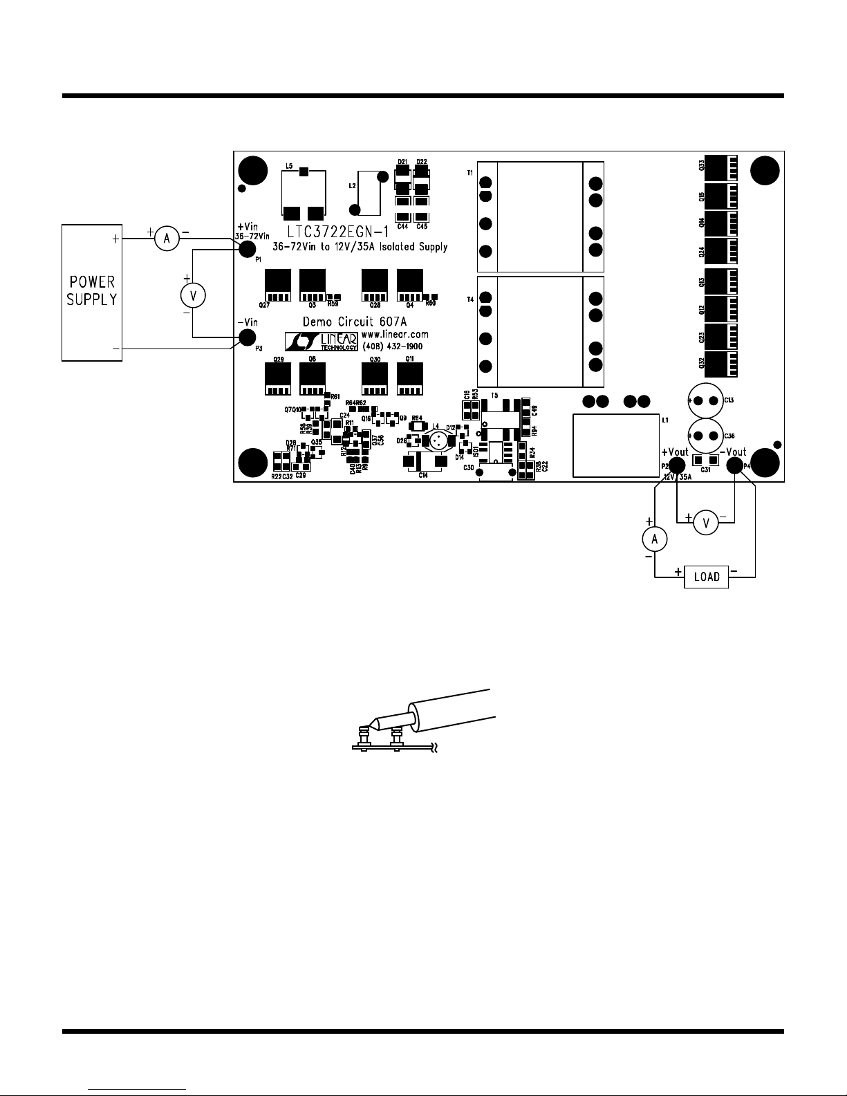
NOTE. When measuring the input or output voltage ripple,
care must be taken to avoid a long ground lead on the
oscilloscope probe. Measure the output (or input) voltage
ripple by touching the probe tip and probe ground directly
across the +Vout and –Vout (or +Vin and –Vin) terminals
or input/output capacitors. See Figure 2 for proper scope
probe technique.
1. Set an input power supply that is capable of 36V to 72V
to a voltage of 36V. Then turn off the supply.
2. With power off, connect the supply to the input terminals
+Vin and –Vin.
a. Input voltages lower than 36V can keep the converter
from turning on due to the undervoltage lockout
feature of the LTC3722.
b. If efficiency measurements are desired, an ammeter
capable of measuring 15Adc or a resistor shunt can
be put in series with the input supply in order to
measure the DC607A’s input current.
c. A voltmeter with a capability of measuring at least
can be placed across the input terminals in order
72V
to get an accurate input voltage measurement.
3. Turn on the power at the input.
NOTE. Make sure that the input voltage never exceeds
72V.
4. Check for the proper output voltage of 12V ±1%. Turn
off the power at the input.
5. Once the proper output voltage is established, connect
a variable load capable of sinking 35A at 12V to the
output terminals +Vout and –Vout. Set the current
for 0A.
a. If efficiency measurements are desired, an ammeter
or a resistor shunt that is capable of handling 35Adc
can be put in series with the output load in order to
measure the DC607A’s output current.
b. A voltmeter with a capability of measuring at least 12V
can be placed across the output terminals in order
to get an accurate output voltage measurement.
6. Turn on the power at the input.
NOTE. If there is no output, temporarily disconnect the
load to make sure that the load is not set too high.
7. Once the proper output voltage is again established,
adjust the load within the operating range and observe
the output voltage regulation, ripple voltage, efficiency
other desired parameters.
and
2
dc607afa
Page 3
Quick start proceDure
GND
DEMO MANUAL DC607A
Figure 1. Proper Measurement Equipment Setup
VIN
Figure 2. Measuring Input or Output Ripple
dc607afa
3
Page 4
DEMO MANUAL DC607A
Quick start proceDure
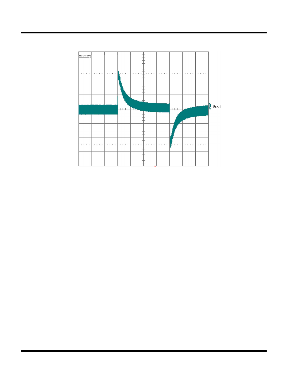
Figure 3. Transient Response, 0A to 35A, 48VIN (200mV and 0.5ms/Div)
4
dc607afa
Page 5

Quick start proceDure
DEMO MANUAL DC607A
Figure 4. Thermal Map, 48V
, 12V at 35A
IN
, 200LFM, Frontside
OUT
Figure 5. Thermal Map, 48VIN, 12V at 35A
, 200LFM, Backside
OUT
dc607afa
5
Page 6

DEMO MANUAL DC607A
Quick start proceDure
Figure 6. Thermal Map, 48V
, 12V at 35A
IN
, 400LFM, Frontside
OUT
Figure 7. Thermal Map, 48VIN, 12V at 35A
6
, 400LFM, Backside
OUT
dc607afa
Page 7

DEMO MANUAL DC607A
parts list
ITEM QTY REFERENCE PART DESCRIPTION MANUFACTURER/PART NUMBER
Required Circuit Components
1 6 C1, C2, C3, C4, C5, C46 CAP, X7R, 0.82µF, 100V, 10%, 1812 VISHAY, VJ1812Y824KXBAT
2 2 C24, C31 CAP, X7R, 1µF, 25V, 10%, 1206 AVX, 12063C105KAT2A
3 1 C7 CAP, NPO, 470pF, 200V, 10%, 1206 AVX, 12062A471K AT2A
4 1 C16 CAP, X7R, 0.1µF, 25V, 10%, 0805 AVX, 08053C104K AT2A
5 2 C13, C36 CAP, OSCON, 180µF, 16V, 20%, PANASONIC, 16SEP180M+TSS
6 1 C14 CAP, TANT, 68µF, 20V, 20%, 7343 AVX, TPSE686M020R0150
7 1 C21 CAP, X7R, 0.047µF, 25V, 10%, 0805 AVX, 08053C473K AT2A
8 1 C23 CAP, X7R, 0.022µF, 25V, 10%, 0805 AVX, 08053C223K AT2A
9 1 C26 CAP, X7R, 0.47µF, 25V, 10%, 1206 AVX, 12063C474K AT2A
10 1 C27 CAP, NPO, 330pF, 25V, 10%, 0805 AVX, 08053A331K AT2A
11 1 C28 CAP, NPO, 180pF, 25V, 10%, 0805 AVX, 08053A181K AT2A
12 2 C32, C49 CAP, NPO, 220pF, 25V, 5%, 0805 AVX, 08053A221J AT2A
13 1 C29 CAP, X7R, 0.068µF, 25V, 10%, 0805 AVX, 08053C683K AT2A
14 1 C30 CAP, CER, 2.2nF, 250V, +20,-55% MURATA, DE2E3KH222MB3BM02F
15 2 C34, C35 CAP, X7R, 0.22µF, 25V, 10% 0805 AVX, 08053C224K AT2A
16 1 C40 CAP, X7R, 2.2nF, 25V, 10%, 0603 AVX, 06033C222K AT2A
17 1 C41 CAP, NPO, 220pF, 25V, 5%, 0603 AVX, 06033A221J AT2A
18 2 C42, C43 CAP, NPO, 22pF, 25V, 10%, 0603 AVX, 06033A220
19
20 2 C47, C48 CAP, X5R, 1µF, 25V, 10% 0603 AVX, 06033D105K AT2A
21 1 C50 CAP, NPO 330pF, 25V, 10% 0603 AVX, 06033A331K AT2A
22 2 C58, C59 CAP, X7R 0.1µF, 16V, 10%, 0603 AVX, 0603YC104K AT2A
23 3 D21, D22, D25 SUPER-FAST RECTIFIER, MURS120 DIODES INC, MURS120-13-F
24 4 D12, D14, D23, D24 DIODE, FAST SWITCHING DIODE, SOT23 DIODES INC, BAS21-7-F
25 1 D16 DIODE, 10V, SOT23, DIODES INC, MMBZ5240B-7-F
26 1 D20 DIODE, 5.1V, SOT23 DIODES INC, MMBZ5231B-7-F
27 1 D26 DIODE, 3.3V, SOT23 DIODES INC, MMBZ5226B-7-F
28 1 D28 DIODE, SCHOTTKY, SOT23 DIODES INC, BAT54-7-F
29 1 ISO1 IC, OPTOISOLATORS, SO8 FAIRCHILD SEMI, MOC207M
30 1 L1 INDUCTOR, 0.85µH, PULSE, PA1294.910NL
31 1 L2 INDUCTOR, 150nH, PULSE, PA0651NL
32 1 L4 INDUCTOR, 1mH, DO1608C COILCRAFT, DO1608C-105MLB
33 1 L5 INDUCTOR, 1.3µH, CDEP105 SUMIDA, CDEP105-1R3MC-50
34 4 Q7, Q9, Q25, Q26 XSTR, NPN, SOT23 DIODE INC, FMMT619TA
35 16 Q3, Q4, Q8, Q11 TO Q15, Q23,
36 4 Q10, Q16 TO Q18 XSTR, PNP, SOT23 DIODE INC., FMMT718TA
37
38
39 5 R1, R4, R6, R8, R10 RES, 240, 1/4W, 5%, 1206 YAGEO, RC1206JR-07240RL
2 C44, C45 CAP, X7R, 0.47µF, 100V, 10% 1210 TDK CGA6M2X7R2A474K200AA
N-MOSFET, 80V, PowerPak-SO-8 INFINEON, BSC072N08NS5ATMA1
Q24, Q27 TO Q30, Q32, Q33
2 Q34, Q35 XSTR, NPN, SOT23 DIODE INC., MMBT3904-7-F
2 R2, R5 RES, 3.9k, 1/4W, 5%, 1206 VISHAY, CRCW12063K90JNEA
KAT2A
dc607afa
7
Page 8

DEMO MANUAL DC607A
parts list
ITEM QTY REFERENCE PART DESCRIPTION MANUFACTURER/PART NUMBER
40 2 R3, R91 RES, 1k, 1/16W, 5%, 0603 VISHAY, CRCW06031K00JNEA
41 1 R18 RES, 182k, 1/8W, 1%, 0805 VISHAY, CRCW0805182KFKEA
42 1 R22 RES, 30.1k, 1/8W, 1%, 0805 VISHAY, CRCW080530K1FKEA
43 1 R30 RES, 20k, 1/8W, 5%, 0805 VISHAY, CRCW080520K0JNEA
44 2 R32, R33 RES, 4.99k, 1/16W, 1%, 0603 VISHAY, CRCW06034K99FKEA
45 1 R37 RES, 470, 1/8W, 5%, 1206 VISHAY, CRCW1206470RJNEA
46 1 R38 RES, 330, 1/8W, 5%, 0805 VISHAY, CRCW0805330RJNEA
47 1 R39 RES, 150, 1/16W, 5%, 0805 VISHAY, CRCW0805150RJNEA
48 1 R40 RES, 2.7k, 1/16W, 5%, 0805 VISHAY, CRCW08052K70JNEA
49 1 R41 RES, 10k, 1/8W, 5%, 0805 VISHAY, CRCW080510K0JNEA
50 1 R42 RES, 9.53k, 1/8W, 1%, 0805 VISHAY, CRCW08059K53FKEA
51 1 R43 RES, 750, 1/8W, 5%, 0603 VISHAY, CRCW0603750RJNEA
52 1 R44 RES, 5.1k, 1/16W, 5%, 0603 VISHAY, CRCW06035K10JNEA
53 1 R46 RES, 2.49k, 1/8W, 1%, 0805 VISHAY, CRCW08052K49FKEA
54 1 R47 RES, 33k, 1/16W, 5%, 0603 VISHAY, CRCW060333K0JNEA
55 2 R48, R49 RES, 0.020, 2W,1%, 2512 STACKPOLE ELE. CSRN2512FK20L0
56 1 R53 RES, 22, 1/8W, 5%, 0805 VISHAY, CRCW080522R0JNEA
57 1 R58 RES, 10k, 1/16W, 5%, 0603 VISHAY, CRCW060310K0JNEA
58 2 R54, R55 RES, 80.6k, 1/16W, 1%, 0603 VISHAY, CRCW060380K6FKEA
59 1 R56 RES, 20k, 1/16W, 1%, 0603 VISHAY, CRCW060320K0FKEA
60 1 R71 RES, 8.25k, 1/16W, 1%, 0603 VISHAY, CRCW06038K25FKEA
61 4 R72 TO R75 RES, 100, 1W, 5%, 2512 VISHAY, CRCW2512100RJNEA
62 1 R84 RES, 100, 1/4W, 5%, 1206 VISHAY, CRCW1206100RJNEG
63 2 R85, R88 RES, 4.87k, 1/4W, 1%, 1206 VISHAY
64 2 R86, R89 RES, 9.09k, 1/16W, 1%, 0603 VISHA
65 2 R87, R90 RES, 3.16k, 1/16W, 1%, 0603 VISHAY, CRCW06033K16FKEA
66 1 R92 RES, 39.2k, 1/16W, 1%, 0603 VISHAY, CRCW060339K2FKEA
67 2 R65, R66 RES, 18.2k 1/16W, 1%, 0603 VISHAY, CRCW060318K2FKEA
68 1 R15 RES, 1M, 1/16W, 5%, 0603 VISHAY, CRCW06031M00JNEA
69 1 R93 RES, 100Ω 1/16W, 5%, 0603 VISHAY, CRCW0603100RJNEA
70 1 R94 RES, 100Ω 1/16W, 1%, 0805 VISHAY, CRCW0805100RFKEA
71 1 R95 RES, 200k, 1/16W, 5%, 0603 VISHAY, CRCW0603200KJNEA
72 2 T1, T4 TRANSFORMER PULSE, PA0526NL
73 1 T5 TRANSFORMER PULSE, PA0297NL
74 1 U1 IC, LTC3901EGN SSOP-16 LINEAR, LTC3901EGN#PBF
75 1 U2 IC, LTC3722EGN-1, SSOP-24GN LINEAR, LTC3722EGN-1#PBF
76 1 U3 IC, LT1431CS8, SO8 LINEAR, LT1431CS8#PBF
77 2 U5, U6 IC, LTC4440EMS8E,MSOP-8/Exposed LINEAR, LTC4440EMS8E#PBF
, CRCW12064K87FKEA
Y, CRCW06039K09FKEA
8
dc607afa
Page 9

DEMO MANUAL DC607A
parts list
ITEM QTY REFERENCE PART DESCRIPTION MANUFACTURER/PART NUMBER
Additional Demo Board Circuit Components
1 0 C19, C20, C22, C53, C56, C57 CAP, OPT, 0805 OPT
2 0 Q37 (OPT) XSTR, PNP, SOT23 OPT
3 0 R7 (OPT) RES, OPT, 1206 OPT
4 0 R9, R11, R12, R14, R31, R61,
R62
5 15 R13, R57, R59, R60, R63, R64,
R76 TO R83, R98
6 0 R23 TO R28, R34 (OPT) RES, OPT, 0805 OPT
7 1 R45 RES, 0 JUMPER, 0805 VISHAY, CRCW08050000Z0EA
8 2 R50, R51 RES, 33, 1/8W, 5%, 0805 VISHAY, CRCW080533R0JNEA
Hardware: For Demo Board Only
1 4 P1, P2, P3, P4 MICRO PINS, 0.08 PIN-SWAGE MOUNT KEYSTONE, 1455-2
2 4 STANDOFF STANDOFF, NYLON 0.50" TALL.HOLE 0.125 WURTH ELEKTRONIK, 702935000
3 1 PRINTED CIRCUIT BOARD DEMO CIRCUIT #607A
RES, OPT, 0603 OPT
RES, 0 JUMPER, 0603 VISHAY, CRCW06030000Z0EA
dc607afa
9
Page 10

DEMO MANUAL DC607A
schematic Diagram
VLOW
+VOUT
100V
C44
2x100,1W=50
R72,R73
VIN
L5
1.3uH
C7
470pF
5x240,0.25W=48
R1,R4,R6,R8,R10
C1
2x3.9K,0.25W=2k
R2,R5
VLOW
5:5(105uH):1:1
T1
4 11
D21
0.47uF
D22
C45
100V
0.47uF
D24
3
12V
D23
3
12V
200V
VHIGH
0.82uF
100V
-VOUT
D25
8
10
2
1W=50
2x100,
R74,R75
6
7
TG
BOOST
VCC
IN
1
C
08NS5
2xBSC072N
Q3,Q27
6
7
TG
BOOST
VCC
IN
1
A
4x0.82uF
100V
C3,C4,C5,C46
0.82uF
100V
C2
+VOUT
L1
VHIGH
11
7
4
2xBSC072N08NS5
Q4,Q28
C35
0.22uF
U6
TS
8
GND
2
GND
4
L2
0.1uF
C58
C34
0.22uF
U5
TS
8
GND
2
GND
4
0.1uF
C59
+Vout
12V/35A
2x180uF
C13,C36
+
0.85uH
Q14,Q15,Q24,Q33
4xBSC072N08NS5
7108
2
Q11,Q30
12V
Q9
LTC4440-EMS8E
D
150nH
Q8,Q29
12V
Q7
LTC4440-EMS8E
B
-Vout
1.0uF
C31
-VOUT
16V
+VOUT
Q26
+VOUT
Q25
4xBSC072N08NS5
Q12,Q13,Q23,Q32
D12
5:5(105uH):1:1
T4
2xBSC072N08NS5
L4
R84
Q16
12V
ISNS
2xBSC072N08NS5
Q10
6
1.0mH
C14
R3
100
R89
R86
+
68uF
9.09K
9.09K
D26
20V
1K
D14
Q34
R91
1K
D16
10V
MMBT3904
1
PVCC
SYNC
U1
R94
C43
C42
C16
R33
R32
5
8
100
TIMER
PGND2
GND2
PGND
GND
0.1uF
22pF
4.99k
22pF
4.99k
R53
C48
C47
7
4
8
13
10
22
D
C
B
A
1uF
1uF
C50
C49
5VREF
ISNS
12V
330pF
220pF
R95
R30
LINEAR TECHNOLOGY CORPORATION
-VOUT
R41
10K
+VOUT
R40
2.7K
R37
470 1/4W
0.047uF
C21
330
R38
1
750
R43
200K
3
OUTE
CS
16
OUTF
15
OUTD
17
OUTC
19
OUTB
20
OUTA
21
PDLY
9
U2
LTC3722EGN-1
ADLY
11
SBUS
VIN
10
18
150
R39
20K
1/4W
CUSTOMER NOTICE
CONFIDENTIAL
THIS CIRCUIT IS DISTRIBUTED
TO CUSTOMERS ONLY FOR USE
WITH LTC PARTS.
LINEAR TECHNOLOGY HAS MADE A BEST EFFORT TO DESIGN A CIRCUIT
THAT MEETS CUSTOMER-SUPPLIED SPECIFICATIONS; HOWEVER, IT
REMAINS THE CUSTOMER'S RESPONSIBILITY TO VERIFY PROPER AND
RELIABLE OPERATION IN THE ACTUAL APPLICATION. COMPONENT
22nF
C23
R46
R42
9.53K
8
RTOP
COMP
V+
1
MOC207
REF
COLL
2
5
C30
RMID
GND-S
GND-F
2.2nF
4
2
3
ISO1
6
C40
COMP
4
R15
D28
SS
7
PGND
22
R71
8.25K
GND
23
FB
6
RLEB
5
12
SPRG
CT
SYNC
NC
DPRG
VREF
UVLO
1
8
2
13
24
14
R44
R56
5VREF
R58
5.1K
C41
20.0K
C26
SUBSTITUTION AND PRINTED CIRUIT BOARD LAYOUT MAY SIGNIFICANTLY
AFFECT CIRCUIT PERFORMANCE OR RELIABILITY. CONTACT LINEAR
TECHNOLOGY APPLICATIONS ENGINEERING FOR ASSISTANCE.
2.49K
-VOUT
U3
LT1431CS8
7
5
6
D20
5.1V
250V
2.2nF
330pF
C27
1M
MMBT3904
Q35
C29
68nF
R47
33K
Figure 8. Schematic without Optional Components
10K
C28
180pF
220pF
0.47uF
C24
1.0uF
220pF
C32
+VOUT
100
R93
39.2K
R92
VCC
16
MF2
R90
R88
R87
R85
3.16K
4.87K
3.16K
4.87K
1/4W
1/4W
15
14
12
11
3
2
5
6
MF
CSF-
CSF+
ME2
ME
CSE-
CSE+
T5
1(1.5mH):0.5
LTC3901EGN
9
4
1
Q18
Q17
1
3.3V
0.020
2W
R49
80.6K
R48
0.020
2W
R55
R54
C
R66
18.2K
80.6K
5VREF
R65
18.2K
B
VIN
R18
182K
R22
30.1K
+Vin
36-72Vin
-Vin
0.47uF, 100V TDK C3225X7R2A474K (1210)
0.82uF, 100V Vishay VJ1812Y824KXBAT (1812)
180uF, 16V Panasonic 16SEP180M+TSS
10
C14 AVX TPSE686M020R0150
C30 MuRata DE2E3KH222MB3B
D21,D22,D25 MURS120T3
D23,D24,D12,D14 BAS21
D26 3.3V MMBZ5226B
D28 BAT54
D16 10V MMBZ5240B
D20 5.1V MMBZ5231B
L1 PA1294.910
L2 Pulse PA0651
L4 Coilcraft DO1608C-105
L5 Sumida CDEP105-1R3MC-50
Q7,Q9,Q25,Q26 Diodes Inc FMMT619
Q10,Q16,Q17,Q18 Diodes Inc FMMT718
T1,T4 Pulse PA0526
T5 Pulse PA0297
dc607afa
Page 11

DEMO MANUAL DC607A
5
4
3
2
1
schematic Diagram
A
A
A
1
1
1
REV
REV
REV
OF
OF
P2
+Vout
12V/35A
+VOUT
3.9K
opt.
1/4W
1/4W
3.9K
1/4W
R5
R7
R2
C1
0.82uF
100V
-VOUT
VLOW +VOUT
C7
470pF
R6
R4
R1
1/4W
1/4W
240
240
240 1/4W
200V
R10
R8
240
1/4W
1/4W
VHIGH
240
VLOW
5:5(105uH):1:1
T1
1
4 11
6
D21
D22
100V
C44
0.47uF
R73
100 1W
U6
LTC4440-EMS8E
100V
C45
0.47uF
D24
BAS21
12V
R72
100 1W
Q27
Q3
D25
L1
0.85uH
7108
2
4 11
1W
R75
100
R74
1W
100
2 3
6 7 8
5
1
Q28
4
Q4
2 3
6 7 8
5
1
4
0
R60
A_LEG
7
6
C35
TS
TG
GND
BOOST
VCC
GND
3
IN
1
C
C58
2 3
6 7 8
0.1uF
5
1
4
2 3
6 7 8
5
1
4
0
R59
P_LEG
7
6
D23
TG
BAS21
BOOST
VCC
3
U5
LTC4440-EMS8E
VIN
L5
1.3uH
P1
+Vin
D D
12V
36-72Vin
IN
1
A
C59
C46
0.82uF
100V
C5
0.82uF
100V
C4
0.82uF
100V
C3
0.82uF
100V
C2
0.82uF
100V
Q33
Q24
Q15
MURS120
Q14
Q32
Q23
VHIGH
Q13
Q12
0.22uF
8
2
4
16V
C34
0.22uF
TS
8
GND
2
GND
4
16V
0.1uF
P3
+
+
L2
P_LEG
-Vin
C36
C13
5
678
150nH
C31
5
678
5
678
5
678
5
678
5
678
5
678
5
678
12V
180uF
180uF
2
MB
1.0uF
P4
-Vout
16V
16V
4
1
23
4
1
23
4
1
23
4
1
23
4
1
23
4
1
23
4
1
23
4
1
23
7108
Q30
6 7 8
5
4
6 7 8
5
4
Q11
12V
Q9
R62
MD
R64
Q29
6 7 8
5
4
6 7 8
5
Q8
4
Q7
R61
opt
0
R63
B
+VOUT
-VOUT
Q26
R89
R86
-VOUT
R51
9.09K
R50
9.09K
33
33
+VOUT
R90
R87
R85
R88
Q34
3.16K
4.87K
3.16K
4.87K
1/4W
1/4W
R91
32
MMBT3904
16
15
14
12
11
3
2
5
6
0
R83
0
R82
0
R81
0
R80
0
R79
0
R78
0
R77
0
R76
Q18
+VOUT
ME MF
Q25
Q17
MF
VLOW
ME
VHIGH
5:5(105uH):1:1
T4
1
6
D14
D12
L4
2 3
1.0mH
1
3.3V
100
2 3
1
D26
R84
MMBZ5226B
C14
20V
68uF
+
12V
Q16
opt
0
D
ISNS
1K
R3
2 3
1
2 3
1
R49
0.020
2W
R48
2W
0.020
Q10
OPT.
C20
PDLY5VREF 5VREF
P_LEG
R25
R28
OPT.
OPT.
OPT.
C19
ADLY
A_LEG
R27
R24
OPT.
OPT.
VIN
C C
R26
R23
OPT.
OPT.
1K
R54
R93
R92
U1
R55
SBUS
1
100
39.2K
80.6K
80.6K
1
Vcc
PVcc
MF2
MF
CSF-
CSF+
ME2
ME
CSE-
CSE+
SYNC
9
LTC3901EGN
4
T5
1
CB
R66
18.2K
R33
4.99K
R65
18.2K
R32
4.99K
R31
OPT.
R94
C16
R53
D16
C48
C47
TIMER
PGND2
GND2
PGND
GND
100
5
8
MMBZ5240B
10V
1uF
1uF
C50
7
13
10
4
8
C49
220pF
0.1uF
22
PDLY
R14
ADLY
B B
C43
C42
330pF
OPT.
22pF
22pF
-VOUT
+VOUT
R37
5VREF
ISNS
C DA
B
12V
VIN
SBUS
R95
16
15
17
19
20
21
9
11
R30
1/4W
470
opt.
C57
R38
330
ISO1
200K
10
R39
20K
R41
R42
R40
2.7K
C22
opt.
1
3478
MOC207
750
R43
3
CS
OUTE
OUTF
OUTD
OUTC
OUTB
OUTA
LTC3722EGN-1
U2
PDLY
ADLY
VIN18SBUS
150
R18
182k
10K
9.53K
2
3
Q35
UVLO
12
C23
8
RTOP4RMID
COMP
V+
1
C21
6
R98
MMBT3904
COMP
4
SS
7
PGND
22
GND
23
FB
6
RLEB
5
SPRG
13
CT
CT
24
SYNC
1
NC
8
DPRG
2
VREF
14
0.022uF
REF
COLL
0.047uF
2
5
0
R9
C40
2.2nF
R71
R44
R56
5VREF
R57
R22
C28
5.1K
20.0K
C32
30.1k
R46
U3
LT1431CS8
7
GND-S
5
GND-F
6
D20
R34
opt.
R45
opt.
C27
8.25K
R58
10K
180pF
C41
220pF
C26
0
C24
220pF
2.49K
5.1V
0
330pF
R47
0.47uF
1.0uF
1630 McCarthy Blvd.
Milpitas, CA 95035
Phone: (408)432-1900
Fax: (408)434-0507
1630 McCarthy Blvd.
Milpitas, CA 95035
Phone: (408)432-1900
Fax: (408)434-0507
1630 McCarthy Blvd.
Milpitas, CA 95035
Phone: (408)432-1900
Fax: (408)434-0507
TECHNOLOGY
TECHNOLOGY
TECHNOLOGY
DATE
DATE
DATE
APPROVALS
APPROVALS
APPROVALS
CONTRACT NO.
CONTRACT NO.
CONTRACT NO.
-VOUT
CUSTOMER NOTICE
CUSTOMER NOTICE
CUSTOMER NOTICE
LINEAR TECHNOLOGY HAS MADE A BEST EFFORT TO DESIGN A
CIRCUIT THAT MEETS CUSTOMER-SUPPLIED SPECIFICATIONS;
LINEAR TECHNOLOGY HAS MADE A BEST EFFORT TO DESIGN A
CIRCUIT THAT MEETS CUSTOMER-SUPPLIED SPECIFICATIONS;
LINEAR TECHNOLOGY HAS MADE A BEST EFFORT TO DESIGN A
CIRCUIT THAT MEETS CUSTOMER-SUPPLIED SPECIFICATIONS;
MMBZ5231B
C30
2.2nF
250V
C53
opt.
0
R13
D28
BAT54
R15
1M
C29
68nF
33K
R12
opt.
C56
opt.
5VREF
opt.
R11
Q37
CT
Note: UNLESS NOTED:
All caps 25V;
All resistors 0603 (1/16W) or 0805 (1/8W);
Q3, Q4, Q8, Q11-15,Q23,Q24,Q27-Q30,
Q32,Q33 Infineon BSC072N08NS5;
Q7, Q9,Q25,Q26 Diodes Inc FMMT619;
Q10, Q16-18 Diodes Inc FMMT718;
D12, D14, D23, D24 BAS21;
L2 Pulse PA0651;
L1 PA1294.910;
A A
OF
1
1
1
SHEET
DC607A
SHEET
DC607A
SHEET
DC607A
1
DWG NO
DWG NO
DWG NO
FILENAME:
FILENAME:
FILENAME:
CAGE CODE
CAGE CODE
CAGE CODE
LTC3722EGN-1, 36-72Vin to 12V/35A Isolated Supply
LTC3722EGN-1, 36-72Vin to 12V/35A Isolated Supply
LTC3722EGN-1, 36-72Vin to 12V/35A Isolated Supply
SIZE
SIZE
SIZE
SCALE:
SCALE:
SCALE:
TITLE
TITLE
TITLE
June Wu 9/13/02
June Wu 9/13/02
June Wu 9/13/02
Kurk Mathews 9/13/02
Kurk Mathews 9/13/02
Kurk Mathews 9/13/02
Tuesday, April 11, 2017
Tuesday, April 11, 2017
Tuesday, April 11, 2017
DRAWN
CHECKED
APPROVED
ENGINEER
DESIGNER
DRAWN
CHECKED
APPROVED
ENGINEER
DESIGNER
DRAWN
CHECKED
APPROVED
ENGINEER
DESIGNER
2
THIS CIRCUIT IS PROPRIETARY TO LINEAR TECHNOLOGY AND
SUPPLIED FOR USE WITH LINEAR TECHNOLOGY PARTS.
THIS CIRCUIT IS PROPRIETARY TO LINEAR TECHNOLOGY AND
SUPPLIED FOR USE WITH LINEAR TECHNOLOGY PARTS.
THIS CIRCUIT IS PROPRIETARY TO LINEAR TECHNOLOGY AND
SUPPLIED FOR USE WITH LINEAR TECHNOLOGY PARTS.
HOWEVER, IT REMAINS THE CUSTOMER'S RESPONSIBILITY TO
VERIFY PROPER AND RELIABLE OPERATION IN THE ACTUAL
APPLICATION. COMPONENT SUBSTITUTION AND PRINTED
CIRCUIT BOARD LAYOUT MAY SIGNIFICANTLY AFFECT CIRCUIT
PERFORMANCE OR RELIABILITY. CONTACT LINEAR
TECHNOLOGY APPLICATIONS ENGINEERING FOR ASSISTANCE.
3
Figure 9. Schematic with Optional Components
T5 Pulse PA0297;
T1,T4 Pulse PA0526;
D21,D22,D25 MURS120;
4
5
dc607afa
opt.
L5 Sumida CDEP105-1R3MC-50;
L4 Coilcraft DO1608C-105;
Information furnished by Linear Technology Corporation is believed to be accurate and reliable.
However, no responsibility is assumed for its use. Linear Technology Corporation makes no representation that the interconnection of its circuits as described herein will not infringe on existing patent rights.
11
Page 12

DEMO MANUAL DC607A
DEMONSTRATION BOARD IMPORTANT NOTICE
Linear Technology Corporation (LT C) provides the enclosed product(s) under the following AS IS conditions:
This demonstration board (DEMO BOARD) kit being sold or provided by Linear Technology is intended for use for ENGINEERING DEVELOPMENT
OR EVALUATION PURPOSES ONLY and is not provided by LT C for commercial use. As such, the DEMO BOARD herein may not be complete
in terms of required design-, marketing-, and/or manufacturing-related protective considerations, including but not limited to product safety
measures typically found in finished commercial goods. As a prototype, this product does not fall within the scope of the European Union
directive on electromagnetic compatibility and therefore may or may not meet the technical requirements of the directive, or other regulations.
If this evaluation kit does not meet the specifications recited in the DEMO BOARD manual the kit may be returned within 30 days from the date
of delivery for a full refund. THE FOREGOING WARRANTY IS THE EXCLUSIVE WARRANTY MADE BY THE SELLER TO BUYER AND IS IN LIEU
OF ALL OTHER WARRANTIES, EXPRESSED, IMPLIED, OR STATUTORY, INCLUDING ANY WARRANTY OF MERCHANTABILITY OR FITNESS
FOR ANY PARTICULAR PURPOSE. EXCEPT TO THE EXTENT OF THIS INDEMNITY, NEITHER PARTY SHALL BE LIABLE TO THE OTHER FOR
ANY INDIRECT, SPECIAL, INCIDENTAL, OR CONSEQUENTIAL DAMAGES.
The user assumes all responsibility and liability for proper and safe handling of the goods. Further, the user releases LT C from all claims
arising from the handling or use of the goods. Due to the open construction of the product, it is the user’s responsibility to take any and all
appropriate precautions with regard to electrostatic discharge. Also be aware that the products herein may not be regulatory compliant or
agency certified (FCC, UL, CE, etc.).
No License is granted under any patent right or other intellectual property whatsoever. LTC assumes no liability for applications assistance,
customer product design, software performance, or infringement of patents or any other intellectual property rights of any kind.
LT C currently services a variety of customers for products around the world, and therefore this transaction is not exclusive.
Please read the DEMO BOARD manual prior to handling the product. Persons handling this product must have electronics training and
observe good laboratory practice standards. Common sense is encouraged.
This notice contains important safety information about temperatures and voltages. For further safety concerns, please contact a LTC application engineer.
Mailing Address:
Linear Technology
1630 McCarthy Blvd.
Milpitas, CA 95035
Copyright © 2004, Linear Technology Corporation
12
dc607afa
LT 0417 REV A • PRINTED IN USA
LINEAR TECHNOLOGY CORPORATION 2015
 Loading...